Modulators and Semiconductors ERIC MITCHELL AcoustoOptic Modulators Based
Modulators and Semiconductors ERIC MITCHELL
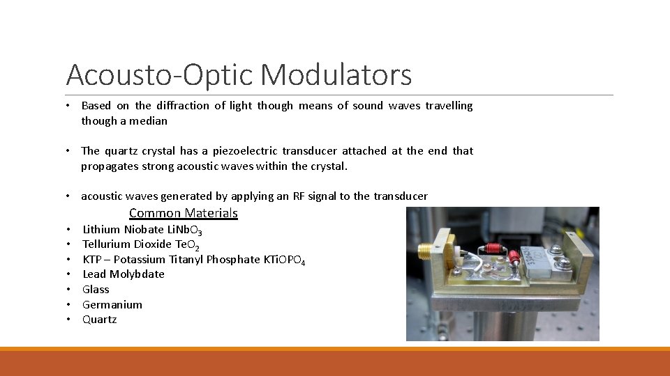
Acousto-Optic Modulators • Based on the diffraction of light though means of sound waves travelling though a median • The quartz crystal has a piezoelectric transducer attached at the end that propagates strong acoustic waves within the crystal. • acoustic waves generated by applying an RF signal to the transducer Common Materials • • Lithium Niobate Li. Nb. O 3 Tellurium Dioxide Te. O 2 KTP – Potassium Titanyl Phosphate KTi. OPO 4 Lead Molybdate Glass Germanium Quartz
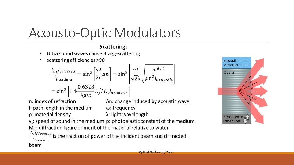
Acousto-Optic Modulators
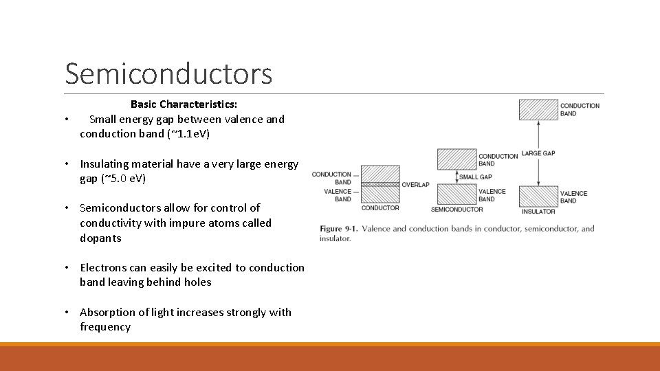
Semiconductors Basic Characteristics: • Small energy gap between valence and conduction band (~1. 1 e. V) • Insulating material have a very large energy gap (~5. 0 e. V) • Semiconductors allow for control of conductivity with impure atoms called dopants • Electrons can easily be excited to conduction band leaving behind holes • Absorption of light increases strongly with frequency
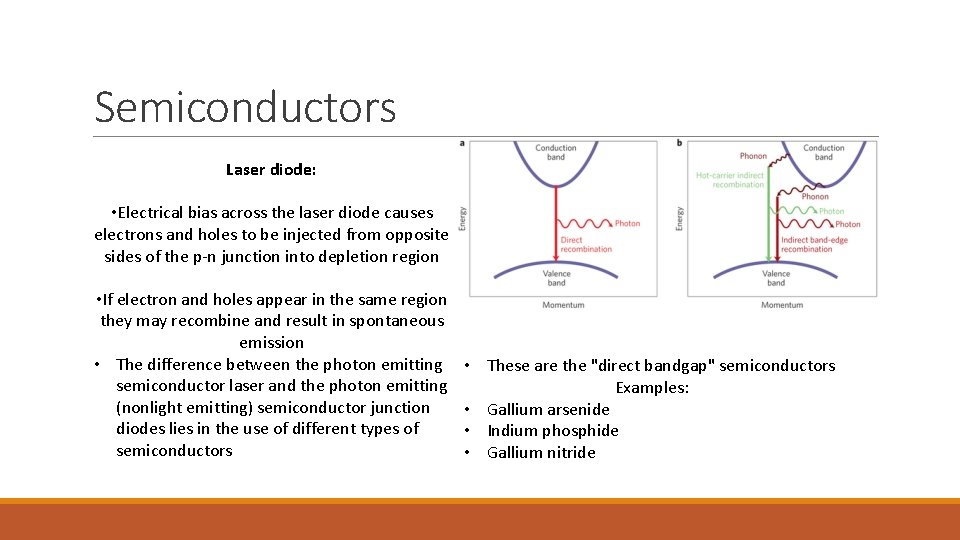
Semiconductors Laser diode: • Electrical bias across the laser diode causes electrons and holes to be injected from opposite sides of the p-n junction into depletion region • If electron and holes appear in the same region they may recombine and result in spontaneous emission • The difference between the photon emitting semiconductor laser and the photon emitting (nonlight emitting) semiconductor junction diodes lies in the use of different types of semiconductors • These are the "direct bandgap" semiconductors Examples: • Gallium arsenide • Indium phosphide • Gallium nitride
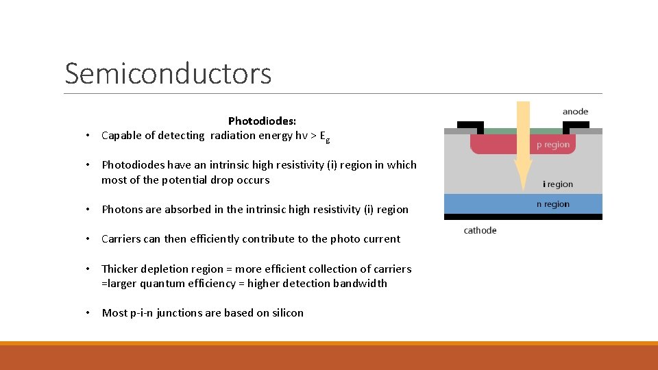
Semiconductors Photodiodes: • Capable of detecting radiation energy hv > Eg • Photodiodes have an intrinsic high resistivity (i) region in which most of the potential drop occurs • Photons are absorbed in the intrinsic high resistivity (i) region • Carriers can then efficiently contribute to the photo current • Thicker depletion region = more efficient collection of carriers =larger quantum efficiency = higher detection bandwidth • Most p-i-n junctions are based on silicon
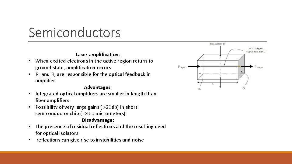
Semiconductors • • • Laser amplification: When excited electrons in the active region return to ground state, amplification occurs R 1 and R 2 are responsible for the optical feedback in amplifier Advantages: Integrated optical amplifiers are smaller in length than fiber amplifiers Possibility of very large gains ( >20 db) in short semiconductor chip ( <400 micrometers) Disadvantage: The presence of residual reflections and the resulting need for optical isolators reflections can give rise to instabilities and noise
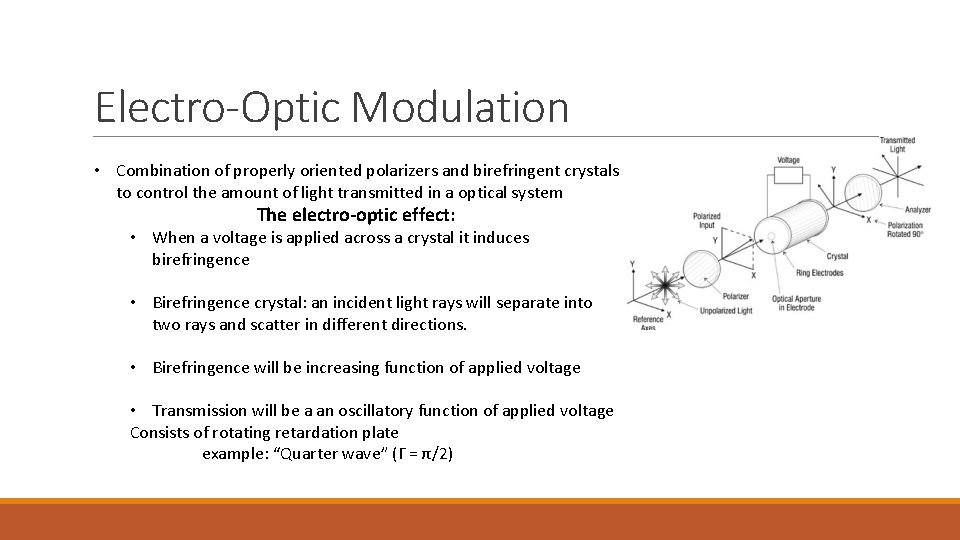
Electro-Optic Modulation • Combination of properly oriented polarizers and birefringent crystals to control the amount of light transmitted in a optical system The electro-optic effect: • When a voltage is applied across a crystal it induces birefringence • Birefringence crystal: an incident light rays will separate into two rays and scatter in different directions. • Birefringence will be increasing function of applied voltage • Transmission will be a an oscillatory function of applied voltage Consists of rotating retardation plate example: “Quarter wave” (Γ = π/2)
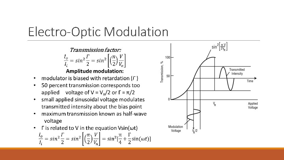
Electro-Optic Modulation
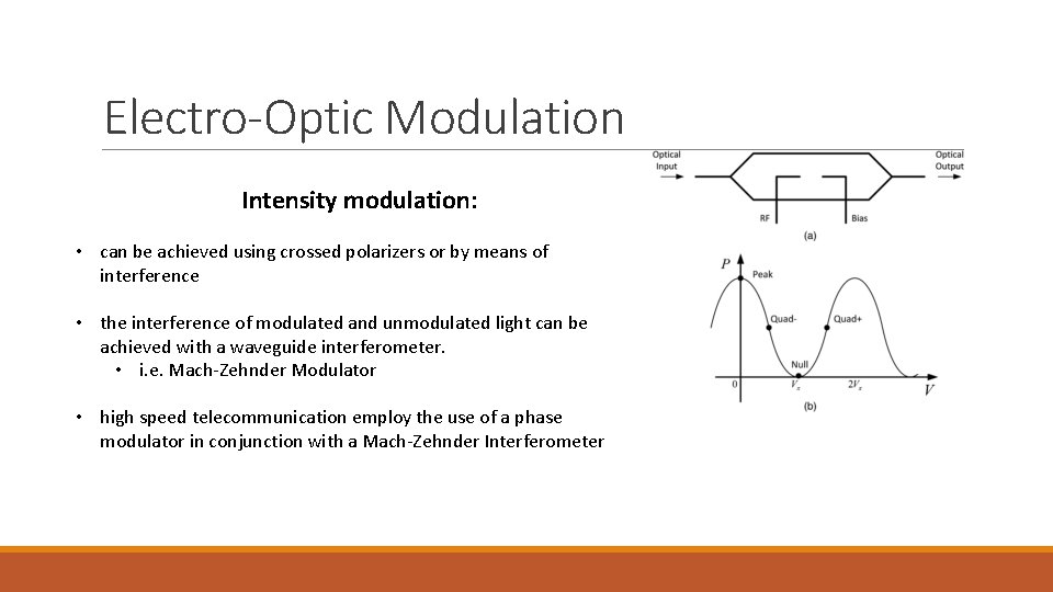
Electro-Optic Modulation Intensity modulation: • can be achieved using crossed polarizers or by means of interference • the interference of modulated and unmodulated light can be achieved with a waveguide interferometer. • i. e. Mach-Zehnder Modulator • high speed telecommunication employ the use of a phase modulator in conjunction with a Mach-Zehnder Interferometer
References Yariv, Optical electronics Oshea, Rodes An Introduction to Laser and their Applications Silfvast, T. William Laser Fundamentals Simcick, John ELECTRO-OPTIC AND ACOUSTO-OPTIC DEVICES What When how, Optical Time-Division Multiplexed Communication Networks Part 5
- Slides: 11