Modular Design Techniques for the Field Programmable Port

Modular Design Techniques for the Field Programmable Port Extender John Lockwood and David Taylor Washington University http: //www. arl. wustl. edu/arl/projects/fpx/ Field Programmable Port Extender (FPX) 1

FPX System-On-Chip Components • Infrastructure: – All components on chip to implement system functions • • SRAM Interface SDRAM Interface Control cell processor Reconfiguration control • Modules: – Entities that perform specific network function • Packet classification • Data compression • Data encryption, etc. – Standard module interface • Ensures module interoperability • Reduces design redundancy • Shortens module design cycle Field Programmable Port Extender (FPX) 2
![Network Module Hardware Interface D_MOD_IN[31: 0] SOC_MOD_IN TCA_MOD_OUT fpx_module. vhd SRAM_GR SRAM_D_IN[35: 0] Grant Network Module Hardware Interface D_MOD_IN[31: 0] SOC_MOD_IN TCA_MOD_OUT fpx_module. vhd SRAM_GR SRAM_D_IN[35: 0] Grant](http://slidetodoc.com/presentation_image_h2/2dab72473466df8b4c0c1b12ad1923f8/image-3.jpg)
Network Module Hardware Interface D_MOD_IN[31: 0] SOC_MOD_IN TCA_MOD_OUT fpx_module. vhd SRAM_GR SRAM_D_IN[35: 0] Grant 2 Grant 1 SDRAM_DATA[63: 0] CLK RESET_L ENABLE_L Data Interface FPX Network Module SRAM Interface SDRAM Interface Module Interface Field Programmable Port Extender (FPX) D_MOD_OUT[31: 0] SOC_MOD_OUT TCA_MOD_IN SRAM_REQ SRAM_D_OUT[35: 0] SRAM_ADDR[17: 0] SRAM_WR_RD Request Info. Bus[22: 0] READY_L 3

RAD Module Interface • Cell I/O and Flow Control – 32 -bit wide UTOPIA-style interface w/ unique timing • Off-chip Memory Access – Arbitrated access to SRAM and SDRAM via standard interface • Control (clock, reset, and reconfiguration control) Field Programmable Port Extender (FPX) 4

Control Interface • 100 MHz global clock (CLK) – All I/O signals should be synchronous to CLK • Synchronous reset (RESET_L) – Asserted low for 1 clock cycle • Reconfiguration handshake (ENABLE_L, READY_L) – Enable asserted low at reset – Module must pull READY_L high after reset, prior to accepting cells in order to prevent reconfiguration during operation – Enable asserted high prior to reconfiguration – Module stops accepting cells, flushes internal pipelines, and asserts READY_L for at least one clock cycle Field Programmable Port Extender (FPX) 5

Cell Input Interface • Start of Cell (SOC_MOD_IN) – Signals the first word of the ATM cell • 32 -bit wide data path (D_MOD_IN) – ATM cells transferred as (14) 32 -bit words – First word arrives with SOC_MOD_IN – Remaining 13 words arrive on subsequent clock cycles • Transmit Cell Available (TCA_MOD_IN) – Signals module’s ability to accept a cell – Must be valid 6 clock cycles prior to the last cycle of the current cell transfer Field Programmable Port Extender (FPX) 6

Cell Output Interface • Start of Cell (SOC_OUT_MOD) – Signals the first word of the ATM cell • 32 -bit wide data path (D_OUT_MOD) – ATM cells transferred as (14) 32 -bit words – First word sent with SOC_MOD_IN – Remaining 13 words sent on subsequent clock cycles • Transmit Cell Available (TCA_OUT_MOD) – Signals output’s ability to accept a cell – Modules must sample TCA_OUT_MOD no sooner than 3 clock cycles prior to asserting SOC_OUT_MOD Field Programmable Port Extender (FPX) 7

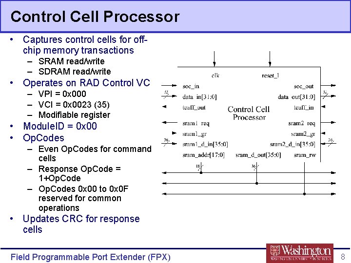
Control Cell Processor • Captures control cells for offchip memory transactions – SRAM read/write – SDRAM read/write • Operates on RAD Control VC – VPI = 0 x 000 – VCI = 0 x 0023 (35) – Modifiable register • Module. ID = 0 x 00 • Op. Codes – Even Op. Codes for command cells – Response Op. Code = 1+Op. Code – Op. Codes 0 x 00 to 0 x 0 F reserved for common operations • Updates CRC for response cells Field Programmable Port Extender (FPX) 8

FPX SRAM – Provide low latency for fast table-lookups – Zero Bus Turnaround (ZBT) allows back-to-back read / write operations every 10 ns – Dual, Independent Memories – 36 -bit wide bus Field Programmable Port Extender (FPX) 9

SRAM Interface Module • Interface to off-chip ZBT SRAM • Abstracts modules from device specific timing • Independent interface for each module • Arbitrates requests and issues grant to winning module • Modules retain access by holding request high after receiving grant – Modules responsible for preventing starvation Field Programmable Port Extender (FPX) 10

SRAM Interface Timing • All I/O signals must be flopped at module boundary to ensure timing constraints are met • Timing diagrams take reference point from inside module and assume boundary flops Field Programmable Port Extender (FPX) 11

FPX SDRAM – – – Dual, independent SDRAM memories 64 -bit wide, 100 MHz 64 MByte / Module : 128 Mbyte total [expandable] Burst-based transactions [1 -8 word transfers] Latency of 14 cycles to Read/Write 8 -word burst Field Programmable Port Extender (FPX) 12

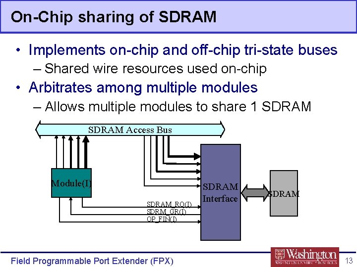
On-Chip sharing of SDRAM • Implements on-chip and off-chip tri-state buses – Shared wire resources used on-chip • Arbitrates among multiple modules – Allows multiple modules to share 1 SDRAM Access Bus Module(I) SDRAM_RQ(I) SDRM_GR(I) OP_FIN(I) Field Programmable Port Extender (FPX) SDRAM Interface SDRAM 13

Control Cell Processor • Captures control cells for offchip memory transactions – SRAM read/write – SDRAM read/write • Operates on RAD Control VC – VPI = 0 x 000 – VCI = 0 x 0023 (35) – Modifiable register • Module. ID = 0 x 00 • Op. Codes – Even Op. Codes for command cells – Response Op. Code = 1+Op. Code – Op. Codes 0 x 00 to 0 x 0 F reserved for common operations • Updates CRC for response cells Field Programmable Port Extender (FPX) 14

Design Issues & Recommendations • Conform to the Module Interface Specification – Make your design as easy to integrate as possible • Use provided infrastructure – Enables resources on the FPGA to be shared • Use Synchronous Design Techniques – Flop all module I/O signals – Use synchronous reset • Simulate Design – Verify that the device • Synthesize Design – Over-constrain timing delays – Optimize along the critical path of the circuit • Share experience and wisdom with other developers Field Programmable Port Extender (FPX) 15

Evolvable Internet Hardware Platform – Allow System Integration • Compile-time integration • Run-time configuration – Provide Modular Design • Use Standard Interfaces – Utopia Network interfaces for Gigabit links – Memory controllers for SRAM and SDRAM • Reuse Hardware Libraries – Internet Protocol Wrapper Library – ATM / AAL 5 / IP / UDP – Enable Rapid Prototype Field Programmable Port Extender (FPX) 16
- Slides: 16