Modified FEMB for the CRYO ASIC Kurtis Nishimura
Modified FEMB for the CRYO ASIC Kurtis Nishimura University of Hawaii In close collaboration with SLAC Cold Electronics Workshop July 17, 2018
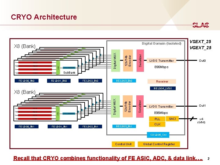
CRYO Architecture Digital Domain (Isolated) Serializer 12 b/14 b Encoder Digital MUX X 8 (Bank) LVDS Transmitter VSEXT_25 VGEXT_25 Out 0 896 Mbps Sub. Bank FE LDO 0_Bk 0 FE LDO 1_Bk 0 FE LDO 2_Bk 0 BE LDO 3_Bk 0 Receiver BE LDO 4_LVDS Serializer 12 b/14 b Encoder Digital MUX X 8 (Bank) LVDS Transmitter 896 Mbps PLL FE LDO 0_Bk 1 FE LDO 1_Bk 1 FE LDO 2_Bk 1 BE LDO 3_Bk 1 Out 1 SACI CLK x 4 (LVDS) CU LDO 5_Ctrl Control Unit Global Control Register Recall that CRYO combines functionality of FE ASIC, ADC, & data link…. 2
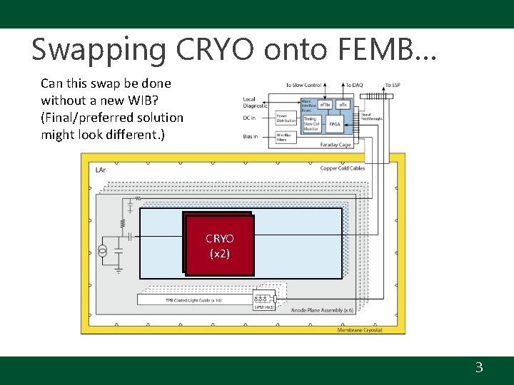
Swapping CRYO onto FEMB… Can this swap be done without a new WIB? (Final/preferred solution might look different. ) CRYO (x 2) 3
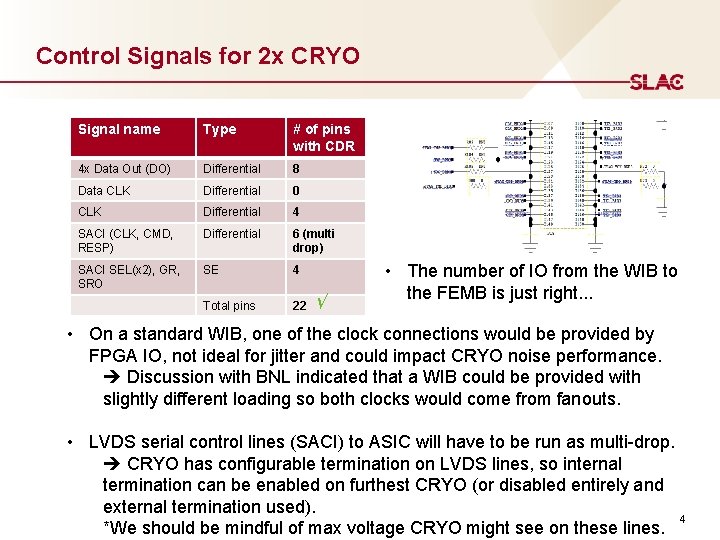
Control Signals for 2 x CRYO Signal name Type # of pins with CDR 4 x Data Out (DO) Differential 8 Data CLK Differential 0 CLK Differential 4 SACI (CLK, CMD, RESP) Differential 6 (multi drop) SACI SEL(x 2), GR, SRO SE 4 Total pins 22 √ • The number of IO from the WIB to the FEMB is just right. . . • On a standard WIB, one of the clock connections would be provided by FPGA IO, not ideal for jitter and could impact CRYO noise performance. Discussion with BNL indicated that a WIB could be provided with slightly different loading so both clocks would come from fanouts. • LVDS serial control lines (SACI) to ASIC will have to be run as multi-drop. CRYO has configurable termination on LVDS lines, so internal termination can be enabled on furthest CRYO (or disabled entirely and external termination used). 4 *We should be mindful of max voltage CRYO might see on these lines.
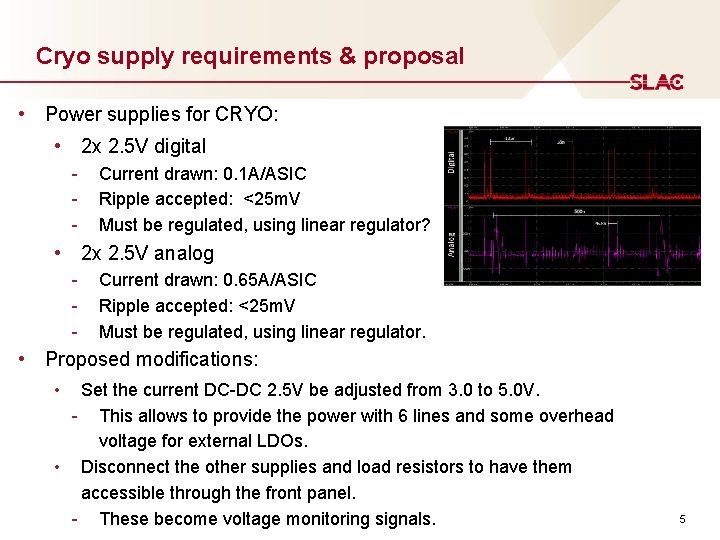
Cryo supply requirements & proposal • Power supplies for CRYO: • 2 x 2. 5 V digital - Current drawn: 0. 1 A/ASIC Ripple accepted: <25 m. V Must be regulated, using linear regulator? • 2 x 2. 5 V analog - Current drawn: 0. 65 A/ASIC Ripple accepted: <25 m. V Must be regulated, using linear regulator. • Proposed modifications: • Set the current DC-DC 2. 5 V be adjusted from 3. 0 to 5. 0 V. - This allows to provide the power with 6 lines and some overhead voltage for external LDOs. • Disconnect the other supplies and load resistors to have them accessible through the front panel. - These become voltage monitoring signals. 5
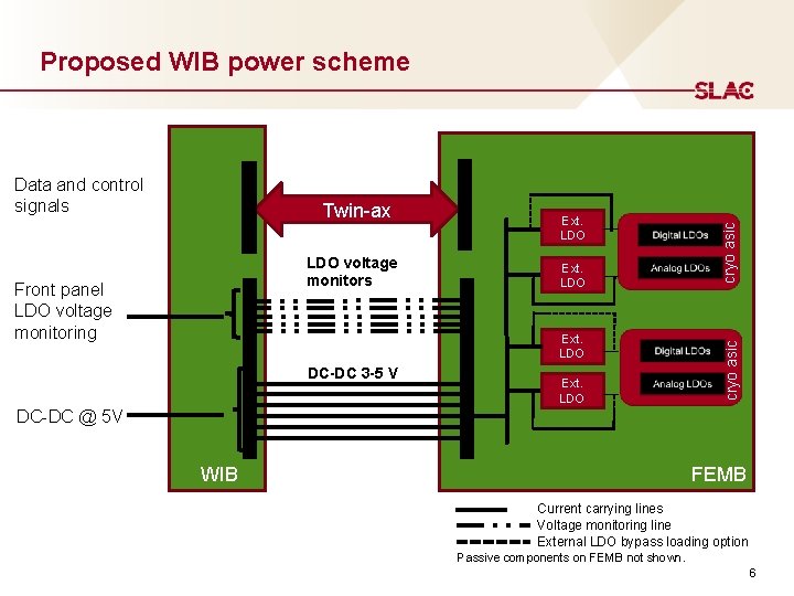
Twin-ax LDO voltage monitors Front panel LDO voltage monitoring Ext. LDO DC-DC 3 -5 V Ext. LDO cryo asic Data and control signals cryo asic Proposed WIB power scheme DC-DC @ 5 V WIB FEMB Current carrying lines Voltage monitoring line External LDO bypass loading option Passive components on FEMB not shown. 6

WIB Change Summary • Following changes are considered • • 7 m cable length should be considered LDO are allowed on the FEMB - • Voltage monitoring through WIB - • DC-DC regulated voltages will be provided Sense wires not present, but monitoring required Wide input voltage allowed (based on external LDO) Supply noise performance requirement should consider two cascaded LDO Power dissipated in the cold can be bigger than in the final system Integrated to WIB or using external instruments WIB will be modified at BNL • • • It will supply two identical clocks to the cryo ASIC It will provide FPGA access to all IO lines going to the FEMB Power changes as stated above WIB and Cryo ASIC 7

FEMB Layout Changes • Working from design files for existing FEMB. CQFP-304 • Remove mezzanine connectors (otherwise same form factor). • Keep any necessary mounting holes. • 16 ASICs 2 ASICs. • Preliminary packaging idea for CRYO uses CQFP. o E. g. , CQFP-304: 1. 543” x 1. 543” o Looks to be plenty of space, but will revisit as packaging is finalized. 8
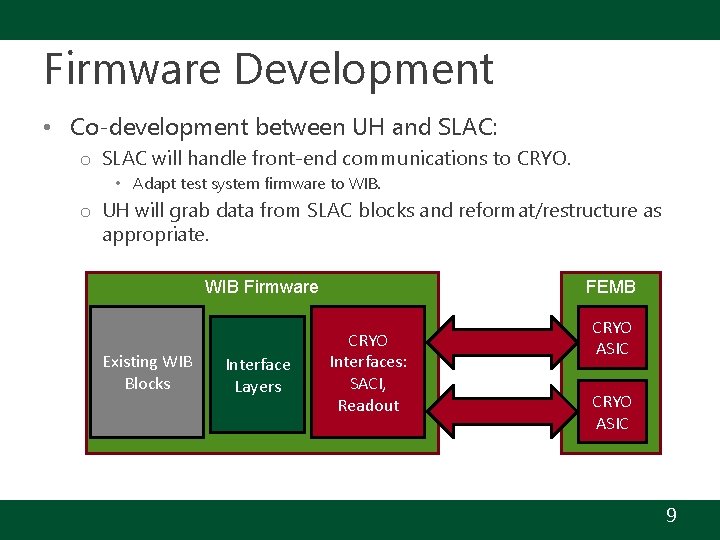
Firmware Development • Co-development between UH and SLAC: o SLAC will handle front-end communications to CRYO. • Adapt test system firmware to WIB. o UH will grab data from SLAC blocks and reformat/restructure as appropriate. WIB Firmware Existing WIB Blocks Interface Layers FEMB CRYO Interfaces: SACI, Readout CRYO ASIC 9
Schedule and Testing • FEMB design pending final packaging & pinout. • Possible milestones, assuming August submission: o Late August: schematic design complete. • Could be earlier if packaging is finalized. o November: first iteration into fab (~3 x FEMB). o End of year: testing with CRYO on new FEMB. • Assuming ASICs arrive ~Nov. , and that some experience from SLAC testing can be quickly adapted. o January/February: second iteration into fab (~16 x FEMB). o Warm and cold tests then occur in Hawaii. . . • Requires WIB and cryogenic test system. • Would be through WIB Gb. E, not DAQ. o Final delivery of FEMBs. 10
Summary • FEMBs for CRYO can be designed to work with slightly modified WIB for prototype testing. o Need to make sure modified WIB(s) can be made available to SLAC, UH. • FEMB will be designed at UH in close collaboration with SLAC. • Firmware for CRYO version of WIB will be developed jointly by SLAC & UH. • Testing planned primarily at UH. o Assuming cryogenic test system is made available to UH. 11

BACKUP 12
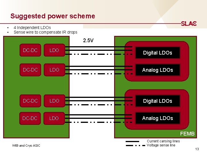
Suggested power scheme • • 4 Independent LDOs Sense wire to compensate IR drops 2. 5 V DC-DC LDO Digital LDOs DC-DC LDO Analog LDOs FEMB WIB and Cryo ASIC Current carrying lines Voltage sense line 13
- Slides: 13