Modern CPU Architecture With a View towards Meltdown


- Slides: 40

Modern CPU Architecture ----- With a View towards Meltdown and Spectre ---- Chris Lomont, Ph. D Jan 2018

Introduction: CPUs and Attacks Architecture We’ll use Intel CPUs as a specific architecture example. All modern large CPUs (AMD, IBM, ARM) work similarly. ->NEEDS Evolution Attacks Architecture needs (cache, speculative execution, security levels) have increased complexity tremendously as CPUs went from 4 to 8, 16, 32, and 64 bit data sizes. Complexity in CPU needs and features has driven exploits far into the corners of modern CPUs. Meltdown and Spectre are two large classes affecting nearly all modern, large processors as of 2018, affecting CPUs going back decades. ->COMPLEX ->BINGO! Free Power. Point Templates

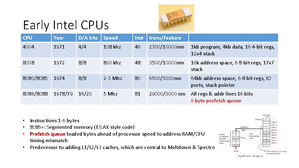
Early Intel CPUs CPU Year D/A bits Speed Inst trans/Feature 4004 1971 4/4 108 khz 46 2300/10000 nm 1 kb program, 4 kb data, 16 4 -bit regs, 12 x 4 stack 8008 1972 8/8 800 khz 48 3500/10000 nm 16 k address space, 6 8 -bit regs, 17 x 7 stack 8080/8085 1974 8/8 2 -3 Mhz 80 6500/3000 nm 64 kb address space, 6 -8 bit regs, IO ports, stack pointer 8086/8088 1978/79 16/20 5 Mhz 81 29000/3000 nm All regs & addr lines 16 bits 6 byte prefetch queue • Instructions 1 -6 bytes • 8086+: Segmented memory (ES: AX style code) • Prefetch queue loaded bytes ahead of processor speed to address RAM/CPU timing mismatch • Predecessor to adding L 1/L 2/L 3 caches, which are central to Meltdown & Spectre

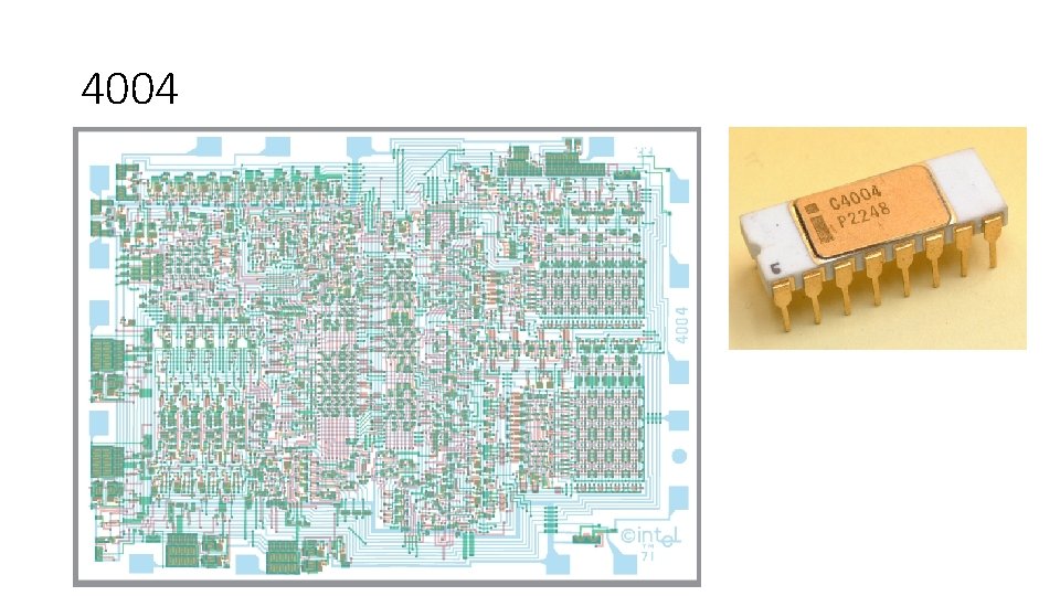
4004

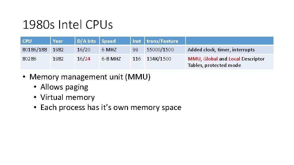
1980 s Intel CPUs CPU Year D/A bits Speed Inst trans/Feature 80186/188 1982 16/20 6 MHZ 99 55000/1500 Added clock, timer, interrupts 80286 1982 16/24 6 -8 MHZ 116 134 K/1500 MMU, Global and Local Descriptor Tables, protected mode • Memory management unit (MMU) • Allows paging • Virtual memory • Each process has it’s own memory space

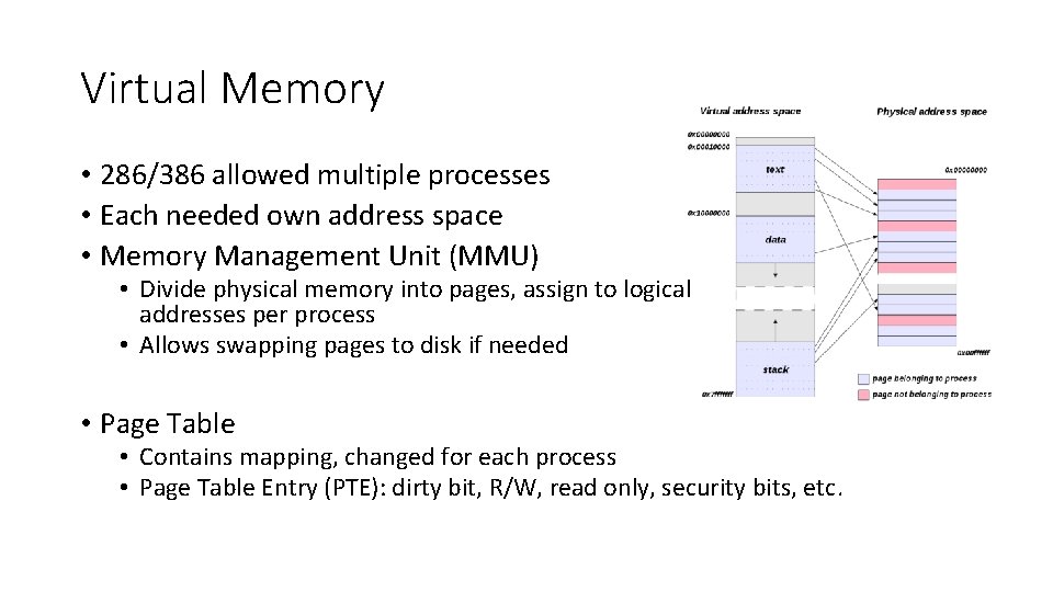
Virtual Memory • 286/386 allowed multiple processes • Each needed own address space • Memory Management Unit (MMU) • Divide physical memory into pages, assign to logical addresses per process • Allows swapping pages to disk if needed • Page Table • Contains mapping, changed for each process • Page Table Entry (PTE): dirty bit, R/W, read only, security bits, etc.

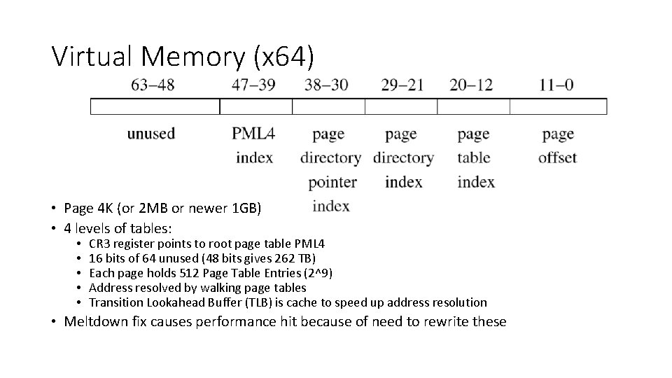
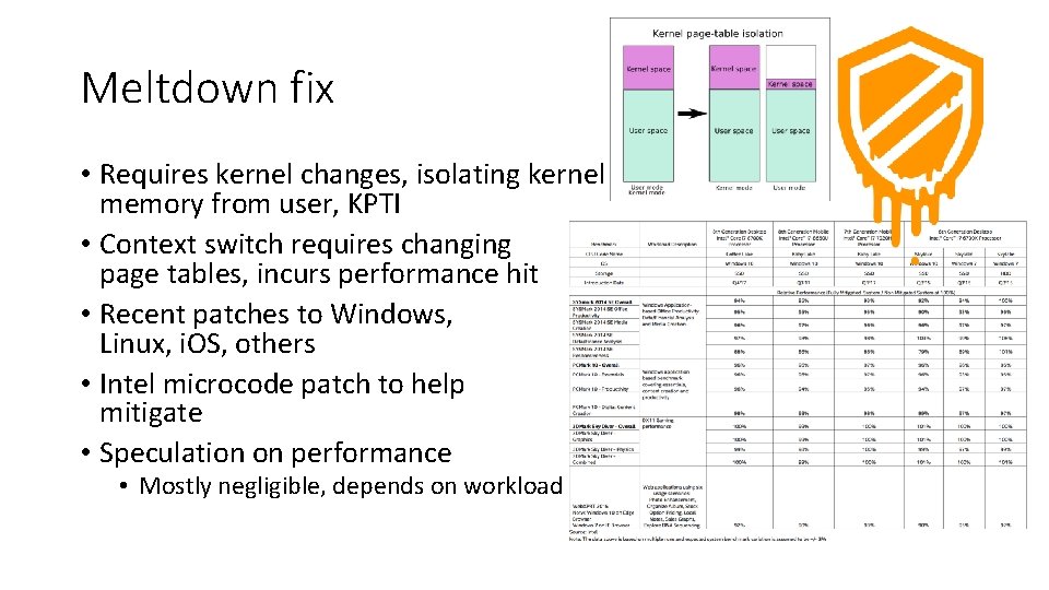
Virtual Memory (x 64) • Page 4 K (or 2 MB or newer 1 GB) • 4 levels of tables: • • • CR 3 register points to root page table PML 4 16 bits of 64 unused (48 bits gives 262 TB) Each page holds 512 Page Table Entries (2^9) Address resolved by walking page tables Transition Lookahead Buffer (TLB) is cache to speed up address resolution • Meltdown fix causes performance hit because of need to rewrite these

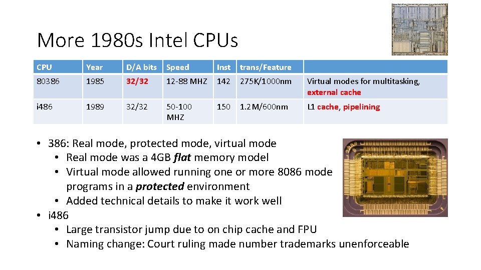
More 1980 s Intel CPUs CPU Year D/A bits Speed Inst trans/Feature 80386 1985 32/32 12 -88 MHZ 142 275 K/1000 nm Virtual modes for multitasking, external cache i 486 1989 32/32 50 -100 MHZ 150 1. 2 M/600 nm L 1 cache, pipelining • 386: Real mode, protected mode, virtual mode • Real mode was a 4 GB flat memory model • Virtual mode allowed running one or more 8086 mode programs in a protected environment • Added technical details to make it work well • i 486 • Large transistor jump due to on chip cache and FPU • Naming change: Court ruling made number trademarks unenforceable

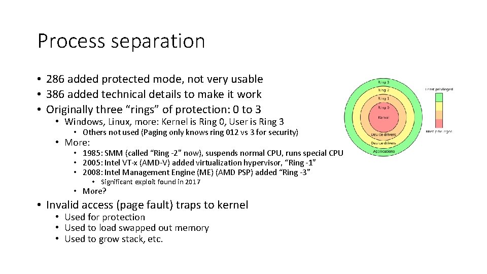
Process separation • 286 added protected mode, not very usable • 386 added technical details to make it work • Originally three “rings” of protection: 0 to 3 • Windows, Linux, more: Kernel is Ring 0, User is Ring 3 • Others not used (Paging only knows ring 012 vs 3 for security) • More: • 1985: SMM (called “Ring -2” now), suspends normal CPU, runs special CPU • 2005: Intel VT-x (AMD-V) added virtualization hypervisor, “Ring -1” • 2008: Intel Management Engine (ME) (AMD PSP) added “Ring -3” • Significant exploit found in 2017 • More? • Invalid access (page fault) traps to kernel • Used for protection • Used to load swapped out memory • Used to grow stack, etc.

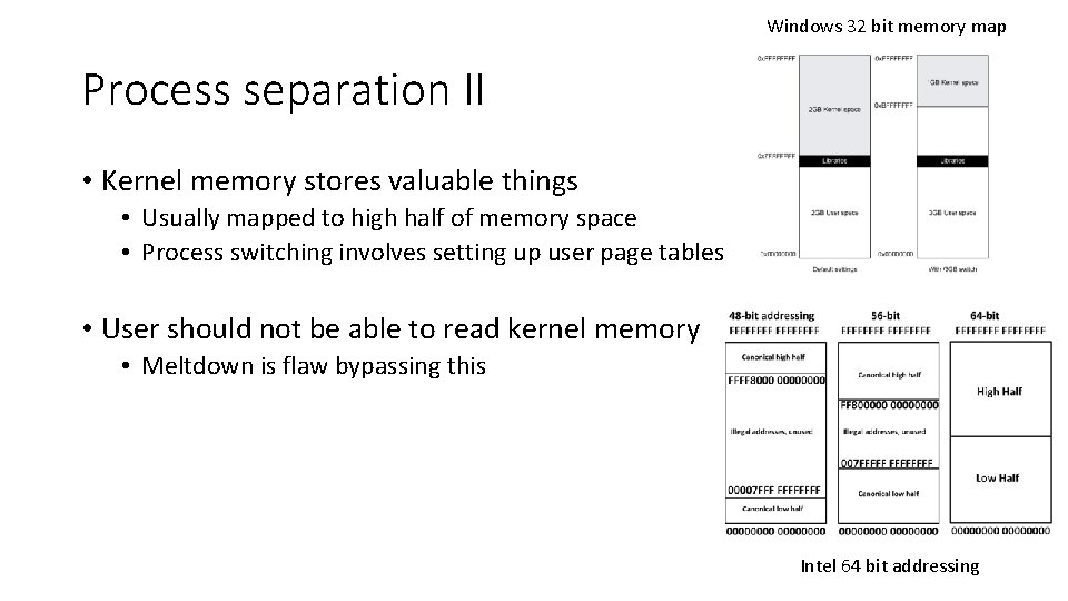
Windows 32 bit memory map Process separation II • Kernel memory stores valuable things • Usually mapped to high half of memory space • Process switching involves setting up user page tables • User should not be able to read kernel memory • Meltdown is flaw bypassing this Intel 64 bit addressing

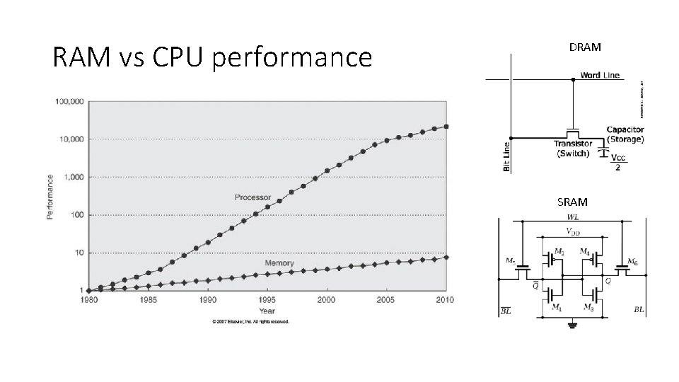
RAM vs CPU performance DRAM SRAM

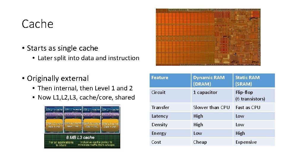
Cache • Starts as single cache • Later split into data and instruction • Originally external • Then internal, then Level 1 and 2 • Now L 1, L 2, L 3, cache/core, shared Feature Dynamic RAM (DRAM) Static RAM (SRAM) Circuit 1 capacitor Flip-flop (6 transistors) Transfer Slower than CPU Fast as CPU Latency High Low Density High Low Energy Low High Cost Cheap Expensive

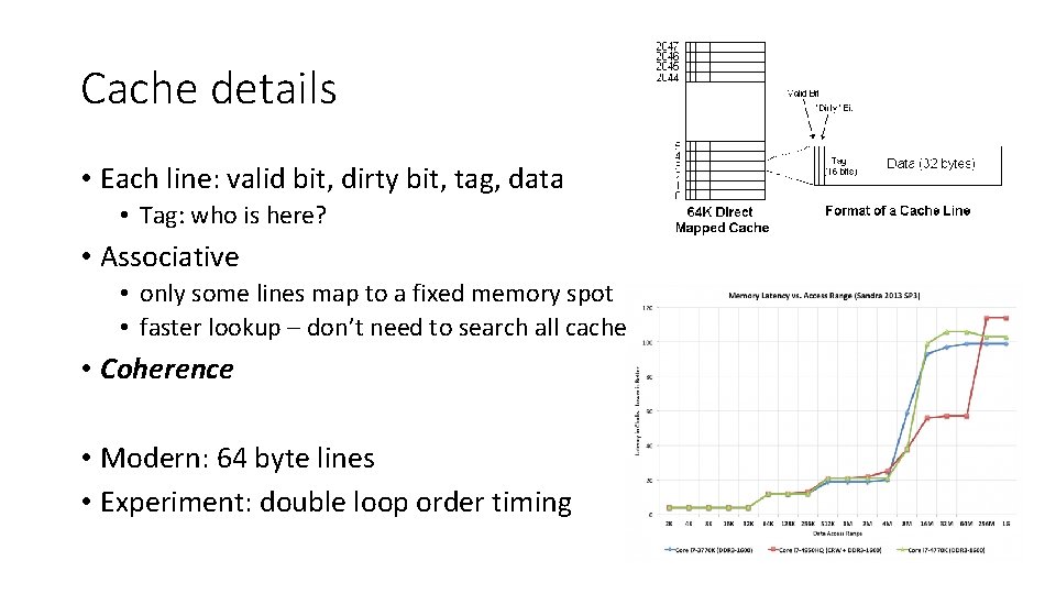
Cache details • Each line: valid bit, dirty bit, tag, data • Tag: who is here? • Associative • only some lines map to a fixed memory spot • faster lookup – don’t need to search all cache • Coherence • Modern: 64 byte lines • Experiment: double loop order timing

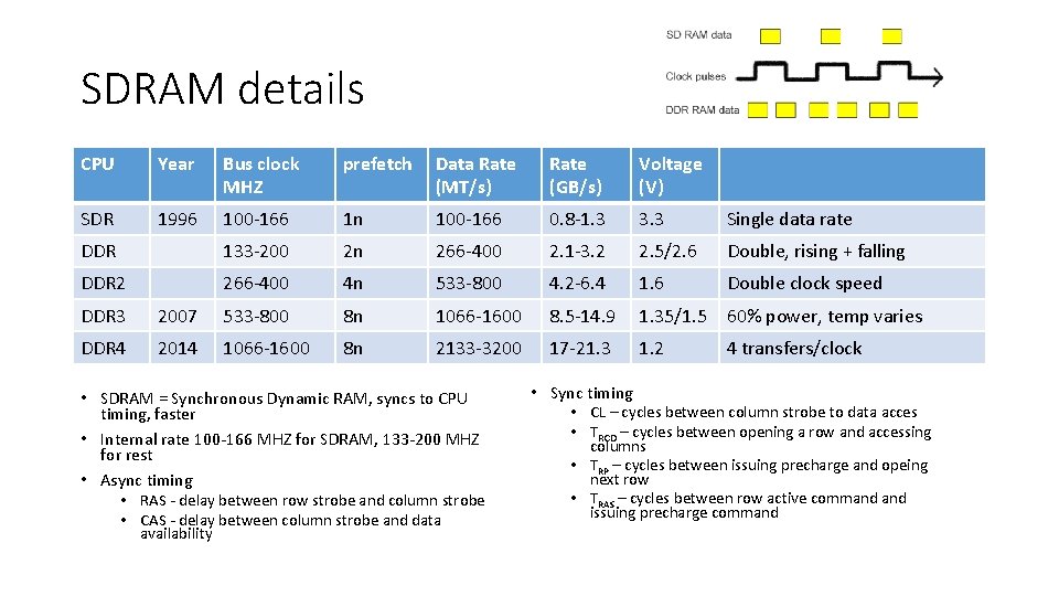
SDRAM details CPU Year Bus clock MHZ prefetch Data Rate (MT/s) Rate (GB/s) Voltage (V) SDR 1996 100 -166 1 n 100 -166 0. 8 -1. 3 3. 3 Single data rate DDR 133 -200 2 n 266 -400 2. 1 -3. 2 2. 5/2. 6 Double, rising + falling DDR 2 266 -400 4 n 533 -800 4. 2 -6. 4 1. 6 Double clock speed DDR 3 2007 533 -800 8 n 1066 -1600 8. 5 -14. 9 1. 35/1. 5 60% power, temp varies DDR 4 2014 1066 -1600 8 n 2133 -3200 17 -21. 3 1. 2 • SDRAM = Synchronous Dynamic RAM, syncs to CPU timing, faster • Internal rate 100 -166 MHZ for SDRAM, 133 -200 MHZ for rest • Async timing • RAS - delay between row strobe and column strobe • CAS - delay between column strobe and data availability • Sync timing 4 transfers/clock • CL – cycles between column strobe to data acces • TRCD – cycles between opening a row and accessing columns • TRP – cycles between issuing precharge and opeing next row • TRAS – cycles between row active command issuing precharge command

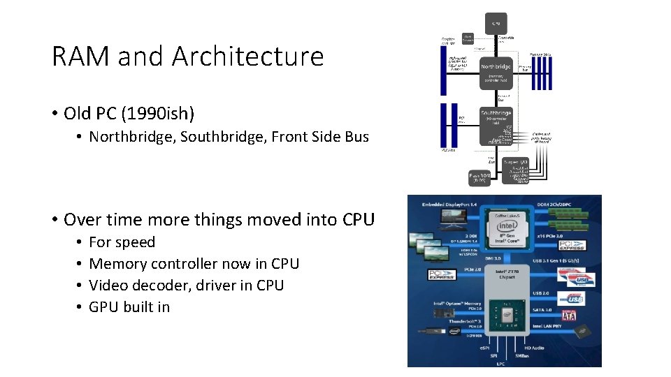
RAM and Architecture • Old PC (1990 ish) • Northbridge, Southbridge, Front Side Bus • Over time more things moved into CPU • • For speed Memory controller now in CPU Video decoder, driver in CPU GPU built in

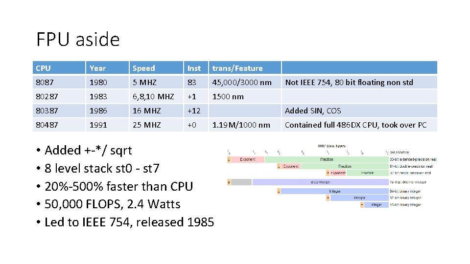
FPU aside CPU Year Speed Inst trans/Feature 8087 1980 5 MHZ 83 45, 000/3000 nm 80287 1983 6, 8, 10 MHZ +1 1500 nm 80387 1986 16 MHZ +12 80487 1991 25 MHZ +0 Not IEEE 754, 80 bit floating non std Added SIN, COS 1. 19 M/1000 nm • Added +-*/ sqrt • 8 level stack st 0 - st 7 • 20%-500% faster than CPU • 50, 000 FLOPS, 2. 4 Watts • Led to IEEE 754, released 1985 Contained full 486 DX CPU, took over PC

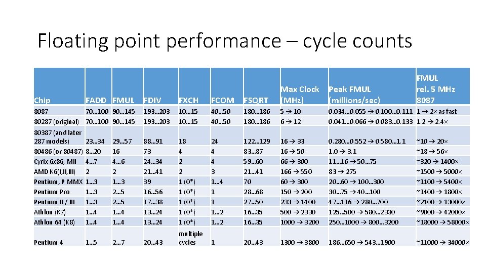
Floating point performance – cycle counts FDIV FXCH FCOM FSQRT Max Clock (MHz) 8087 70… 100 90… 145 80287 (original) 70… 100 90… 145 193… 203 10… 15 40… 50 180… 186 5 → 10 6 → 12 0. 034… 0. 055 → 0. 100… 0. 111 1 → 2× as fast 0. 041… 0. 066 → 0. 083… 0. 133 1. 2 → 2. 4× 80387 (and later 287 models) 23… 34 80486 (or 80487) 8… 20 Cyrix 6 x 86, MII 4… 7 AMD K 6(I, III) 2 Pentium, P MMX 1… 3 Pentium Pro 1… 3 Pentium II / III 1… 3 Athlon (K 7) 1… 4 Athlon 64 (K 8) 1… 4 88… 91 73 24… 34 21… 41 39 16… 56 17… 38 13… 24 18 4 2 2 1 (0*) 1 (0*) 24 4 4 3 1… 4 1 1 1… 2 122… 129 83… 87 59… 60 21… 41 70 28… 68 27… 50 16… 35 16 → 33 16 → 50 66 → 300 166 → 550 60 → 300 150 → 200 233 → 1400 500 → 2330 1000 → 3200 0. 280… 0. 552 → 0. 580… 1. 1 1. 0 → 3. 1 11… 16 → 50… 75 83 → 275 20… 60 → 100… 300 30… 75 → 40… 100 47… 116 → 280… 700 125… 500 → 580… 2330 250… 1000 → 800… 3200 ~10 → 20× ~18 → 56× ~320 → 1400× ~1500 → 5000× ~1100 → 5400× ~1400 → 1800× ~2100 → 13000× ~9000 → 42000× ~18000 → 58000× 20… 43 multiple cycles 1 20… 43 1300 → 3800 186… 650 → 543… 1900 ~11000 → 34000× Chip Pentium 4 FADD FMUL 1… 5 29… 57 16 4… 6 2 1… 3 2… 5 1… 4 2… 7 Peak FMUL (millions/sec) FMUL rel. 5 MHz 8087

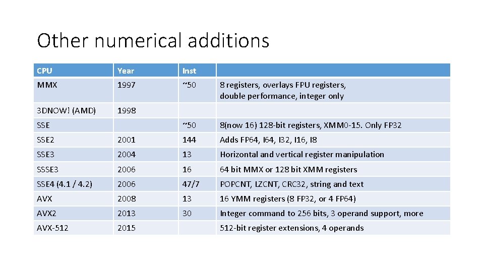
Other numerical additions CPU Year Inst MMX 1997 ~50 8 registers, overlays FPU registers, double performance, integer only 3 DNOW! (AMD) 1998 ~50 8(now 16) 128 -bit registers, XMM 0 -15. Only FP 32 SSE 2 2001 144 Adds FP 64, I 32, I 16, I 8 SSE 3 2004 13 Horizontal and vertical register manipulation SSSE 3 2006 16 64 bit MMX or 128 bit XMM registers SSE 4 (4. 1 / 4. 2) 2006 47/7 POPCNT, LZCNT, CRC 32, string and text AVX 2008 13 16 YMM registers (8 FP 32, or 4 FP 64) AVX 2 2013 30 Integer command to 256 bits, 3 operand support, more AVX-512 2015 512 -bit register extensions, 4 operands

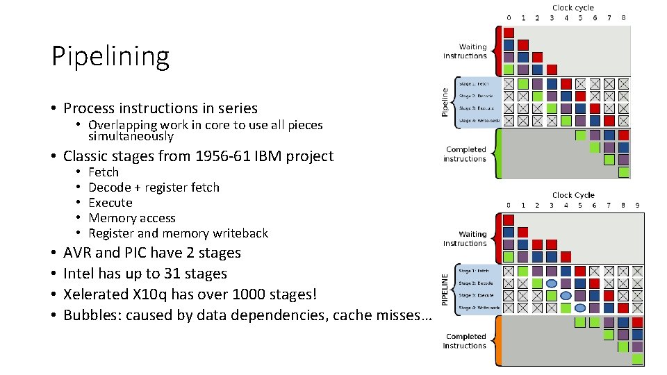
Pipelining • Process instructions in series • Overlapping work in core to use all pieces simultaneously • Classic stages from 1956 -61 IBM project • • • Fetch Decode + register fetch Execute Memory access Register and memory writeback AVR and PIC have 2 stages Intel has up to 31 stages Xelerated X 10 q has over 1000 stages! Bubbles: caused by data dependencies, cache misses…

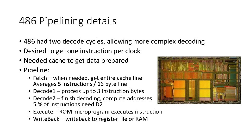
486 Pipelining details • 486 had two decode cycles, allowing more complex decoding • Desired to get one instruction per clock • Needed cache to get data prepared • Pipeline: • Fetch – when needed, get entire cache line Averages 5 instructions / 16 byte line • Decode 1 – process up to 3 instruction bytes • Decode 2 – finish decoding, compute addresses 5 % of instructions need D 2 • Execute – ROM microprogram executes instruction • Write. Back – writeback to register file or RAM

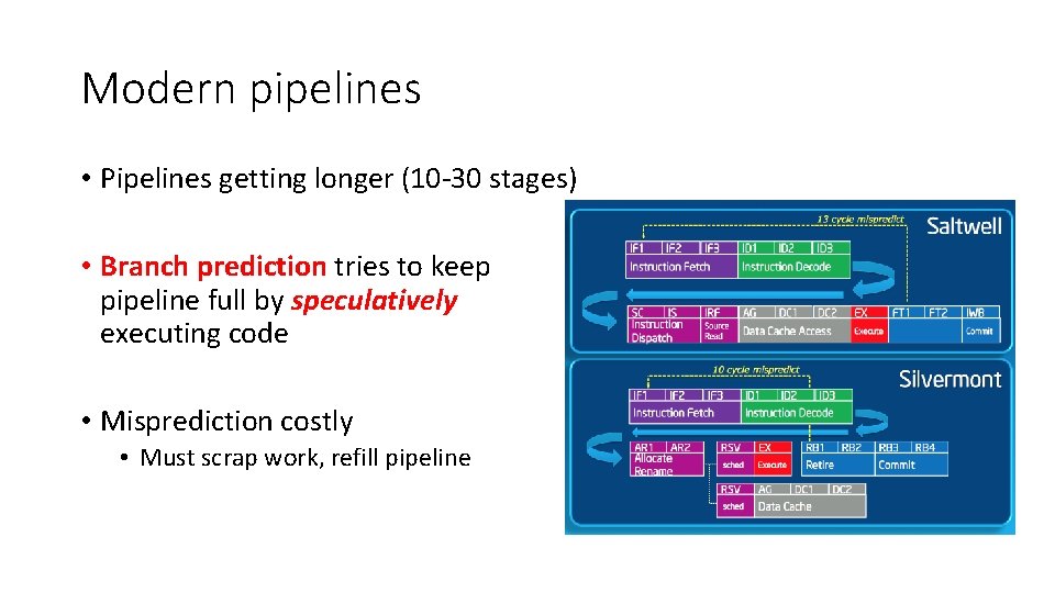
Modern pipelines • Pipelines getting longer (10 -30 stages) • Branch prediction tries to keep pipeline full by speculatively executing code • Misprediction costly • Must scrap work, refill pipeline

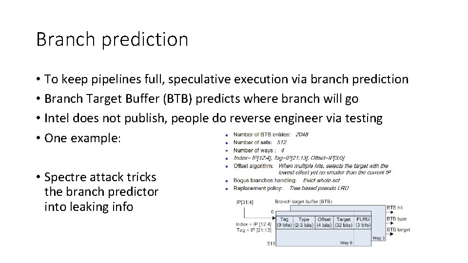
Branch prediction • To keep pipelines full, speculative execution via branch prediction • Branch Target Buffer (BTB) predicts where branch will go • Intel does not publish, people do reverse engineer via testing • One example: • Spectre attack tricks the branch predictor into leaking info

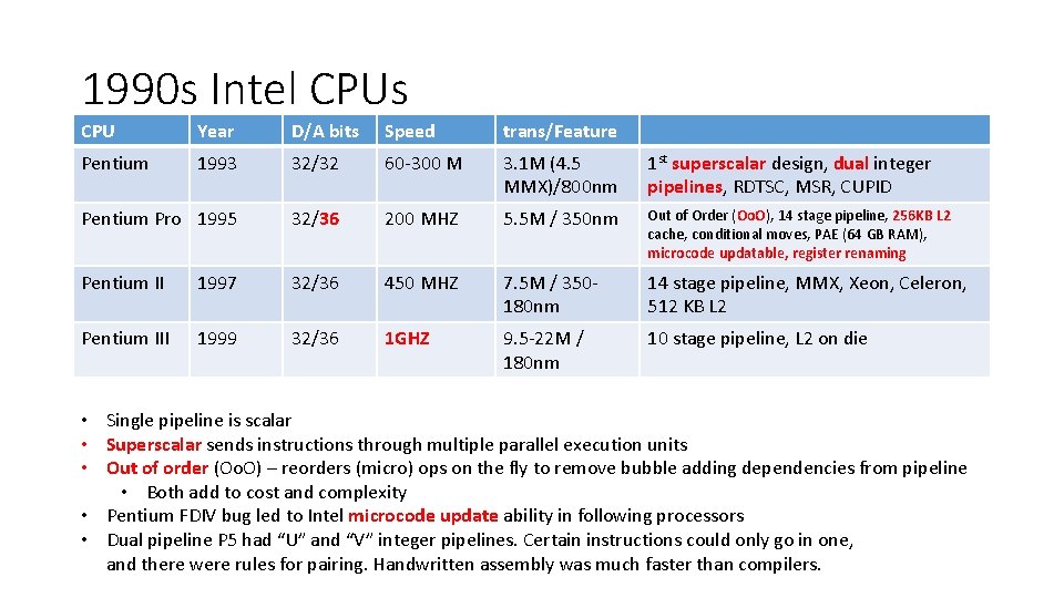
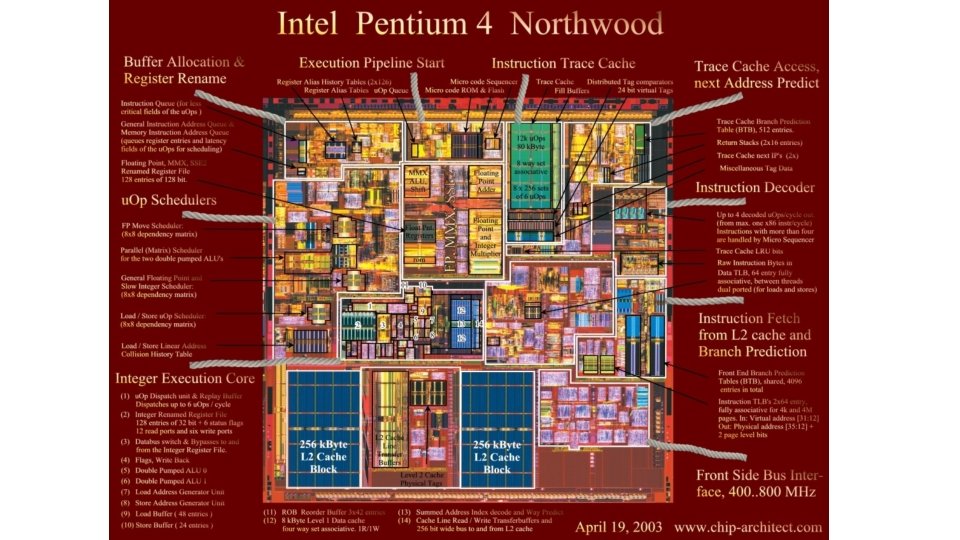
1990 s Intel CPUs CPU Year D/A bits Speed trans/Feature Pentium 1993 32/32 60 -300 M 3. 1 M (4. 5 MMX)/800 nm 1 st superscalar design, dual integer pipelines, RDTSC, MSR, CUPID Pentium Pro 1995 32/36 200 MHZ 5. 5 M / 350 nm Out of Order (Oo. O), 14 stage pipeline, 256 KB L 2 cache, conditional moves, PAE (64 GB RAM), microcode updatable, register renaming Pentium II 1997 32/36 450 MHZ 7. 5 M / 350180 nm 14 stage pipeline, MMX, Xeon, Celeron, 512 KB L 2 Pentium III 1999 32/36 1 GHZ 9. 5 -22 M / 180 nm 10 stage pipeline, L 2 on die • Single pipeline is scalar • Superscalar sends instructions through multiple parallel execution units • Out of order (Oo. O) – reorders (micro) ops on the fly to remove bubble adding dependencies from pipeline • Both add to cost and complexity • Pentium FDIV bug led to Intel microcode update ability in following processors • Dual pipeline P 5 had “U” and “V” integer pipelines. Certain instructions could only go in one, and there were rules for pairing. Handwritten assembly was much faster than compilers.

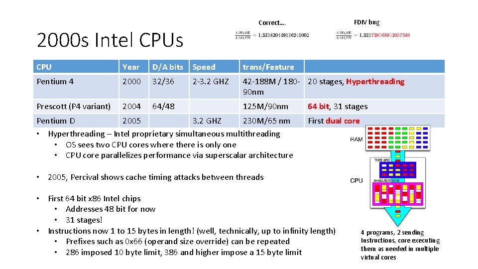
FDIV bug Correct…. 2000 s Intel CPUs CPU Year D/A bits Speed trans/Feature Pentium 4 2000 32/36 2 -3. 2 GHZ 42 -188 M / 180 - 20 stages, Hyperthreading 90 nm Prescott (P 4 variant) 2004 64/48 125 M/90 nm Pentium D 2005 3. 2 GHZ 230 M/65 nm • Hyperthreading – Intel proprietary simultaneous multithreading • OS sees two CPU cores where there is only one • CPU core parallelizes performance via superscalar architecture 64 bit, 31 stages First dual core • 2005, Percival shows cache timing attacks between threads • First 64 bit x 86 Intel chips • Addresses 48 bit for now • 31 stages! • Instructions now 1 to 15 bytes in length! (well, technically, up to infinity length) • Prefixes such as 0 x 66 (operand size override) can be repeated • 286 imposed 10 byte limit, 386 and higher impose a 15 byte limit 4 programs, 2 sending Instructions, core executing them as needed in multiple virtual cores


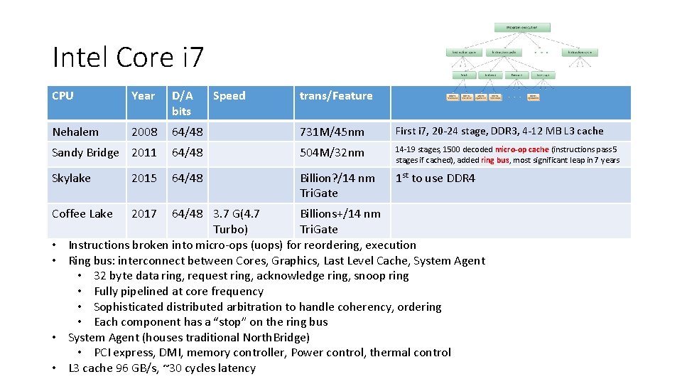
Intel Core i 7 CPU Year D/A bits Nehalem 2008 64/48 731 M/45 nm First i 7, 20 -24 stage, DDR 3, 4 -12 MB L 3 cache Sandy Bridge 2011 64/48 504 M/32 nm 14 -19 stages, 1500 decoded micro-op cache (instructions pass 5 stages if cached), added ring bus, most significant leap in 7 years Skylake 2015 64/48 Billion? /14 nm Tri. Gate 1 st to use DDR 4 Coffee Lake 2017 • • Speed trans/Feature 64/48 3. 7 G(4. 7 Billions+/14 nm Turbo) Tri. Gate Instructions broken into micro-ops (uops) for reordering, execution Ring bus: interconnect between Cores, Graphics, Last Level Cache, System Agent • 32 byte data ring, request ring, acknowledge ring, snoop ring • Fully pipelined at core frequency • Sophisticated distributed arbitration to handle coherency, ordering • Each component has a “stop” on the ring bus System Agent (houses traditional North. Bridge) • PCI express, DMI, memory controller, Power control, thermal control L 3 cache 96 GB/s, ~30 cycles latency

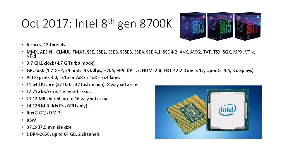
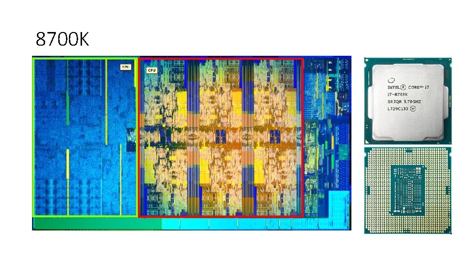
Oct 2017: Intel 8 th gen 8700 K • 6 cores, 12 threads • MMX, AES-NI, CLMUL, FMA 3, SSE 2, SSE 3, SSE 4, SSE 4. 1, SSE 4. 2, AVX 2, TXT, TSX, SGX, MPX, VT-x, VT-d • 3. 7 GHZ clock (4. 7 G Turbo mode) • GPU 630 (1. 2 GHZ, 24 units, 4 K 60 fps, H 265, VP 9, DP 1. 2, HDMI 2. 0, HDCP 2. 2, Directx 12, Open. GL 4. 5, 3 displays) • PCI Express 3. 0, 1 x 16 or 2 x 8 or 1 x 8 + 2 x 4 lanes • L 1 64 k. B/core (32 Data, 32 Instruction), 8 way set assoc • L 2 256 k. B/core, 4 way set assoc • L 3 12 MB shared, up to 16 way set assoc • L 4 128 Mi. B (Iris Pro GPU only) • Bus 8 GT/s DMI 3 • 95 W • 37. 5 x 37. 5 mm die size • DDR 4 -2666, up to 64 GB, 2 channels

8700 K


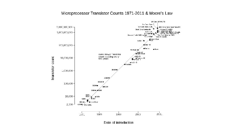
End of Moore’s law? • Plenty of good, accurate articles • Scientific American, Wired • Physics: • • • 1985: 1000 nm feature 2018: 14 nm feature Silicon atom: 0. 2 nm Quantum mechanics: smaller features “fuzzier” 5 GHZ: light travels 6 cm per clock tick, electricity ~80% of this in wire. • Cannot have RAM too far from CPU • CPU Die size ~ 400 mm^2, so light speed an issue for higher clocks • Heat hard to remove, so lower voltage, moving to diamond substrates, etc… • Economics • $8 B for current fab plant.

Meltdown and Spectre • 20 year old flaws in many, many chips, • Intel, ARM, AMD, IBM, more • Found by researchers from four teams during 2017 • Intel, Google, Amazon, AMD, Microsoft, Apple, others working behind closed doors to fix • Publicly disclosed early Jan 2018 • Biggest chip security flaw probably ever • Will likely cost billions in liability for many companies • Technical read: https: //googleprojectzero. blogspot. com/

Meltdown • “Melts” boundaries between hardware enforced security layers • User mode programs can read kernel mode data. • Affects: • Software: Windows, Linux, i. OS, mac. OS, cloud services, Android, others • Hardware: Intel x 86/64, most ARM, IBM Power, others • Not affected: CPUs not doing speculative execution • Many Qualcomm, some ARM, Raspberry Pi • Not hard to do. • CVE-2017 -5754 : rogue data cache load

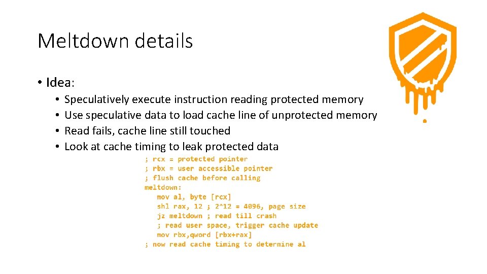
Meltdown details • Idea: • • Speculatively execute instruction reading protected memory Use speculative data to load cache line of unprotected memory Read fails, cache line still touched Look at cache timing to leak protected data

Meltdown fix • Requires kernel changes, isolating kernel memory from user, KPTI • Context switch requires changing page tables, incurs performance hit • Recent patches to Windows, Linux, i. OS, others • Intel microcode patch to help mitigate • Speculation on performance • Mostly negligible, depends on workload

Spectre • Breaks the isolation between applications • Attacker can trick error-free programs into leaking their secrets • Affects: • Software: Windows, Linux, i. OS, mac. OS, cloud services, Android, others • Hardware: Intel x 86/64, AMD, most ARM, IBM Power, others • Not affected: CPUs not doing speculative execution • Many Qualcomm, some ARM, Raspberry Pi • Hard to exploit, but also much harder to fix than meltdown. • Requires careful code analysis and recompilation • CVE-2017 -5753 : bounds check bypass • CVE-2017 -5715 : branch target injection

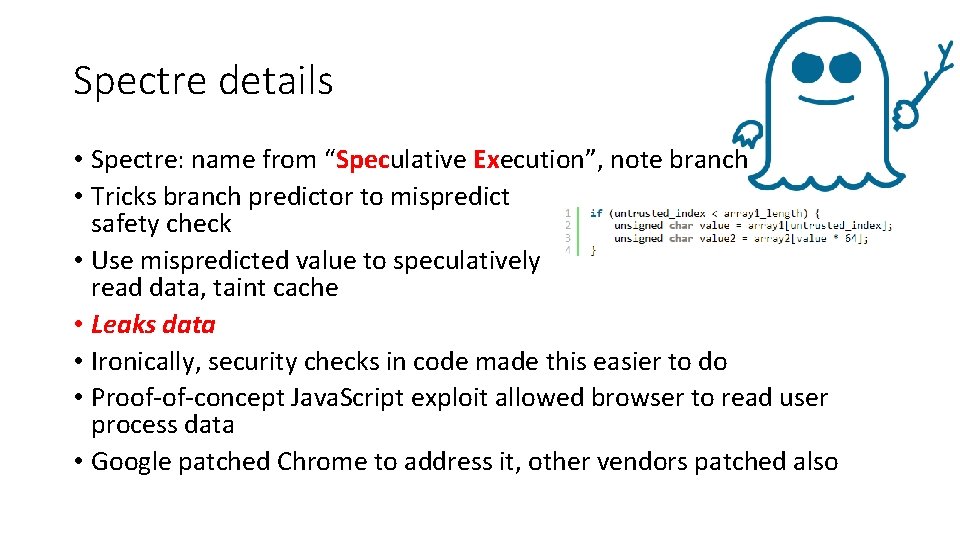
Spectre details • Spectre: name from “Speculative Execution”, note branch • Tricks branch predictor to mispredict safety check • Use mispredicted value to speculatively read data, taint cache • Leaks data • Ironically, security checks in code made this easier to do • Proof-of-concept Java. Script exploit allowed browser to read user process data • Google patched Chrome to address it, other vendors patched also

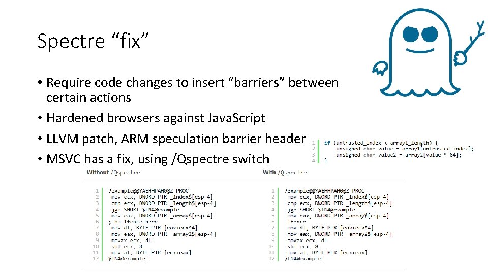
Spectre “fix” • Require code changes to insert “barriers” between certain actions • Hardened browsers against Java. Script • LLVM patch, ARM speculation barrier header • MSVC has a fix, using /Qspectre switch

Vendor Fixes • Intel • Working on mitigations via microcode updates • Apple • i. OS, mac. OS High Sierre, tv. OS, Safari on Sierra and El Capitan • Addresses Meltdown, Spectre to some extent • Microsoft • Windows 10, 8, Server 2012, Windows 7, Windows Server 2008 • X 64 only? • Meltdown and Spectre variant 1 only, not variant 2 • Google • Pushing “retpoline” binary modification to others to mitigate Spectre • Amazon • Rolled out new, slower virtual machine infrastructure. • Linux • Patches to 4. 4 and 4. 9 trees • Addresses Meltdown only • Many others

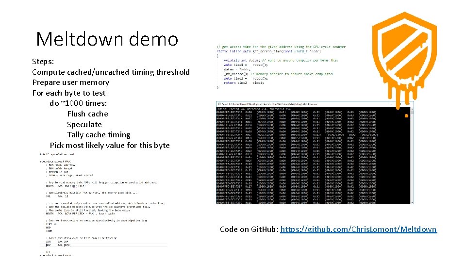
Meltdown demo Steps: Compute cached/uncached timing threshold Prepare user memory For each byte to test do ~1000 times: Flush cache Speculate Tally cache timing Pick most likely value for this byte Code on Git. Hub: https: //github. com/Chris. Lomont/Meltdown

Questions?