Modeling dislocation effects on electronic and optical properties

- Slides: 50

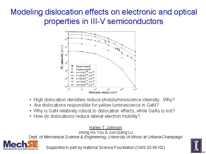
Modeling dislocation effects on electronic and optical properties in III-V semiconductors • • High dislocation densities reduce photoluminescence intensity. Why? Are dislocations responsible for yellow luminescence in Ga. N? Why is Ga. N relatively robust to dislocation effects, while Ga. As is not? How do dislocations reduce lateral electron mobility? Harley T. Johnson Jeong Ho You & Jun-Qiang Lu Dept. of Mechanical Science & Engineering, University of Illinois at Urbana-Champaign Supported in part by National Science Foundation (CMS 02 -96102)

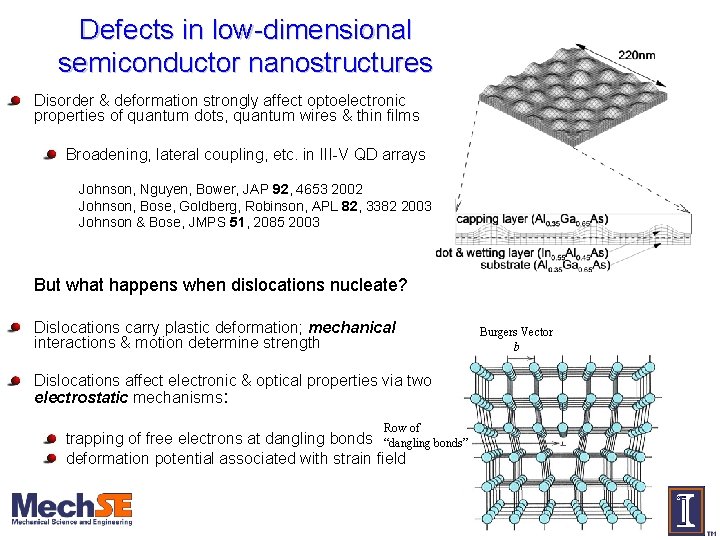
Defects in low-dimensional semiconductor nanostructures Disorder & deformation strongly affect optoelectronic properties of quantum dots, quantum wires & thin films Broadening, lateral coupling, etc. in III-V QD arrays Johnson, Nguyen, Bower, JAP 92, 4653 2002 Johnson, Bose, Goldberg, Robinson, APL 82, 3382 2003 Johnson & Bose, JMPS 51, 2085 2003 But what happens when dislocations nucleate? Dislocations carry plastic deformation; mechanical interactions & motion determine strength Dislocations affect electronic & optical properties via two electrostatic mechanisms: Row of trapping of free electrons at dangling bonds “dangling bonds” deformation potential associated with strain field Burgers Vector b

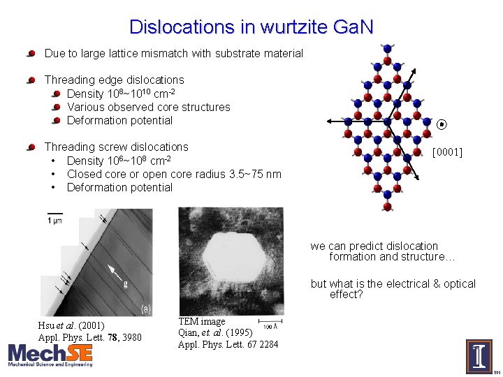
Dislocations in wurtzite Ga. N Due to large lattice mismatch with substrate material Threading edge dislocations Density 108~1010 cm-2 Various observed core structures Deformation potential Threading screw dislocations • Density 106~108 cm-2 • Closed core or open core radius 3. 5~75 nm • Deformation potential [0001] we can predict dislocation formation and structure… but what is the electrical & optical effect? Hsu et al. (2001) Appl. Phys. Lett. 78, 3980 TEM image Qian, et. al. (1995) Appl. Phys. Lett. 67 2284

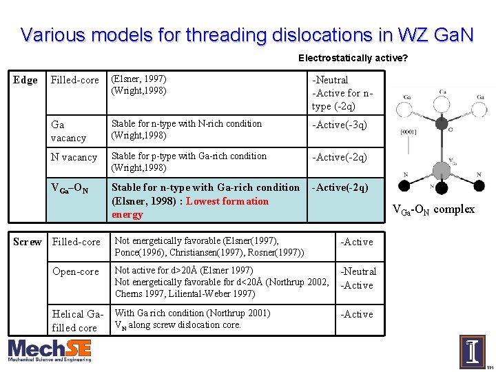
Various models for threading dislocations in WZ Ga. N Electrostatically active? Edge Filled-core (Elsner, 1997) (Wright, 1998) -Neutral -Active for ntype (-2 q) Ga vacancy Stable for n-type with N-rich condition (Wright, 1998) -Active(-3 q) N vacancy Stable for p-type with Ga-rich condition (Wright, 1998) -Active(-2 q) VGa–ON Stable for n-type with Ga-rich condition (Elsner, 1998) : Lowest formation energy -Active(-2 q) VGa-ON complex Not energetically favorable (Elsner(1997), Ponce(1996), Christiansen(1997), Rosner(1997)) -Active Open-core Not active for d>20Å (Elsner 1997) Not energetically favorable for d<20Å (Northrup 2002, Cherns 1997, Liliental-Weber 1997) -Neutral -Active Helical Gafilled core With Ga rich condition (Northrup 2001) VN along screw dislocation core. -Active Screw Filled-core

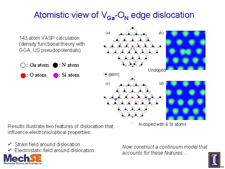
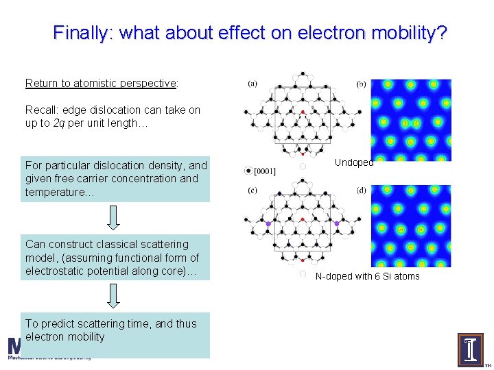
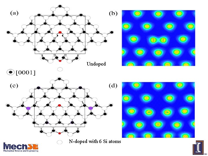
Atomistic view of VGa-ON edge dislocation 143 atom VASP calculation (density functional theory with GGA, US pseudopotentials) : Ga atom : N atom : O atom : Si atom Results illustrate two features of dislocation that influence electronic/optical properties: ü Strain field around dislocation ü Electrostatic field around dislocation Undoped N-doped with 6 Si atoms Now construct a continuum model that accounts for these features…

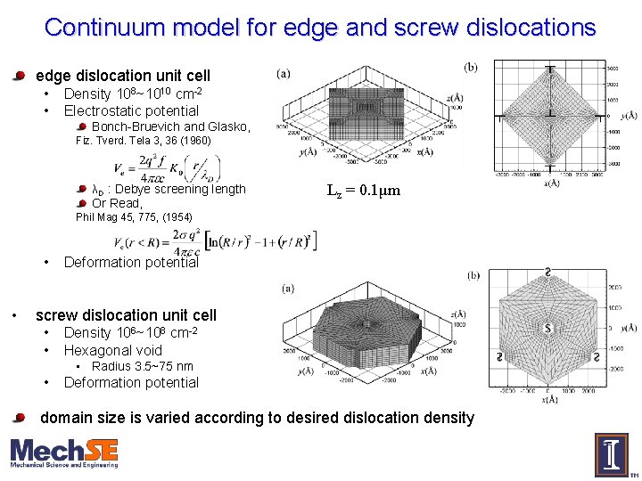
Continuum model for edge and screw dislocations edge dislocation unit cell • • Density 108~1010 cm-2 Electrostatic potential Bonch-Bruevich and Glasko, Fiz. Tverd. Tela 3, 36 (1960) λD : Debye screening length Or Read, Lz = 0. 1μm Phil Mag 45, 775, (1954) • • Deformation potential screw dislocation unit cell • • Density 106~108 cm-2 Hexagonal void • Radius 3. 5~75 nm • Deformation potential domain size is varied according to desired dislocation density

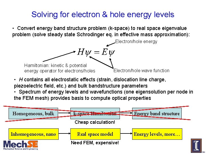
Solving for electron & hole energy levels • Convert energy band structure problem (k-space) to real space eigenvalue problem (solve steady state Schrodinger eq. in effective mass approximation): Electron/hole energy Hamiltonian: kinetic & potential energy operator for electrons/holes Electron/hole wave function • H contains all electrostatic effects (strain, dislocation line charge, piezoelectric field, etc. ) and bulk bandstructure parameters • Spectrum of energy levels and wavefunctions (one eigensolution per node in the FEM mesh) provides basis to compute optical properties Homogeneous, bulk k-space Hamiltonian Energy band structure Cheap calculation! Inhomogeneous, nano Real space model Need FEM, expensive! Energy levels, more…

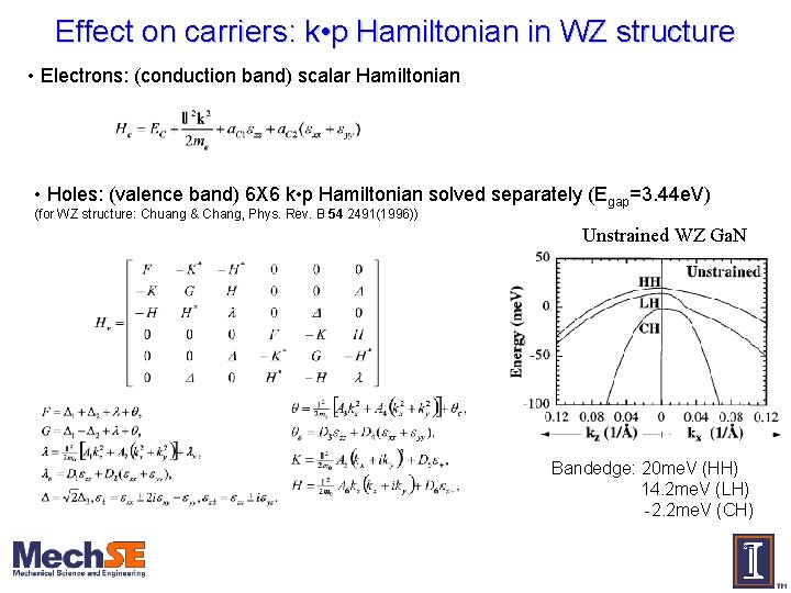
Effect on carriers: k • p Hamiltonian in WZ structure • Electrons: (conduction band) scalar Hamiltonian • Holes: (valence band) 6 X 6 k • p Hamiltonian solved separately (Egap=3. 44 e. V) (for WZ structure: Chuang & Chang, Phys. Rev. B 54 2491(1996)) Unstrained WZ Ga. N Bandedge: 20 me. V (HH) 14. 2 me. V (LH) -2. 2 me. V (CH)

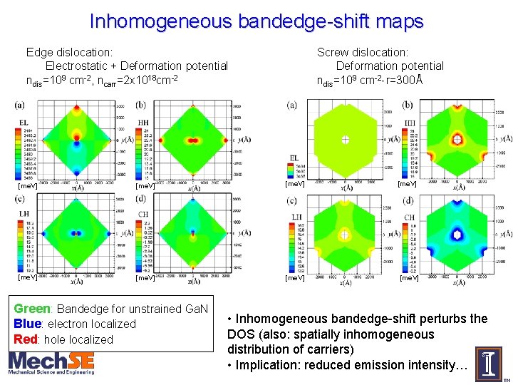
Inhomogeneous bandedge-shift maps Edge dislocation: Electrostatic + Deformation potential ndis=109 cm-2, ncarr=2 x 1018 cm-2 Screw dislocation: Deformation potential ndis=109 cm-2, r=300Å [me. V] [me. V] Green: Bandedge for unstrained Ga. N Blue: electron localized Red: hole localized • Inhomogeneous bandedge-shift perturbs the DOS (also: spatially inhomogeneous distribution of carriers) • Implication: reduced emission intensity…

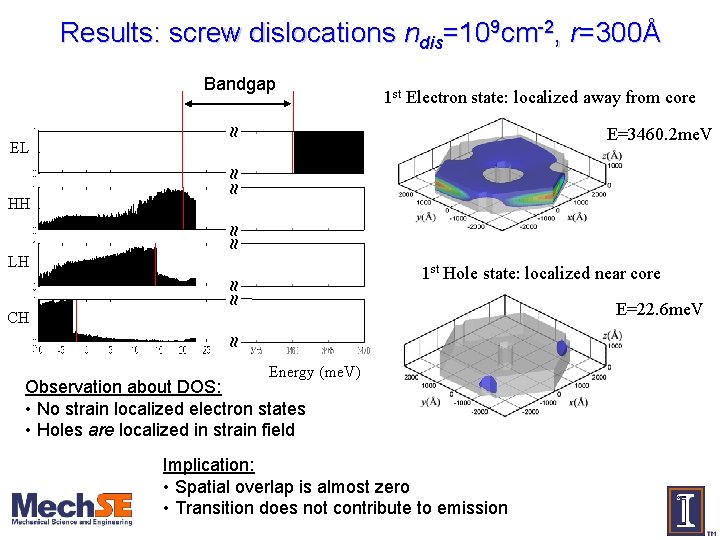
Results: screw dislocations ndis=109 cm-2, r=300Å Bandgap 1 st Electron state: localized away from core ~ ~ E=3460. 2 me. V ~ ~ ~~ EL ~ ~~ ~ HH LH ~ ~ ~~ 1 st Hole state: localized near core E=22. 6 me. V ~ ~ CH Energy (me. V) Observation about DOS: • No strain localized electron states • Holes are localized in strain field Implication: • Spatial overlap is almost zero • Transition does not contribute to emission

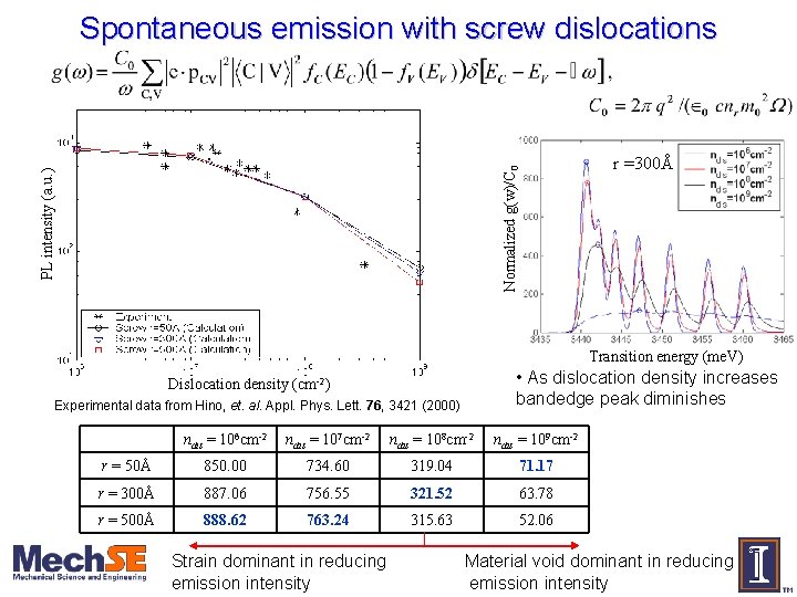
PL intensity (a. u. ) Normalized g(w)/C 0 Spontaneous emission with screw dislocations r =300Å Transition energy (me. V) • As dislocation density increases bandedge peak diminishes Dislocation density (cm-2) Experimental data from Hino, et. al. Appl. Phys. Lett. 76, 3421 (2000) ndis = 106 cm-2 ndis = 107 cm-2 ndis = 108 cm-2 ndis = 109 cm-2 r = 50Å 850. 00 734. 60 319. 04 71. 17 r = 300Å 887. 06 756. 55 321. 52 63. 78 r = 500Å 888. 62 763. 24 315. 63 52. 06 Strain dominant in reducing emission intensity Material void dominant in reducing emission intensity

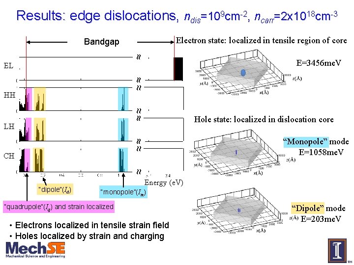
Results: edge dislocations, ndis=109 cm-2, ncarr=2 x 1018 cm-3 Electron state: localized in tensile region of core ~ ~ Bandgap E=3456 me. V ~ ~ ~~ EL ~ ~~ ~ HH ~ ~ ~~ LH “Monopole” mode E=1058 me. V ~ ~ CH Hole state: localized in dislocation core “dipole”(Id) Energy (e. V) “monopole”(Im) “quadrupole”(Iq) and strain localized • Electrons localized in tensile strain field • Holes localized by strain and charging “Dipole” mode E=203 me. V

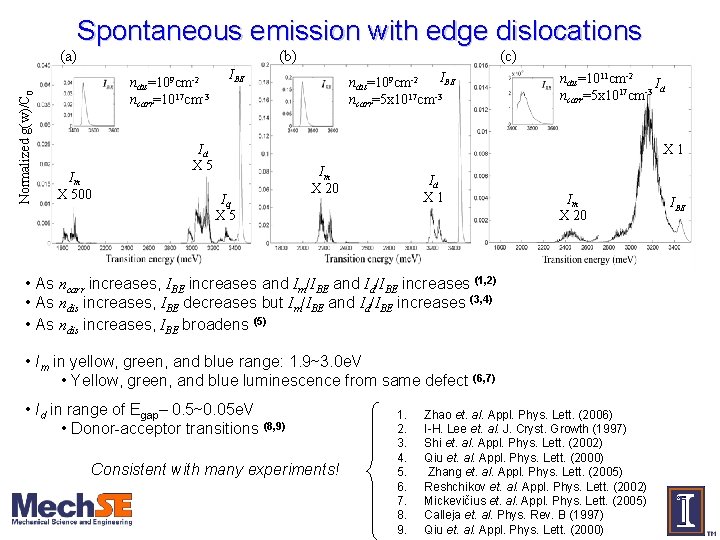
Normalized g(w)/C 0 (a) Spontaneous emission with edge dislocations (b) ndis=109 cm-2 ncarr=1017 cm-3 Im X 500 (c) IBE Id X 5 IBE ndis=109 cm-2 ncarr=5 x 1017 cm-3 ndis=1011 cm-2 Id ncarr=5 x 1017 cm-3 X 1 Iq X 5 Im X 20 Id X 1 Im X 20 • As ncarr increases, IBE increases and Im/IBE and Id/IBE increases (1, 2) • As ndis increases, IBE decreases but Im/IBE and Id/IBE increases (3, 4) • As ndis increases, IBE broadens (5) • Im in yellow, green, and blue range: 1. 9~3. 0 e. V • Yellow, green, and blue luminescence from same defect (6, 7) • Id in range of Egap– 0. 5~0. 05 e. V • Donor-acceptor transitions (8, 9) Consistent with many experiments! 1. 2. 3. 4. 5. 6. 7. 8. 9. Zhao et. al. Appl. Phys. Lett. (2006) I-H. Lee et. al. J. Cryst. Growth (1997) Shi et. al. Appl. Phys. Lett. (2002) Qiu et. al. Appl. Phys. Lett. (2000) Zhang et. al. Appl. Phys. Lett. (2005) Reshchikov et. al. Appl. Phys. Lett. (2002) Mickevičius et. al. Appl. Phys. Lett. (2005) Calleja et. al. Phys. Rev. B (1997) Qiu et. al. Appl. Phys. Lett. (2000) IBE

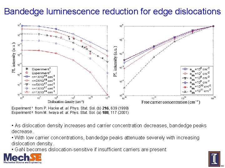
Bandedge luminescence reduction for edge dislocations Experiment 1 from P. Hacke et. al. Phys. Stat. Sol. (b) 216, 639 (1999) Experiment 2 from M. Iwaya et. al. Phys. Stat. Sol. (a) 188, 117 (2001) • As dislocation density increases and carrier concentration decreases, bandedge peaks decrease. • With low carrier concentrations, bandedge peaks attenuate severely with increasing dislocation density. • Ga. N becomes dislocation-sensitive if insufficient carriers are present

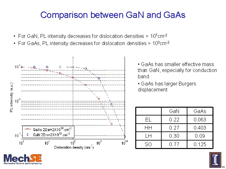
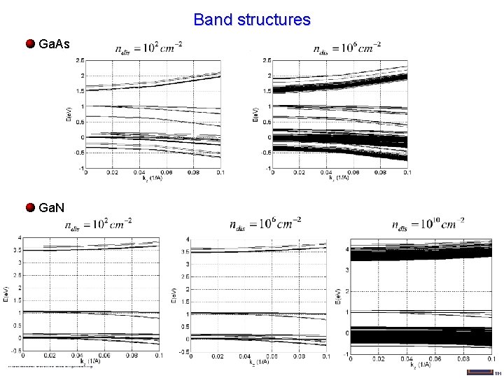
Comparison between Ga. N and Ga. As • For Ga. N, PL intensity decreases for dislocation densities > 107 cm-2 • For Ga. As, PL intensity decreases for dislocation densities > 103 cm-2 • Ga. As has smaller effective mass than Ga. N, especially for conduction band • Ga. As has larger Burgers displacement Ga. N Ga. As EL 0. 22 0. 063 HH 0. 27 0. 403 LH 0. 30 0. 09 SO 0. 77 0. 125

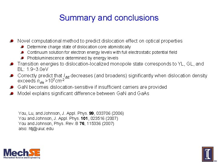
Summary and conclusions Novel computational method to predict dislocation effect on optical properties Determine charge state of dislocation core atomistically Continuum solution for electron energy levels with full electrostatic potential field Photoluminescence determined by energy levels Transition energies to dislocation-localized monopole state corresponds to YL, GL, and BL: 1. 9~3. 0 e. V Correctly predict that IBE decreases (and broadens) significantly when dislocation density exceeds ndis >107 cm-2 Ga. N becomes dislocation-sensitive if insufficient carriers are provided Model explains significant difference between Ga. N and Ga. As You, Lu, and Johnson, J. Appl. Phys. 99, 033706 (2006) You and Johnson, J. Appl. Phys. 101, 023516 (2007) You and Johnson, Phys. Rev. B 76, 115336 (2007) also: htj@uiuc. edu


Finally: what about effect on electron mobility? Return to atomistic perspective: Recall: edge dislocation can take on up to 2 q per unit length… For particular dislocation density, and given free carrier concentration and temperature… Can construct classical scattering model, (assuming functional form of electrostatic potential along core)… To predict scattering time, and thus electron mobility Undoped N-doped with 6 Si atoms

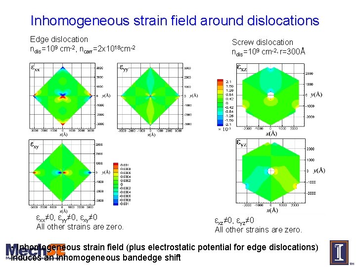
Inhomogeneous strain field around dislocations Edge dislocation ndis=109 cm-2, ncarr=2 x 1018 cm-2 εxx≠ 0, εyy≠ 0, εxy≠ 0 All other strains are zero. Screw dislocation ndis=109 cm-2, r=300Å εxz≠ 0, εyz≠ 0 All other strains are zero. • Inhomogeneous strain field (plus electrostatic potential for edge dislocations) induces an inhomogeneous bandedge shift

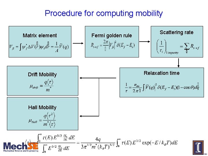
Procedure for computing mobility Matrix element Drift Mobility Hall Mobility Fermi golden rule Scattering rate Relaxation time

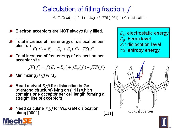
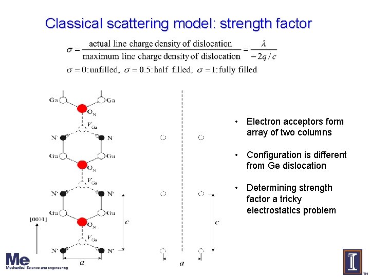
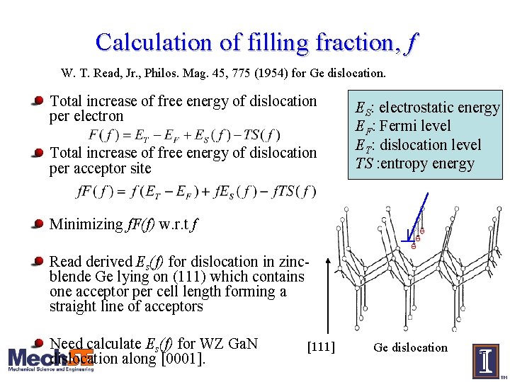
Calculation of filling fraction, f W. T. Read, Jr. , Philos. Mag. 45, 775 (1954) for Ge dislocation. Electron acceptors are NOT always fully filled. Total increase of free energy of dislocation per electron ES: electrostatic energy EF: Fermi level ET: dislocation level TS : entropy energy Total increase of free energy of dislocation per acceptor site Minimizing f. F(f) w. r. t f Read derived Es(f) for dislocation in Ge (diamond structure) lying on (111) which contains one acceptor per cell length forming a straight line of acceptors Need calculate Es(f) for WZ Ga. N dislocation along [0001]. [111] Ge dislocation

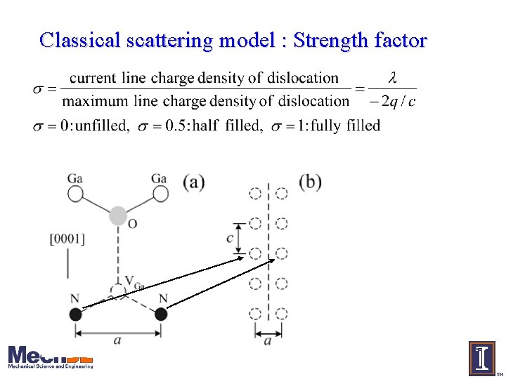
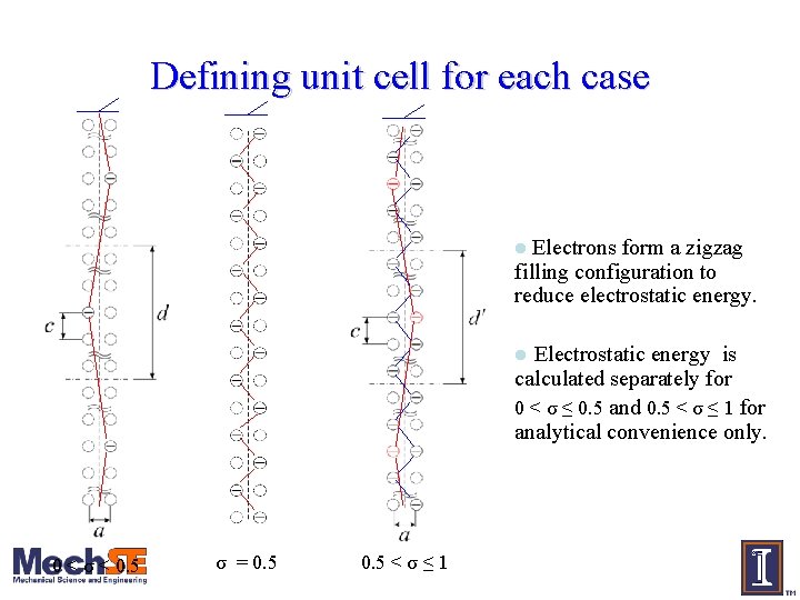
Classical scattering model: strength factor • Electron acceptors form array of two columns • Configuration is different from Ge dislocation • Determining strength factor a tricky electrostatics problem

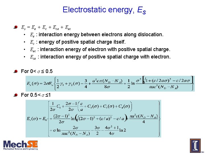
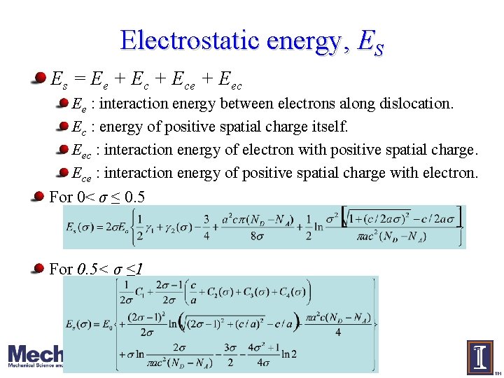
Electrostatic energy, ES Es = Ee + Ece + Eec • Ee : interaction energy between electrons along dislocation. • Ec : energy of positive spatial charge itself. • Eec : interaction energy of electron with positive spatial charge. • Ece : interaction energy of positive spatial charge with electron. For 0< σ ≤ 0. 5 For 0. 5< σ ≤ 1

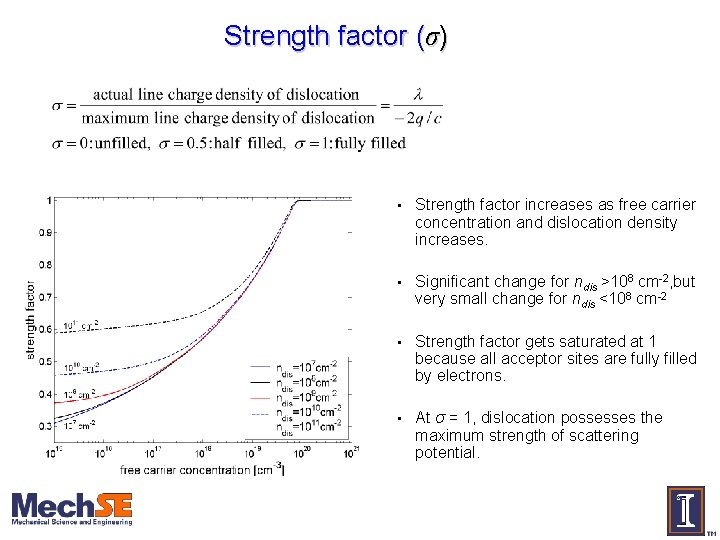
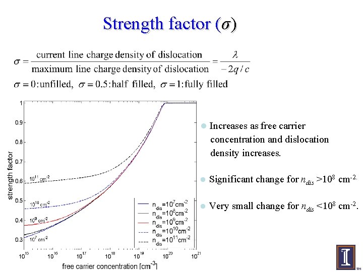
Strength factor (σ) • Strength factor increases as free carrier concentration and dislocation density increases. • Significant change for ndis >108 cm-2, but very small change for ndis <108 cm-2 • Strength factor gets saturated at 1 because all acceptor sites are fully filled by electrons. • At σ = 1, dislocation possesses the maximum strength of scattering potential.

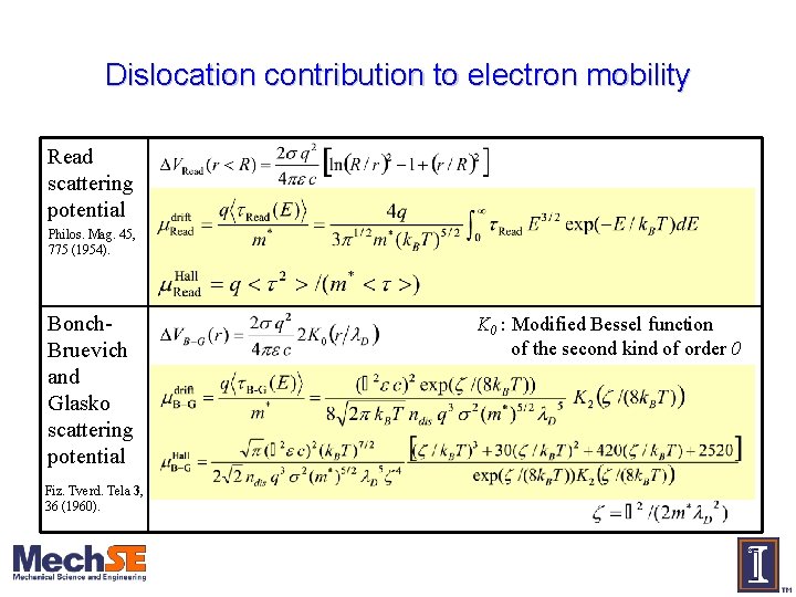
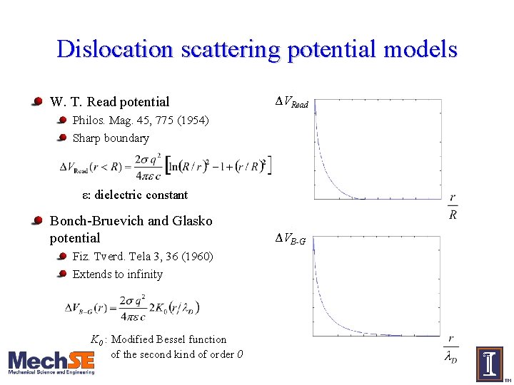
Dislocation contribution to electron mobility Read scattering potential Philos. Mag. 45, 775 (1954). Bonch. Bruevich and Glasko scattering potential Fiz. Tverd. Tela 3, 36 (1960). K 0 : Modified Bessel function of the second kind of order 0

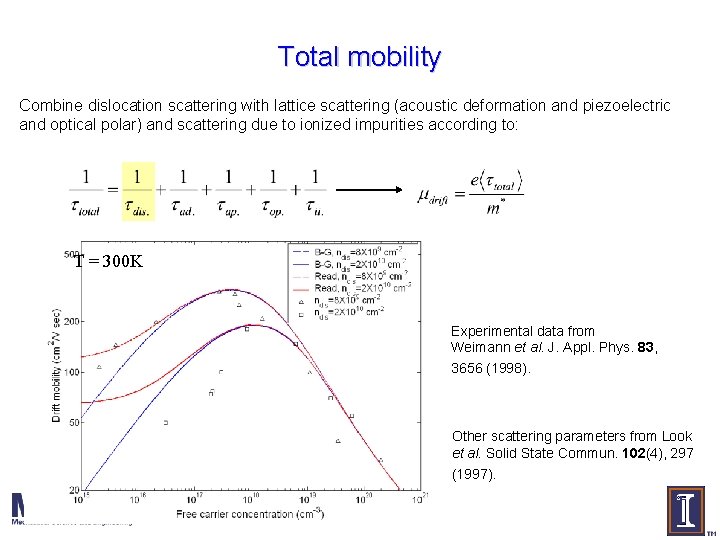
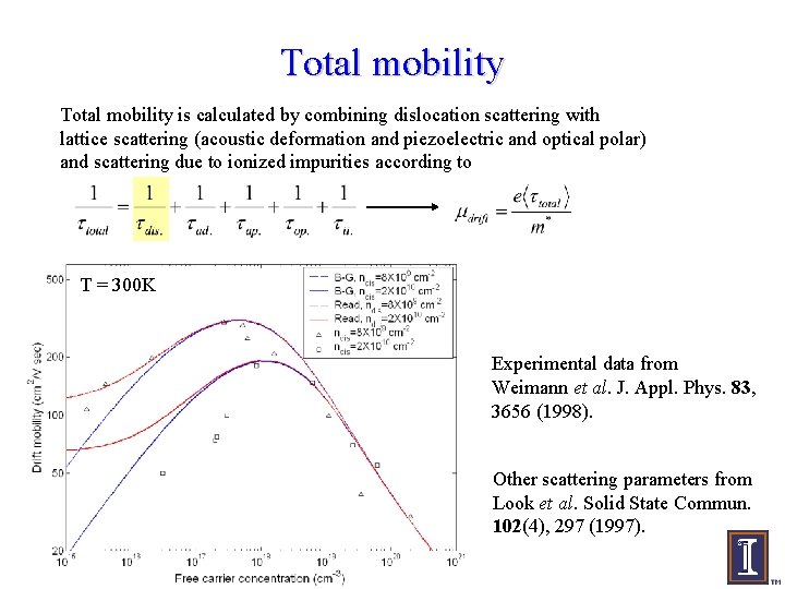
Total mobility Combine dislocation scattering with lattice scattering (acoustic deformation and piezoelectric and optical polar) and scattering due to ionized impurities according to: T = 300 K Experimental data from Weimann et al. J. Appl. Phys. 83, 3656 (1998). Other scattering parameters from Look et al. Solid State Commun. 102(4), 297 (1997).

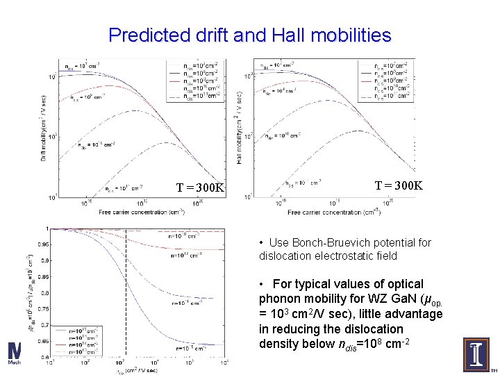
Predicted drift and Hall mobilities T = 300 K • Use Bonch-Bruevich potential for dislocation electrostatic field • For typical values of optical phonon mobility for WZ Ga. N (μop. = 103 cm 2/V sec), little advantage in reducing the dislocation density below ndis=108 cm-2

Summary and conclusions Dislocation effect on photoluminescence: Novel computational method to predict dislocation effect on optical properties Transition energies to dislocation-localized monopole state corresponds to YL, GL, and BL: 1. 9~3. 0 e. V Both calculated IBE and experimental data decrease (and broaden) as dislocation density increases for ndis >107 cm-2 Ga. N becomes dislocation-sensitive if insufficient carriers are provided Model explains significant difference between Ga. N and Ga. As Dislocation effect on electron mobility: Based on same physics at atomic scale, compute electron mobility using a classical scattering model Possible (depending on choice of electrostatic potential models for the dislocation core) to derive closed form analytical solution for dislocation effect on mobility Results in good agreement with experiments One implication: dislocation scattering not a significant factor below ndis=107 cm-2 You, Lu, and Johnson, J. Appl. Phys. 99, 033706 (2006) You and Johnson, J. Appl. Phys. 101, 023516 (2007) You and Johnson, Phys. Rev. B 76, 115336 (2007) also: htj@uiuc. edu

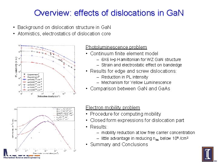
Overview: effects of dislocations in Ga. N • Background on dislocation structure in Ga. N • Atomistics, electrostatics of dislocation core Photoluminescence problem • Continuum finite element model – 6 X 6 k • p Hamiltonian for WZ Ga. N structure – Strain and electrostatic effect on bandedge • Results for edge and screw dislocations: – Reduction in PL intensity – Mechanism for Yellow Luminescence • Comparison between Ga. N and Ga. As Electron mobility problem • Procedure for computing mobility • Closed form expressions for dislocation part • Results: – mobility reduction at low free carrier concentration – little advantage in reducing ndis below 108 /cm 2 • Summary and Conclusions

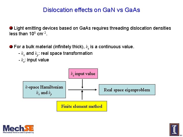
Dislocation effects on Ga. N vs Ga. As Light emitting devices based on Ga. As requires threading dislocation densities less than 106 cm-2. For a bulk material (infinitely thick), kz is a continuous value. - kx and ky: real space transformation - kz: input value kz input value k-space Hamiltonian kx and ky Finite element method Real space eigenproblem

Band structures Ga. As Ga. N

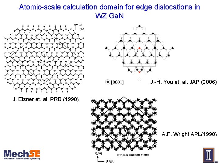
Atomic-scale calculation domain for edge dislocations in WZ Ga. N J. -H. You et. al. JAP (2006) J. Elsner et. al. PRB (1998) A. F. Wright APL(1998)

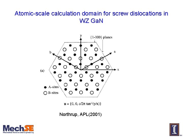
Atomic-scale calculation domain for screw dislocations in WZ Ga. N Northrup, APL(2001)

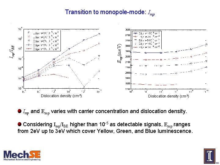
Imp/IBE Emp(me. V) Transition to monopole-mode: Imp Dislocation density (cm-2) Imp and Emp varies with carrier concentration and dislocation density. Considering Imp/IBE higher than 10 -5 as detectable signals, Emp ranges from 2 e. V up to 3 e. V which cover Yellow, Green, and Blue luminescence.

Calculation of filling fraction, f W. T. Read, Jr. , Philos. Mag. 45, 775 (1954) for Ge dislocation. Total increase of free energy of dislocation per electron Total increase of free energy of dislocation per acceptor site ES: electrostatic energy EF: Fermi level ET: dislocation level TS : entropy energy Minimizing f. F(f) w. r. t f Read derived Es(f) for dislocation in zincblende Ge lying on (111) which contains one acceptor per cell length forming a straight line of acceptors Need calculate Es(f) for WZ Ga. N dislocation along [0001]. [111] Ge dislocation

Classical scattering model : Strength factor

Electrostatic energy, ES Es = Ee + Ece + Eec Ee : interaction energy between electrons along dislocation. Ec : energy of positive spatial charge itself. Eec : interaction energy of electron with positive spatial charge. Ece : interaction energy of positive spatial charge with electron. For 0< σ ≤ 0. 5 For 0. 5< σ ≤ 1

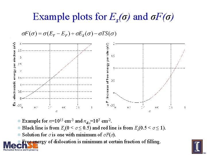
Strength factor (σ) l Increases as free carrier concentration and dislocation density increases. l Significant change for ndis >108 cm-2. l Very small change for ndis <108 cm-2.

Total mobility is calculated by combining dislocation scattering with lattice scattering (acoustic deformation and piezoelectric and optical polar) and scattering due to ionized impurities according to T = 300 K Experimental data from Weimann et al. J. Appl. Phys. 83, 3656 (1998). Other scattering parameters from Look et al. Solid State Commun. 102(4), 297 (1997).

Summary and Conclusion First-principle quantum mechanical calculation validates the charge distribution along the core of VGa-ON threading edge dislocation. Two N atoms near VGa act as electron acceptors and becomes up to -2 q/cell length charged scattering center. Strength factor was calculated Closed-form solutions of drift and Hall mobility were obtained. Calculated drift mobility fits reasonably well with experimental data. Expected drift and Hall mobility were shown. Very little advantage to reduce the density of dislocation below ndis=108 cm-2 for electron transport of WZ Ga. N.

Undoped N-doped with 6 Si atoms

Defining unit cell for each case Electrons form a zigzag filling configuration to reduce electrostatic energy. l Electrostatic energy is calculated separately for 0 < σ ≤ 0. 5 and 0. 5 < σ ≤ 1 for analytical convenience only. l 0 < σ < 0. 5 σ = 0. 5 < σ ≤ 1

Example plots for Es(σ) and σF(σ) Example for n=1015 cm-3 and ndis=107 cm-2. l Black line is from Es(0 < σ ≤ 0. 5) and red line is from Es(0. 5 < σ ≤ 1). l Solution for σ is one with minimum of σF(σ). l Free energy of dislocation is minimum at certain fraction of filling. l

Dislocation scattering potential models W. T. Read potential ΔVRead Philos. Mag. 45, 775 (1954) Sharp boundary ε: dielectric constant Bonch-Bruevich and Glasko potential Fiz. Tverd. Tela 3, 36 (1960) Extends to infinity K 0 : Modified Bessel function of the second kind of order 0 ΔVB-G

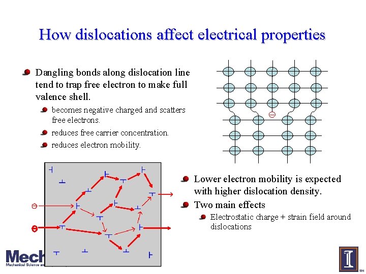
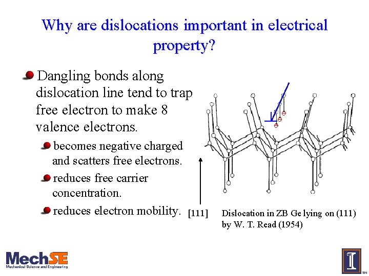
How dislocations affect electrical properties Dangling bonds along dislocation line tend to trap free electron to make full valence shell. becomes negative charged and scatters free electrons. reduces free carrier concentration. reduces electron mobility. Lower electron mobility is expected with higher dislocation density. Two main effects Electrostatic charge + strain field around dislocations

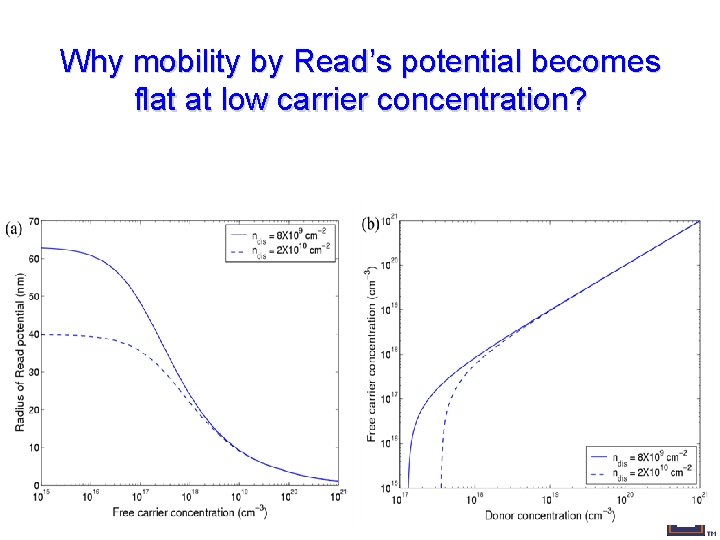
Why mobility by Read’s potential becomes flat at low carrier concentration?

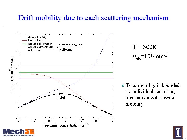
Drift mobility due to each scattering mechanism electron-phonon scattering Total T = 300 K ndis=1010 cm-2 o Total mobility is bounded by individual scattering mechanism with lowest mobility.

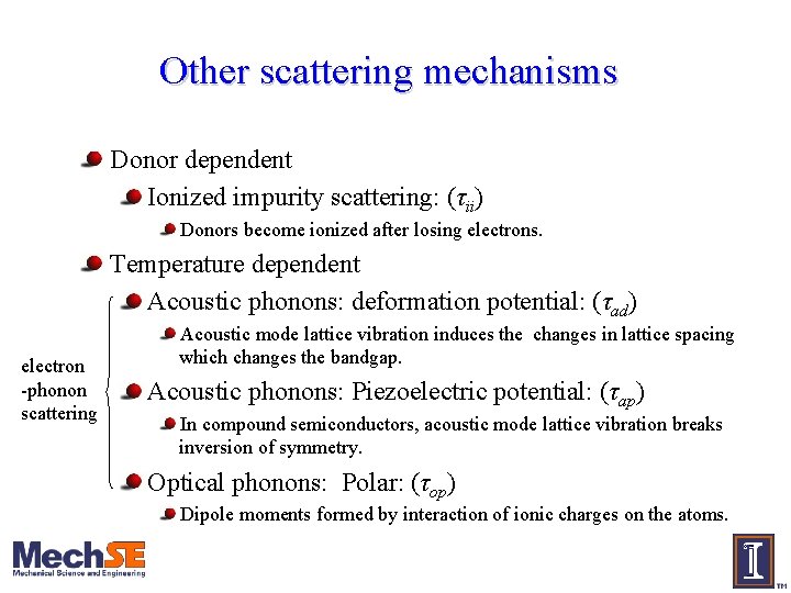
Other scattering mechanisms Donor dependent Ionized impurity scattering: (τii) Donors become ionized after losing electrons. Temperature dependent Acoustic phonons: deformation potential: (τad) electron -phonon scattering Acoustic mode lattice vibration induces the changes in lattice spacing which changes the bandgap. Acoustic phonons: Piezoelectric potential: (τap) In compound semiconductors, acoustic mode lattice vibration breaks inversion of symmetry. Optical phonons: Polar: (τop) Dipole moments formed by interaction of ionic charges on the atoms.

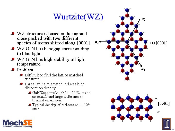
Wurtzite(WZ) Ga. N WZ structure is based on hexagonal close packed with two different species of atoms shifted along [0001]. a 3 WZ Ga. N has bandgap corresponding to blue light. WZ Ga. N has high stability at high temperature. Problem a 2 [0001] a 1 Difficult to find the lattice matched substrate. Large lattice mismatch induces high dislocation density. Ga. N/Sapphire(Al 2 O 3) : ~15 % lattice mismatch and large difference in thermal expansion. Typical density of dislocation : ~1010 cm-2 [0001] c

Why are dislocations important in electrical property? Dangling bonds along dislocation line tend to trap free electron to make 8 valence electrons. becomes negative charged and scatters free electrons. reduces free carrier concentration. reduces electron mobility. [111] Dislocation in ZB Ge lying on (111) by W. T. Read (1954)