Modeling and Design for Large Scale Heterogeneous Integration

- Slides: 59

Modeling and Design for Large Scale Heterogeneous Integration Neil Goldsman Dept. of Electrical and Computer Engineering, UMCP Collaborators: B. Jacob, A. Akturk, Z. Dilli, T. Chitnis, M. Khbeis and G. Metze

Modeling and Design for Large Scale Heterogeneous Integration Major Goal: Design, model and fabricate high performance circuits and systems using optimized devices, circuits, as well as 3 D and wafer-level integration.

Outline • Conventional Multi-Chip PC Board Integration § Summary and Limitations • Solutions • Research Tasks for Achieving Solutions § Device and Mixed Modeling § § Interconnect Modeling Circuit Prototyping Interconnect Prototyping and Characterization Passive components achievable with 3 D fabrication • Summary for Achieving High Performance 3 D Integrated System

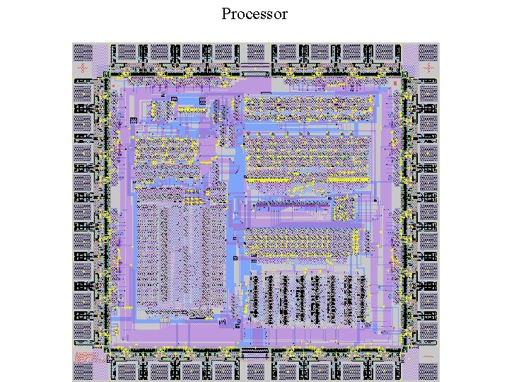
Processor

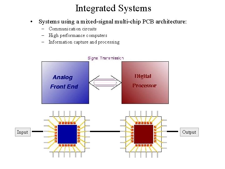
Integrated Systems • Systems using a mixed-signal multi-chip PCB architecture: – Communication circuits – High performance computers – Information capture and processing Input Output

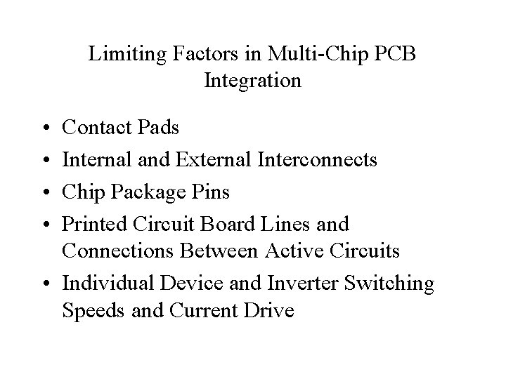
Limiting Factors in Multi-Chip PCB Integration • • Contact Pads Internal and External Interconnects Chip Package Pins Printed Circuit Board Lines and Connections Between Active Circuits • Individual Device and Inverter Switching Speeds and Current Drive

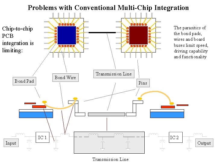
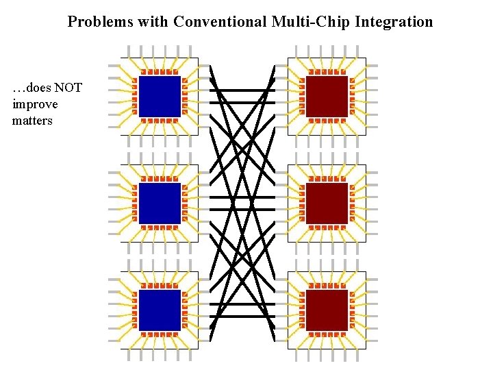
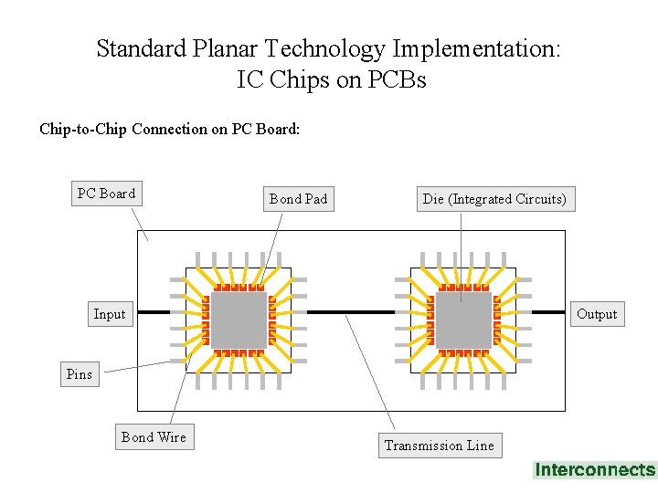
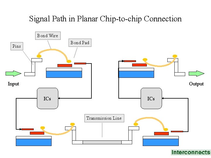
Problems with Conventional Multi-Chip Integration The parasitics of the bond pads, wires and board buses limit speed, driving capability and functionality Chip-to-chip PCB integration is limiting: Bond Wire Bond Pad Transmission Line Pins IC 1 IC 2 Input Output Transmission Line

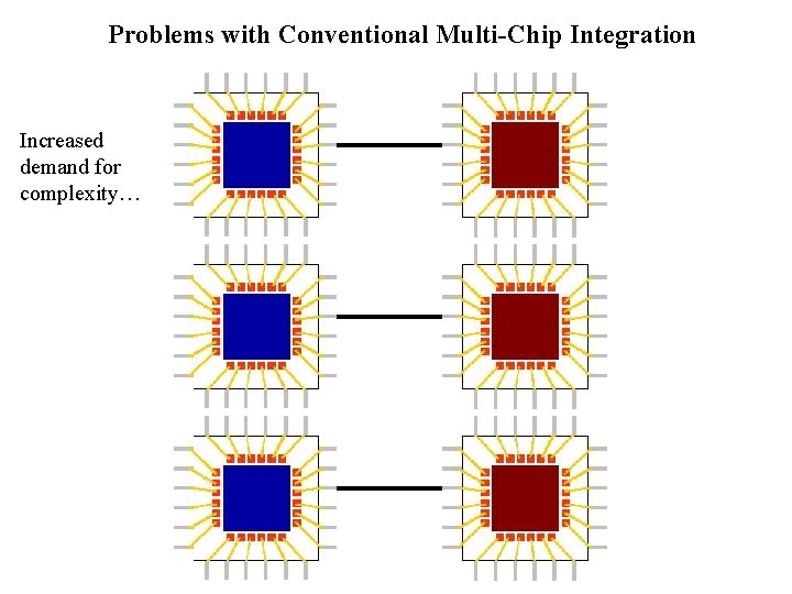
Problems with Conventional Multi-Chip Integration Increased demand for complexity…

Problems with Conventional Multi-Chip Integration …does NOT improve matters

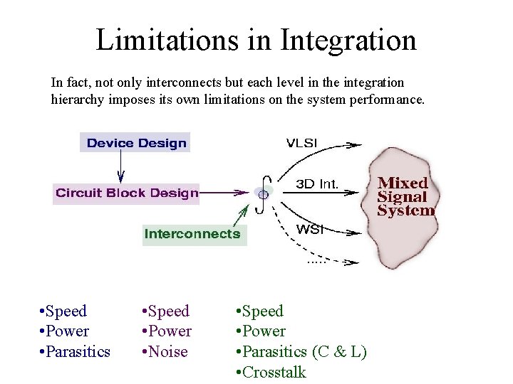
Limitations in Integration In fact, not only interconnects but each level in the integration hierarchy imposes its own limitations on the system performance. • Speed • Power • Parasitics • Speed • Power • Noise • Speed • Power • Parasitics (C & L) • Crosstalk

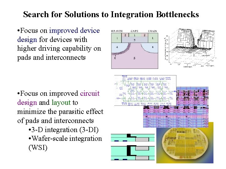
Search for Solutions to Integration Bottlenecks • Focus on improved device design for devices with higher driving capability on pads and interconnects • Focus on improved circuit design and layout to minimize the parasitic effect of pads and interconnects • 3 -D integration (3 -DI) • Wafer-scale integration (WSI)

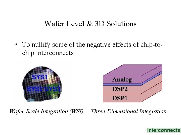
Wafer Level & 3 D Solutions • To nullify some of the negative effects of chip-tochip interconnects Wafer-Scale Integration (WSI) Three-Dimensional Integration

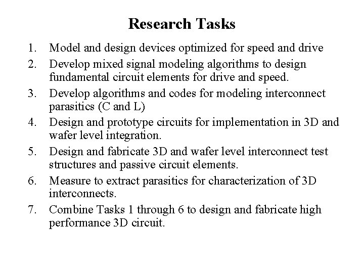
Research Tasks 1. Model and design devices optimized for speed and drive 2. Develop mixed signal modeling algorithms to design fundamental circuit elements for drive and speed. 3. Develop algorithms and codes for modeling interconnect parasitics (C and L) 4. Design and prototype circuits for implementation in 3 D and wafer level integration. 5. Design and fabricate 3 D and wafer level interconnect test structures and passive circuit elements. 6. Measure to extract parasitics for characterization of 3 D interconnects. 7. Combine Tasks 1 through 6 to design and fabricate high performance 3 D circuit.

Task 1. Model and Design devices optimized for speed and drive

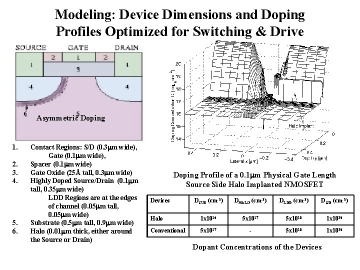
Modeling: Device Dimensions and Doping Profiles Optimized for Switching & Drive Asymmetric Doping 1. 2. 3. 4. 5. 6. Contact Regions: S/D (0. 3 m wide), Gate (0. 1 m wide), Spacer (0. 1 m wide) Gate Oxide (25Å tall, 0. 3 m wide) Highly Doped Source/Drain (0. 1 m tall, 0. 35 m wide) LDD Regions are at the edges of channel (0. 05 m tall, 0. 05 m wide) Substrate (0. 5 m tall, 0. 9 m wide) Halo (0. 01 m thick, either around the Source or Drain) Doping Profile of a 0. 1 m Physical Gate Length Source Side Halo Implanted NMOSFET Devices DSUB (cm-3) DHALO (cm-3) DLDD (cm-3) DS/D (cm-3) Halo 1 x 10¹⁶ 5 x 10¹⁷ 5 x 10¹⁸ 1 x 10²⁰ Conventional 5 x 10¹⁷ - 5 x 10¹⁸ 1 x 10²⁰ Dopant Concentrations of the Devices

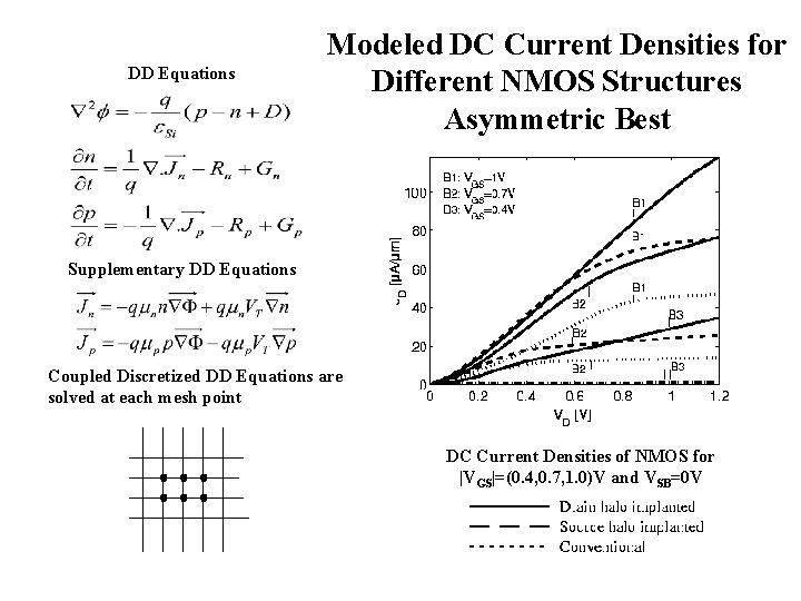
DD Equations Modeled DC Current Densities for Different NMOS Structures Asymmetric Best Supplementary DD Equations Coupled Discretized DD Equations are solved at each mesh point DC Current Densities of NMOS for |VGS|=(0. 4, 0. 7, 1. 0)V and VSB=0 V

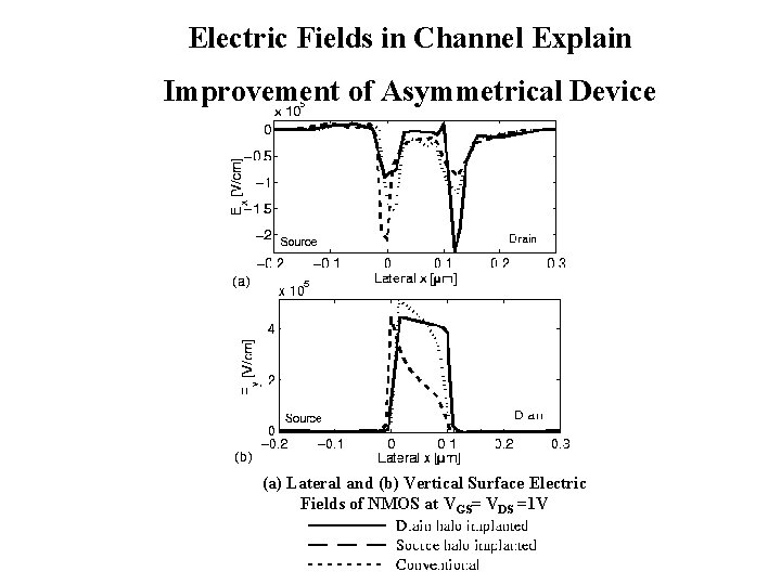
Electric Fields in Channel Explain Improvement of Asymmetrical Device (a) Lateral and (b) Vertical Surface Electric Fields of NMOS at VGS= VDS =1 V

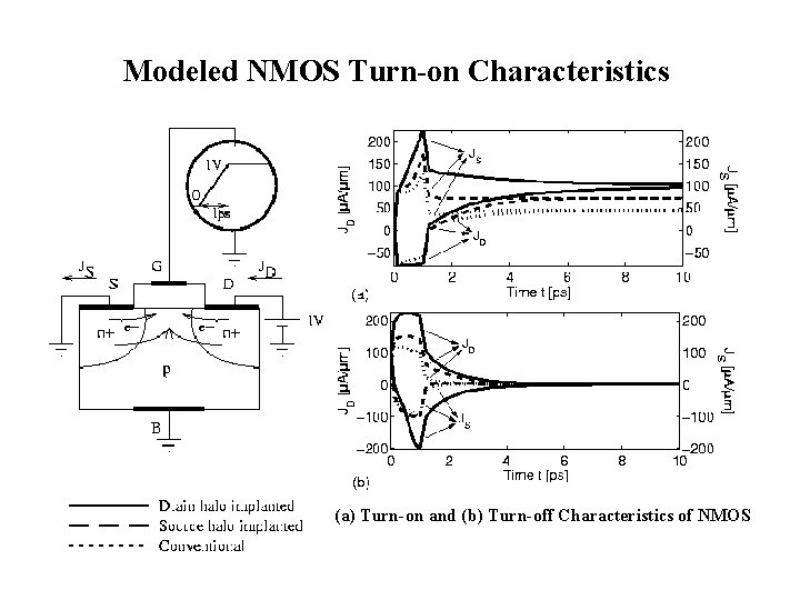
Modeled NMOS Turn-on Characteristics (a) Turn-on and (b) Turn-off Characteristics of NMOS

Task 2. Develop mixed signal modeling algorithms to design fundamental circuit elements for drive and speed.

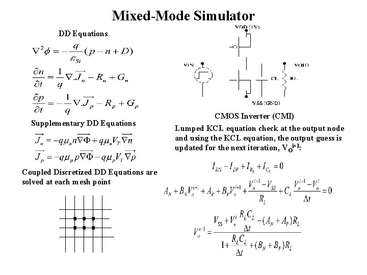
Mixed-Mode Simulator DD Equations Supplementary DD Equations Coupled Discretized DD Equations are solved at each mesh point CMOS Inverter (CMI) Lumped KCL equation check at the output node and using the KCL equation, the output guess is updated for the next iteration, VOi+1:

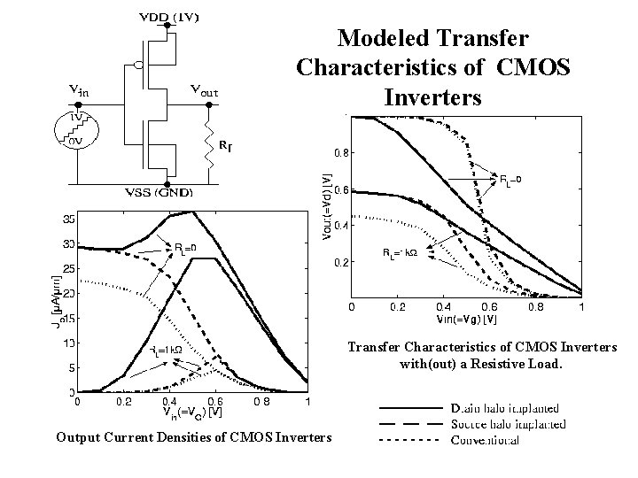
Modeled Transfer Characteristics of CMOS Inverters with(out) a Resistive Load. Output Current Densities of CMOS Inverters

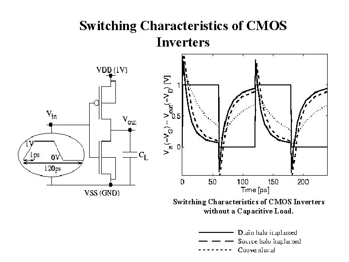
Switching Characteristics of CMOS Inverters without a Capacitive Load.

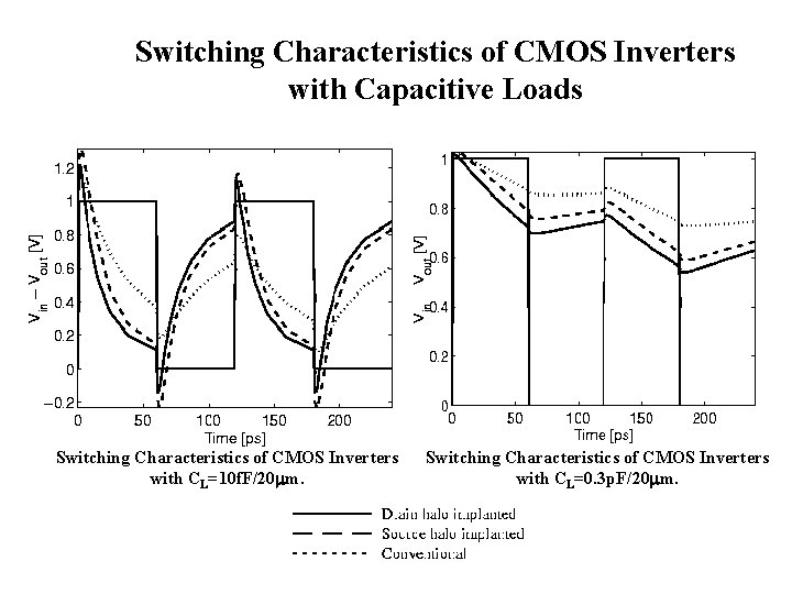
Switching Characteristics of CMOS Inverters with Capacitive Loads Switching Characteristics of CMOS Inverters with CL=10 f. F/20 m. Switching Characteristics of CMOS Inverters with CL=0. 3 p. F/20 m.

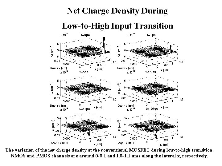
Net Charge Density During Low-to-High Input Transition The variation of the net charge density at the conventional MOSFET during low-to-high transition. NMOS and PMOS channels are around 0 -0. 1 and 1. 0 -1. 1 μms along the lateral x, respectively.

Task 3: Calculation of the Induced Voltage on Floating Metals via Capacitive Effects

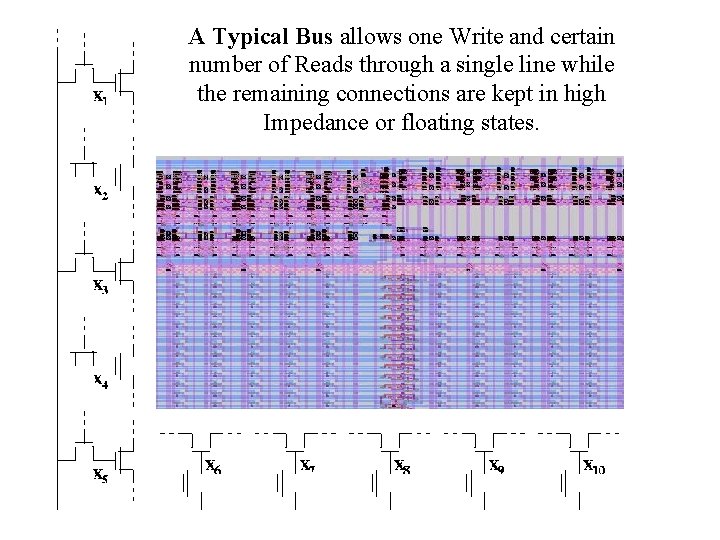
A Typical Bus allows one Write and certain number of Reads through a single line while the remaining connections are kept in high Impedance or floating states.

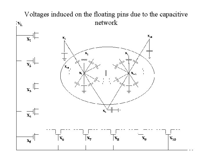
Voltages induced on the floating pins due to the capacitive network

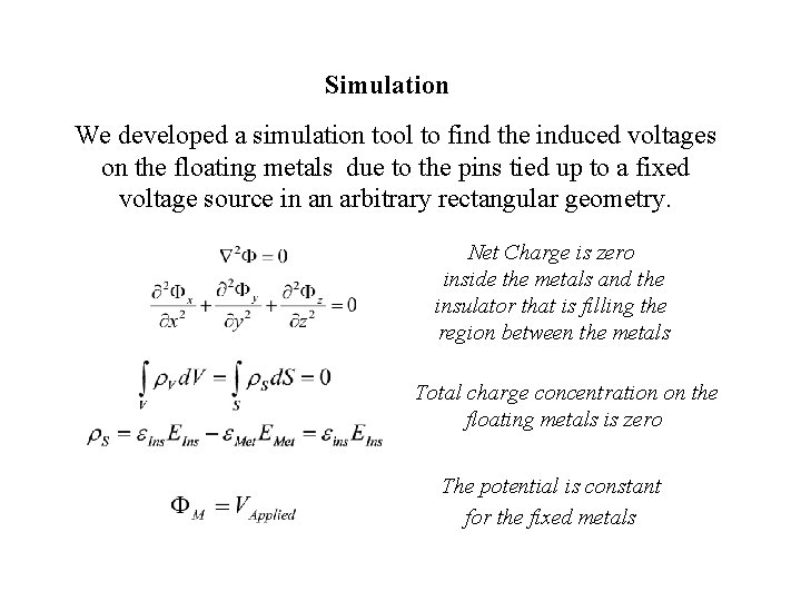
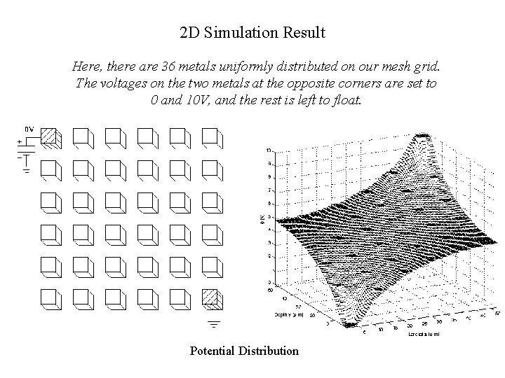
Simulation We developed a simulation tool to find the induced voltages on the floating metals due to the pins tied up to a fixed voltage source in an arbitrary rectangular geometry. Net Charge is zero inside the metals and the insulator that is filling the region between the metals Total charge concentration on the floating metals is zero The potential is constant for the fixed metals

2 D Simulation Result Here, there are 36 metals uniformly distributed on our mesh grid. The voltages on the two metals at the opposite corners are set to 0 and 10 V, and the rest is left to float. Potential Distribution

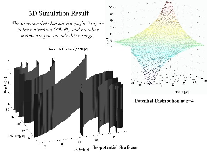
3 D Simulation Result The previous distribution is kept for 3 layers in the z direction (3 rd-5 th), and no other metals are put outside this z range Potential Distribution at z=4 Isopotential Surfaces

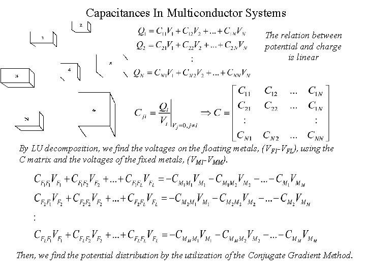
Capacitances In Multiconductor Systems The relation between potential and charge is linear By LU decomposition, we find the voltages on the floating metals, (VF 1 -VFL), using the C matrix and the voltages of the fixed metals, (VM 1 -VMM). Then, we find the potential distribution by the utilization of the Conjugate Gradient Method.

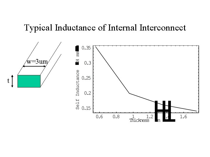
Typical Inductance of Internal Interconnect w=3 um t

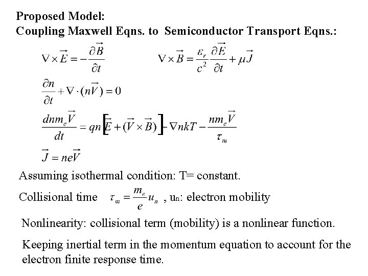
Proposed Model: Coupling Maxwell Eqns. to Semiconductor Transport Eqns. : Assuming isothermal condition: T= constant. Collisional time , un: electron mobility Nonlinearity: collisional term (mobility) is a nonlinear function. Keeping inertial term in the momentum equation to account for the electron finite response time.

Task 4: Design and prototype circuits for implementation in 3 D and wafer level integration.

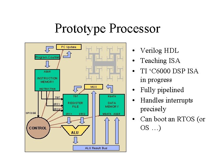
Prototype Processor PC Update Program Counter ADDR INSTRUCTION MEMORY MUX INSTRUCTION TGT RDATA REGISTER FILE DATA MEMORY TGT SRC 1 SRC 2 OPCODE SRC 1 SRC 2 WDATA ADDR CONTROL ALU Result Bus • Verilog HDL • Teaching ISA • TI ‘C 6000 DSP ISA in progress • Fully pipelined • Handles interrupts precisely • Can boot an RTOS (or OS …)

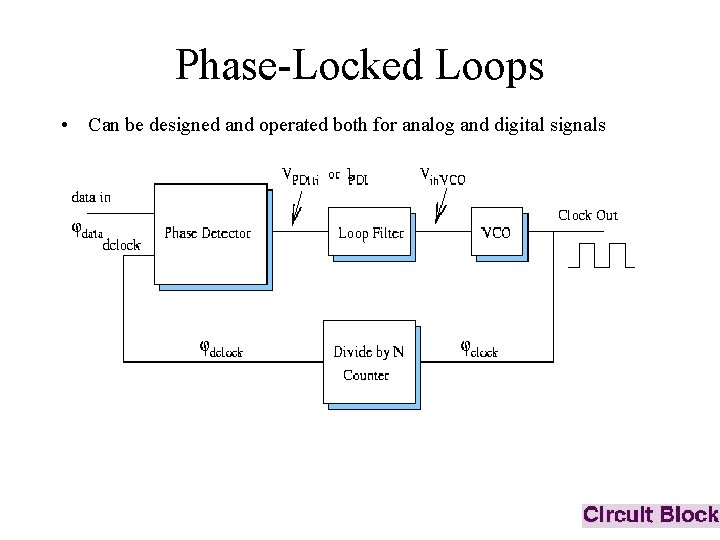
Phase-Locked Loops • Can be designed and operated both for analog and digital signals

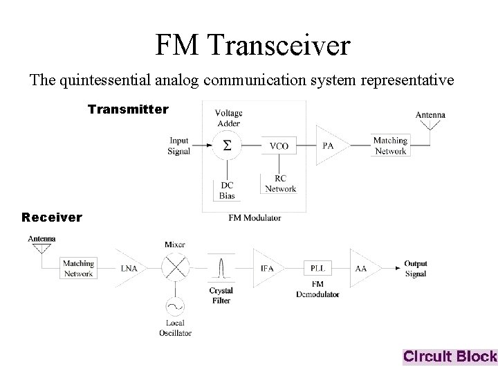
FM Transceiver The quintessential analog communication system representative Transmitter Receiver

Task 5: Design and fabricate 3 D and wafer level interconnect test structures and passive circuit elements. On-Chip Inductors and Transformers: Surface versus 3 D

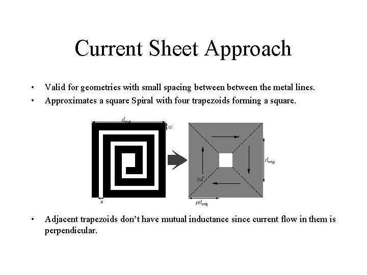
Current Sheet Approach • • Valid for geometries with small spacing between the metal lines. Approximates a square Spiral with four trapezoids forming a square. • Adjacent trapezoids don’t have mutual inductance since current flow in them is perpendicular.

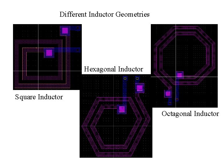
Different Inductor Geometries Hexagonal Inductor Square Inductor Octagonal Inductor

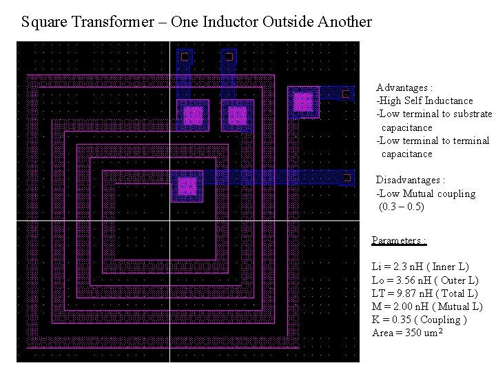
Square Transformer – One Inductor Outside Another Advantages : -High Self Inductance -Low terminal to substrate capacitance -Low terminal to terminal capacitance Disadvantages : -Low Mutual coupling (0. 3 – 0. 5) Parameters : Li = 2. 3 n. H ( Inner L) Lo = 3. 56 n. H ( Outer L) LT = 9. 87 n. H ( Total L) M = 2. 00 n. H ( Mutual L) K = 0. 35 ( Coupling ) Area = 350 um 2

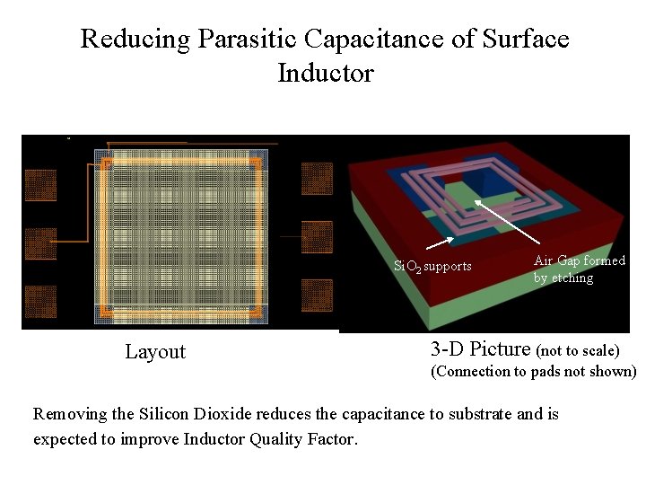
Reducing Parasitic Capacitance of Surface Inductor Si. O 2 supports Layout Air Gap formed by etching 3 -D Picture (not to scale) (Connection to pads not shown) Removing the Silicon Dioxide reduces the capacitance to substrate and is expected to improve Inductor Quality Factor.

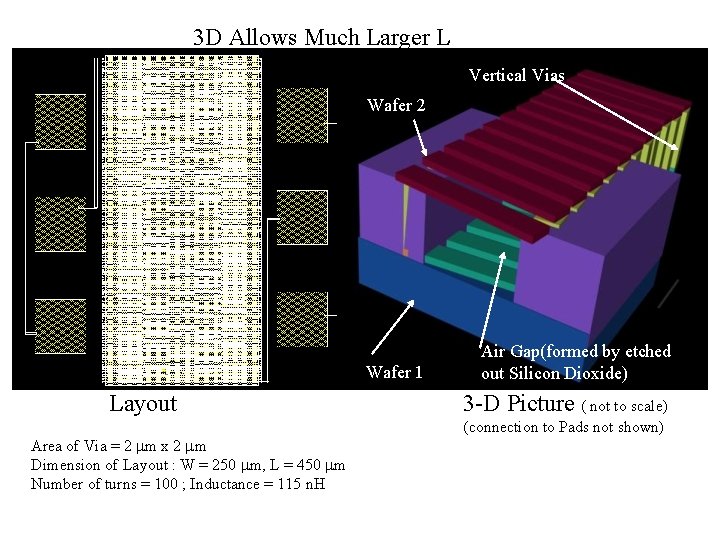
3 D Allows Much Larger L Vertical Vias Wafer 2 Wafer 1 Layout Area of Via = 2 m x 2 m Dimension of Layout : W = 250 m, L = 450 m Number of turns = 100 ; Inductance = 115 n. H Air Gap(formed by etched out Silicon Dioxide) 3 -D Picture ( not to scale) (connection to Pads not shown)

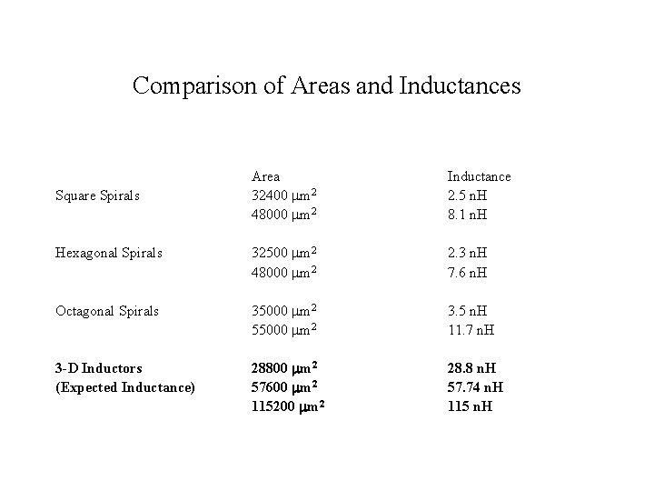
Comparison of Areas and Inductances Area 32400 m 2 48000 m 2 Inductance 2. 5 n. H 8. 1 n. H Hexagonal Spirals 32500 m 2 48000 m 2 2. 3 n. H 7. 6 n. H Octagonal Spirals 35000 m 2 55000 m 2 3. 5 n. H 11. 7 n. H 3 -D Inductors (Expected Inductance) 28800 m 2 57600 m 2 115200 m 2 28. 8 n. H 57. 74 n. H 115 n. H Square Spirals

Task 6: Measure to extract parasitics for characterization of 3 D interconnects. Preliminary analysis indicates pad, pin parasitics are significantly detrimental. Test structure layout complete; submission to Northrop Grumman immenant. (M. Khbeis, G. Metze)

Conclusion • Conventional Multi-Chip PC Board Integration § Summary and Limitations • Solutions • Research Tasks for Achieving Solutions § Device and Mixed Modeling § § Interconnect Modeling Circuit Prototyping Interconnect Prototyping and Characterization Passive components achievable with 3 D fabrication

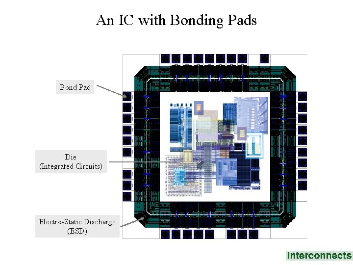
An IC with Bonding Pads Bond Pad Die (Integrated Circuits) Electro-Static Discharge (ESD)

Standard Planar Technology Implementation: IC Chips on PCBs Chip-to-Chip Connection on PC Board: PC Board Bond Pad Die (Integrated Circuits) Input Output Pins Bond Wire Transmission Line

Signal Path in Planar Chip-to-chip Connection Bond Wire Bond Pad Pins Input Output ICs Transmission Line

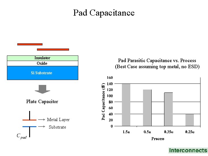
Pad Capacitance Metal Insulator Oxide Si Substrate Plate Capacitor Metal Layer Substrate Pad Parasitic Capacitance vs. Process (Best Case assuming top metal, no ESD)

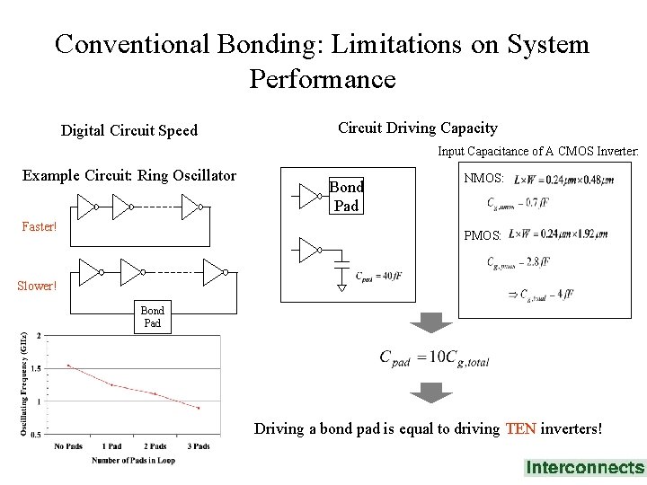
Conventional Bonding: Limitations on System Performance Digital Circuit Speed Circuit Driving Capacity Input Capacitance of A CMOS Inverter: Example Circuit: Ring Oscillator Faster! Bond Pad NMOS: PMOS: Slower! Bond Pad Driving a bond pad is equal to driving TEN inverters!

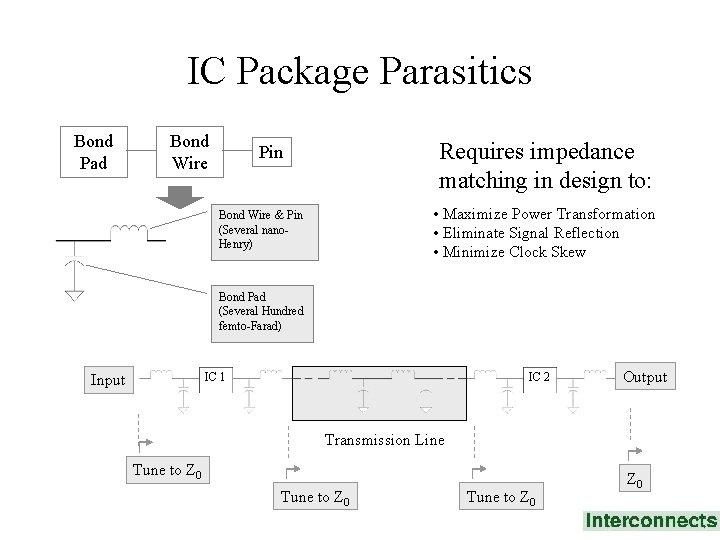
IC Package Parasitics Bond Pad Bond Wire Requires impedance matching in design to: Pin • Maximize Power Transformation • Eliminate Signal Reflection • Minimize Clock Skew Bond Wire & Pin (Several nano. Henry) Bond Pad (Several Hundred femto-Farad) IC 1 Input IC 2 Output Transmission Line Tune to Z 0

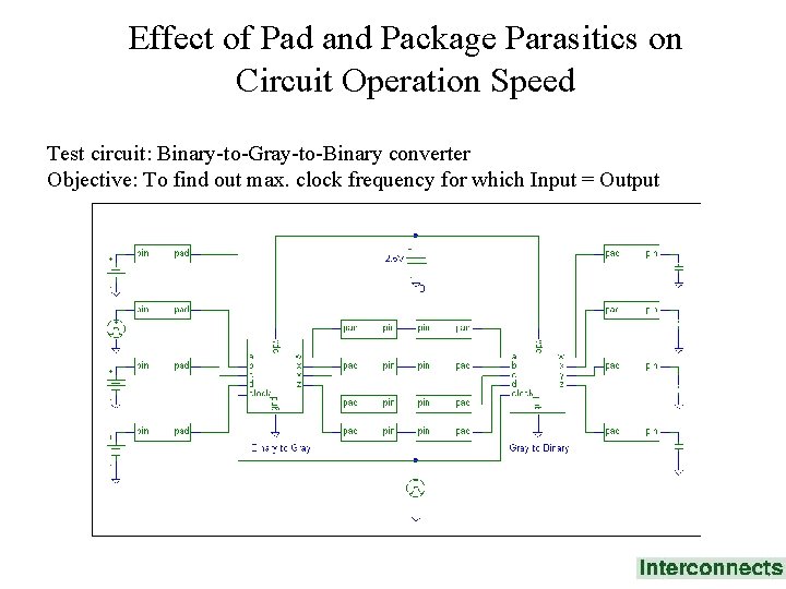
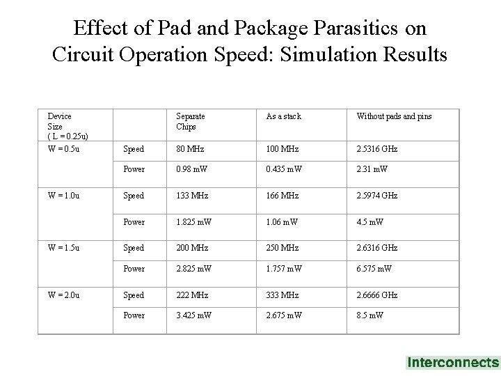
Effect of Pad and Package Parasitics on Circuit Operation Speed Test circuit: Binary-to-Gray-to-Binary converter Objective: To find out max. clock frequency for which Input = Output

Effect of Pad and Package Parasitics on Circuit Operation Speed: Simulation Results Device Size ( L = 0. 25 u) W = 0. 5 u W = 1. 0 u W = 1. 5 u W = 2. 0 u Separate Chips As a stack Without pads and pins Speed 80 MHz 100 MHz 2. 5316 GHz Power 0. 98 m. W 0. 435 m. W 2. 31 m. W Speed 133 MHz 166 MHz 2. 5974 GHz Power 1. 825 m. W 1. 06 m. W 4. 5 m. W Speed 200 MHz 250 MHz 2. 6316 GHz Power 2. 825 m. W 1. 757 m. W 6. 575 m. W Speed 222 MHz 333 MHz 2. 6666 GHz Power 3. 425 m. W 2. 675 m. W 8. 5 m. W

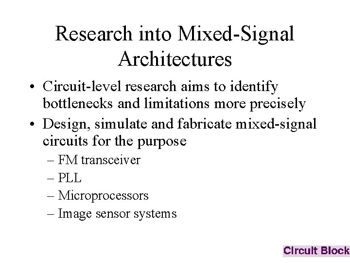
Research into Mixed-Signal Architectures • Circuit-level research aims to identify bottlenecks and limitations more precisely • Design, simulate and fabricate mixed-signal circuits for the purpose – FM transceiver – PLL – Microprocessors – Image sensor systems

Processor? Insert material from Dr. Jacob here?

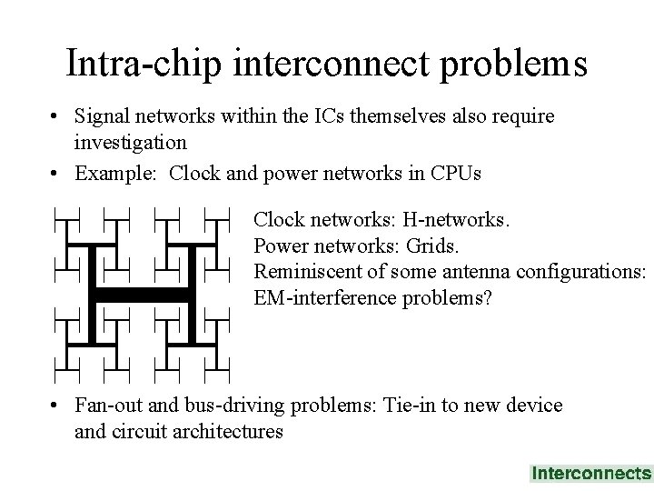
Intra-chip interconnect problems • Signal networks within the ICs themselves also require investigation • Example: Clock and power networks in CPUs Clock networks: H-networks. Power networks: Grids. Reminiscent of some antenna configurations: EM-interference problems? • Fan-out and bus-driving problems: Tie-in to new device and circuit architectures

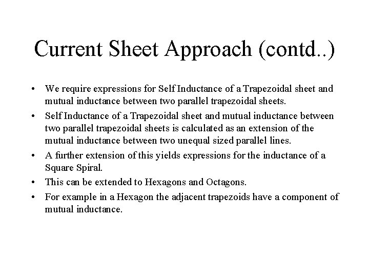
Current Sheet Approach (contd. . ) • We require expressions for Self Inductance of a Trapezoidal sheet and mutual inductance between two parallel trapezoidal sheets. • Self Inductance of a Trapezoidal sheet and mutual inductance between two parallel trapezoidal sheets is calculated as an extension of the mutual inductance between two unequal sized parallel lines. • A further extension of this yields expressions for the inductance of a Square Spiral. • This can be extended to Hexagons and Octagons. • For example in a Hexagon the adjacent trapezoids have a component of mutual inductance.

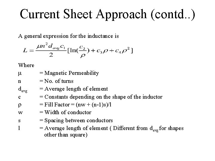
Current Sheet Approach (contd. . ) A general expression for the inductance is Where n davg c r w s l = Magnetic Permeability = No. of turns = Average length of element = Constants depending on the shape of the inductor = Fill Factor = (nw + (n-1)s)/l = Width of conductor = Spacing between conductors = Average length of element ( Different from davg for shapes other than square)