MLP Aware Heterogeneous Memory System Sujay Phadke Satish


- Slides: 36

MLP Aware Heterogeneous Memory System Sujay Phadke Satish Narayanasamy 16 th March, 2011 University of Michigan, Ann Arbor

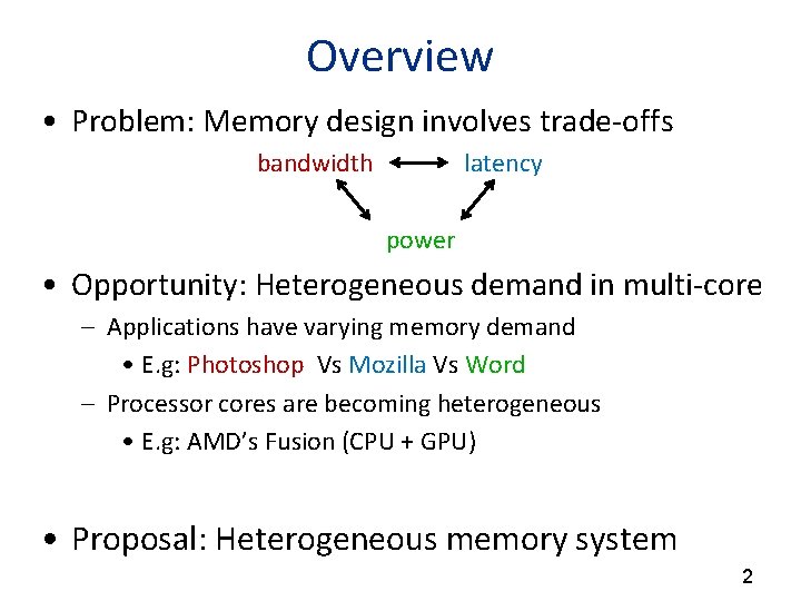
Overview • Problem: Memory design involves trade-offs bandwidth latency power • Opportunity: Heterogeneous demand in multi-core – Applications have varying memory demand • E. g: Photoshop Vs Mozilla Vs Word – Processor cores are becoming heterogeneous • E. g: AMD’s Fusion (CPU + GPU) • Proposal: Heterogeneous memory system 2

Outline • • • Motivation Memory Design Classifying Applications Using MLP Results Conclusions 3

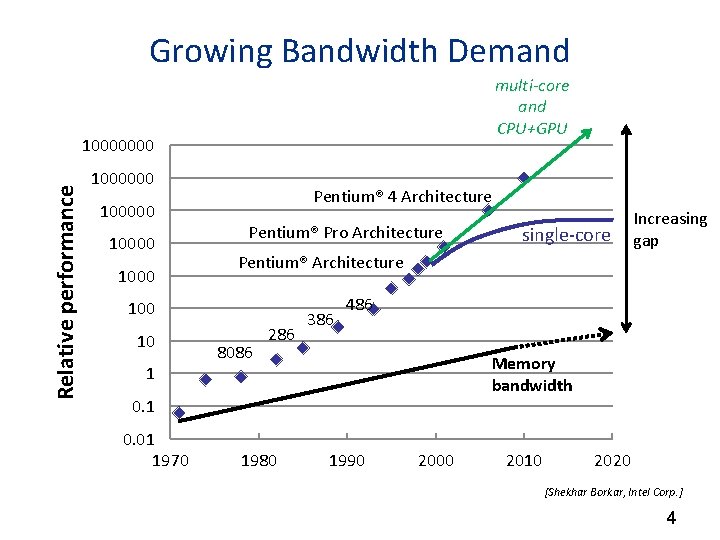
Growing Bandwidth Demand multi-core and CPU+GPU Relative performance 10000000 100000 1000 Pentium® 4 Architecture Pentium® Pro Architecture Pentium® Architecture 100 10 1 8086 286 386 486 Memory bandwidth 0. 1 0. 01 1970 single-core 1980 Increasing gap 1990 2000 2010 2020 [Shekhar Borkar, Intel Corp. ] 4

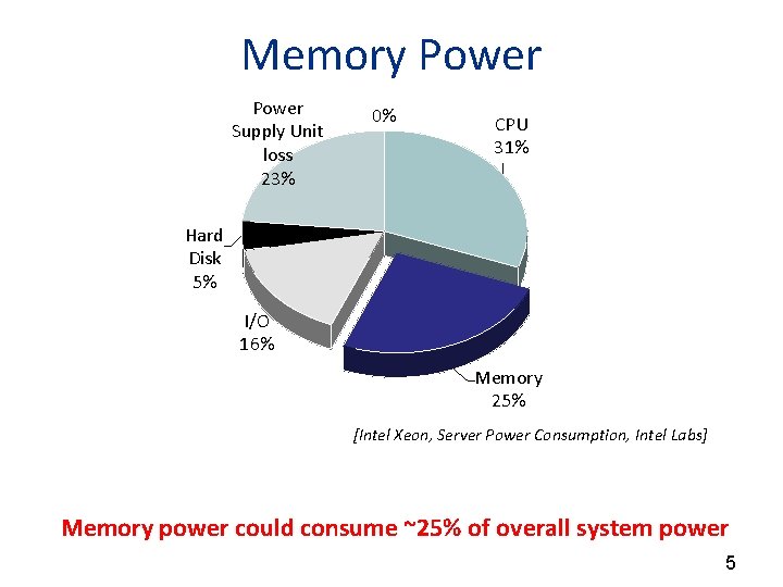
Memory Power Supply Unit loss 23% 0% CPU 31% Hard Disk 5% I/O 16% Memory 25% [Intel Xeon, Server Power Consumption, Intel Labs] Memory power could consume ~25% of overall system power 5

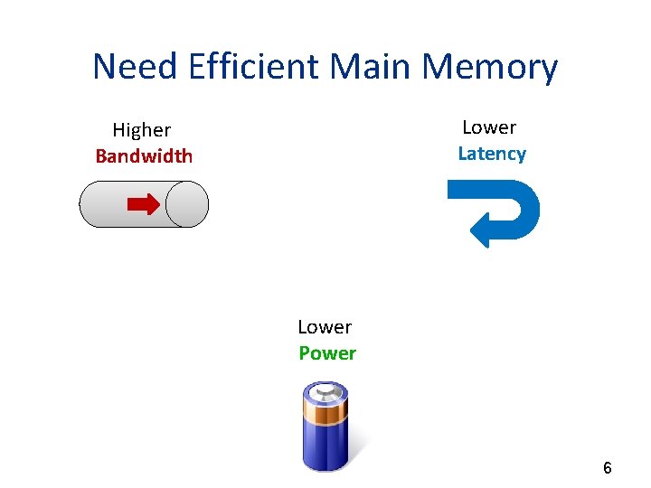
Need Efficient Main Memory Lower Latency Higher Bandwidth Lower Power 6

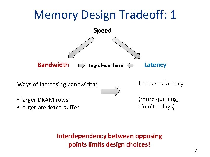
Memory Design Tradeoff: 1 Speed Bandwidth Tug-of-war here Latency Ways of increasing bandwidth: Increases latency • larger DRAM rows • larger pre-fetch buffer (more queuing, circuit delays) Interdependency between opposing points limits design choices! 7

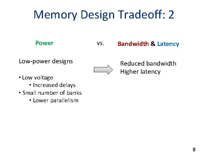
Memory Design Tradeoff: 2 Power Low-power designs • Low voltage vs. Bandwidth & Latency Reduced bandwidth Higher latency • Increased delays • Small number of banks • Lower parallelism 8

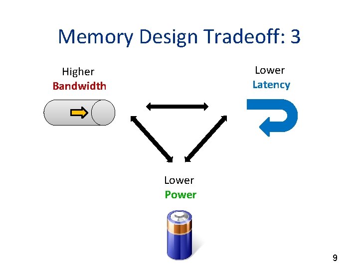
Memory Design Tradeoff: 3 Lower Latency Higher Bandwidth Lower Power 9

Opportunity: Heterogeneity in Multi-cores Applications that concurrently run on a multi-core system have varying memory demands Processor cores are heterogeneous 10

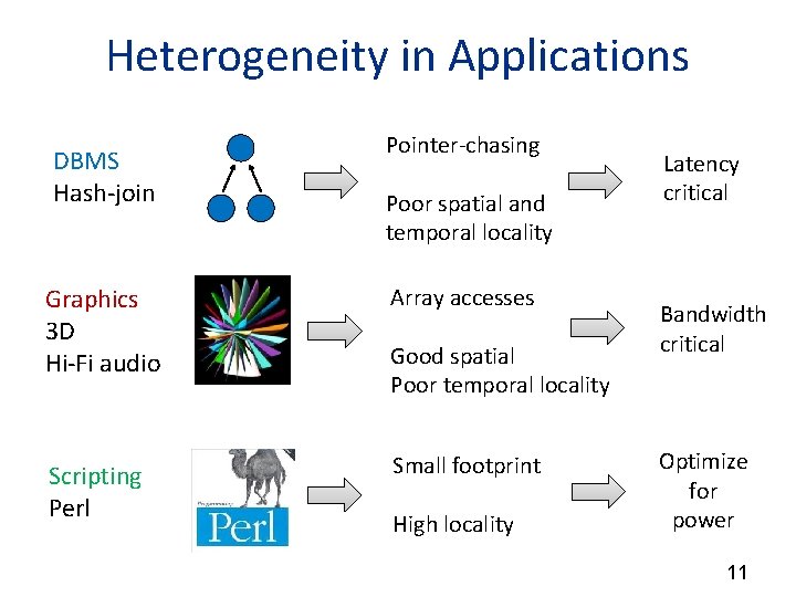
Heterogeneity in Applications DBMS Hash-join Pointer-chasing Poor spatial and temporal locality Graphics 3 D Hi-Fi audio Array accesses Scripting Perl Small footprint Good spatial Poor temporal locality High locality Latency critical Bandwidth critical Optimize for power 11

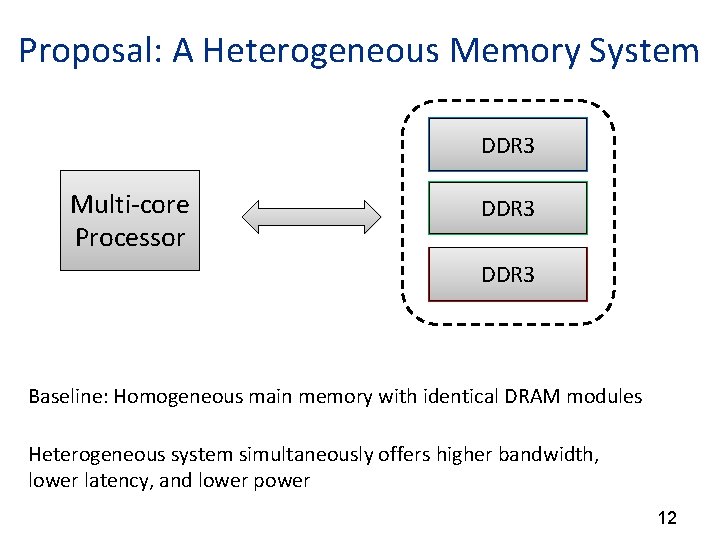
Proposal: A Heterogeneous Memory System Low. DDR 3 Latency Multi-core Processor Low DDR 3 Power High. DDR 3 Bandwidth Baseline: Homogeneous main memory with identical DRAM modules Heterogeneous system simultaneously offers higher bandwidth, lower latency, and lower power 12

Outline • • • Motivation Memory Design Classifying Applications Using MLP Results Conclusions 13

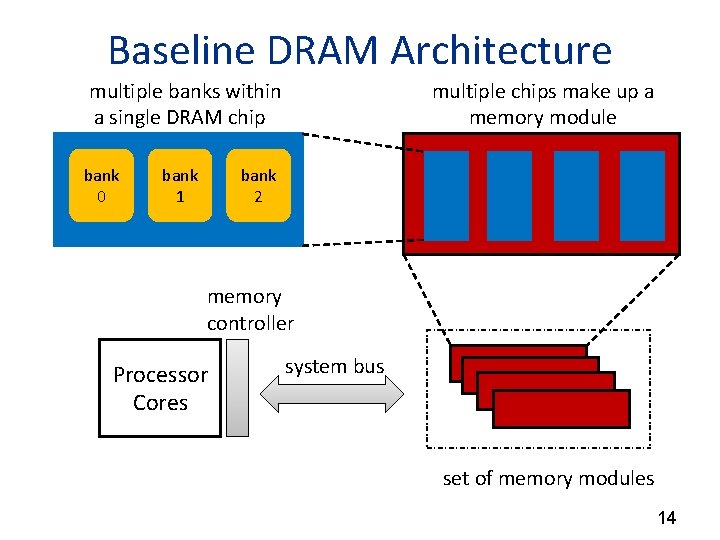
Baseline DRAM Architecture multiple banks within a single DRAM chip bank 0 bank 1 multiple chips make up a memory module bank 2 memory controller Processor Cores system bus set of memory modules 14

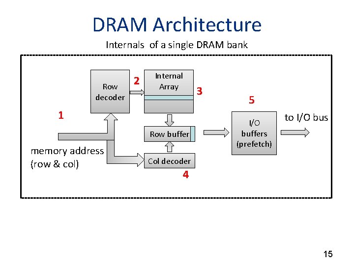
DRAM Architecture Internals of a single DRAM bank Row decoder 2 Internal Array 3 1 Row buffer memory address (row & col) 5 I/O buffers (prefetch) to I/O bus Col decoder 4 15

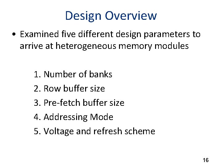
Design Overview • Examined five different design parameters to arrive at heterogeneous memory modules 1. Number of banks 2. Row buffer size 3. Pre-fetch buffer size 4. Addressing Mode 5. Voltage and refresh scheme 16

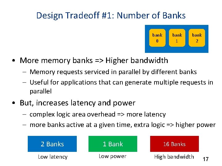
Design Tradeoff #1: Number of Banks bank 0 bank 1 bank 2 • More memory banks => Higher bandwidth – Memory requests serviced in parallel by different banks – Useful for applications that can generate multiple requests in parallel • But, increases latency and power – complex logic area overhead => more latency – more banks active at a given time, extra logic => higher power 2 Banks 1 Bank 16 Banks Low latency Low power High bandwidth 17

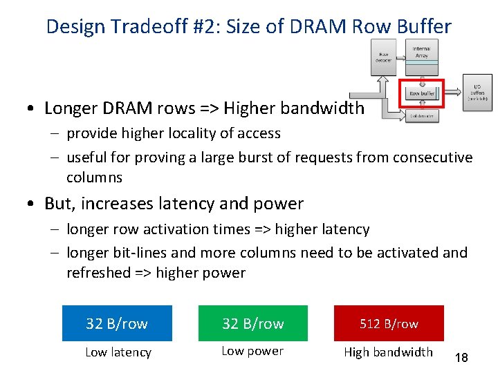
Design Tradeoff #2: Size of DRAM Row Buffer • Longer DRAM rows => Higher bandwidth – provide higher locality of access – useful for proving a large burst of requests from consecutive columns • But, increases latency and power – longer row activation times => higher latency – longer bit-lines and more columns need to be activated and refreshed => higher power 32 B/row 512 B/row Low latency Low power High bandwidth 18

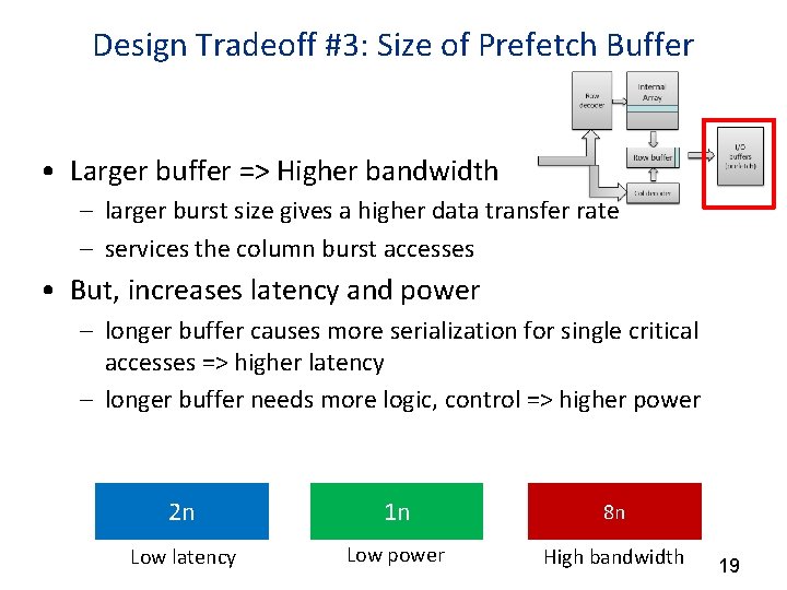
Design Tradeoff #3: Size of Prefetch Buffer • Larger buffer => Higher bandwidth – larger burst size gives a higher data transfer rate – services the column burst accesses • But, increases latency and power – longer buffer causes more serialization for single critical accesses => higher latency – longer buffer needs more logic, control => higher power 2 n 1 n 8 n Low latency Low power High bandwidth 19

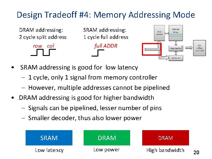
Design Tradeoff #4: Memory Addressing Mode DRAM addressing: 2 cycle split address SRAM addressing: 1 cycle full address row col full ADDR • SRAM addressing is good for low latency – 1 cycle, only 1 signal from memory controller – However, multiple addresses cannot be pipelined • DRAM addressing is good for higher bandwidth – Signals can be pipelined, lesser number of pins – Smaller decoder, thus also lower power SRAM DRAM Low latency Low power High bandwidth 20

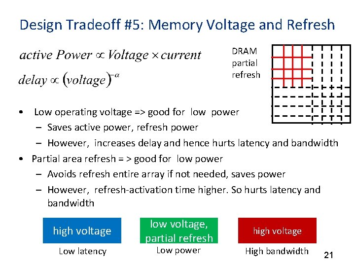
Design Tradeoff #5: Memory Voltage and Refresh DRAM partial refresh • Low operating voltage => good for low power – Saves active power, refresh power – However, increases delay and hence hurts latency and bandwidth • Partial area refresh = > good for low power – Avoids refresh entire array if not needed, saves power – However, refresh-activation time higher. So hurts latency and bandwidth high voltage Low latency low voltage, partial refresh Low power high voltage High bandwidth 21

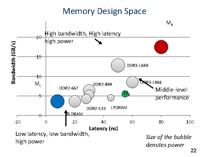
Memory Design Space 25 Bandwidth (GB/s) 20 MB High bandwidth, High latency high power 15 DDR 3 -1600 10 ML DDR 2 -667 MP 5 -20 0 RLDRAM 0 20 DDR 3 -1066 DDR 2 -800 DDR 2 -533 40 LPDRAM Latency (ns) Low latency, low bandwidth, high power Middle-level performance 60 80 100 Size of the bubble denotes power 22

Outline • • • Motivation Memory Design Classifying Applications Using MLP Results Conclusions 23

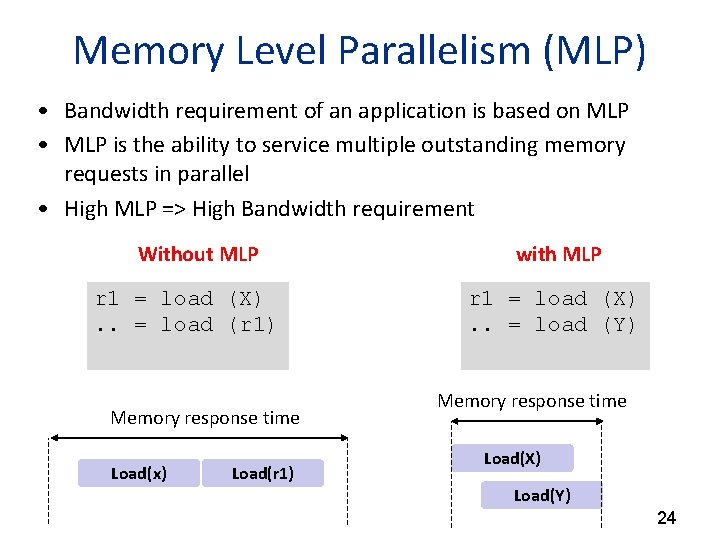
Memory Level Parallelism (MLP) • Bandwidth requirement of an application is based on MLP • MLP is the ability to service multiple outstanding memory requests in parallel • High MLP => High Bandwidth requirement Without MLP r 1 = load (X). . = load (r 1) Memory response time Load(x) Load(r 1) with MLP r 1 = load (X). . = load (Y) Memory response time Load(X) Load(Y) 24

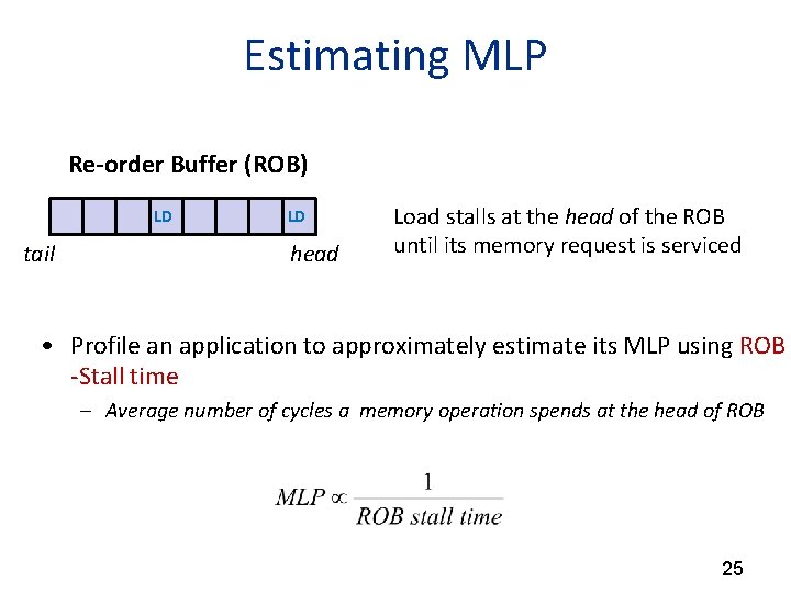
Estimating MLP Re-order Buffer (ROB) LD tail LD head Load stalls at the head of the ROB until its memory request is serviced • Profile an application to approximately estimate its MLP using ROB -Stall time – Average number of cycles a memory operation spends at the head of ROB 25

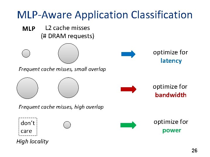
MLP-Aware Application Classification MLP L 2 cache misses (# DRAM requests) optimize for latency Frequent cache misses, small overlap optimize for bandwidth Frequent cache misses, high overlap don’t care optimize for power High locality 26

Page Allocation for Heterogeneous Memory Modules Offline profiling (memory requirement) Classify applications into 3 types 27

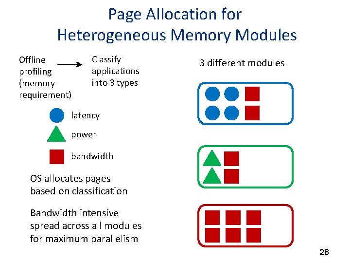
Page Allocation for Heterogeneous Memory Modules Offline profiling (memory requirement) Classify applications into 3 types 3 different modules latency power bandwidth OS allocates pages based on classification Bandwidth intensive spread across all modules for maximum parallelism 28

Outline • • • Motivation Memory Design Classifying Applications Using MLP Results Conclusions 29

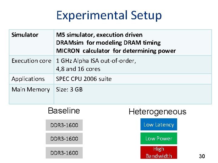
Experimental Setup Simulator M 5 simulator, execution driven DRAMsim for modeling DRAM timing MICRON calculator for determining power Execution core 1 GHz Alpha ISA out-of-order, 4, 8 and 16 cores Applications SPEC CPU 2006 suite Main Memory Size: 3 GB Baseline Heterogeneous DDR 3 -1600 Low Latency DDR 3 -1600 Low Power DDR 3 -1600 High Bandwidth 30

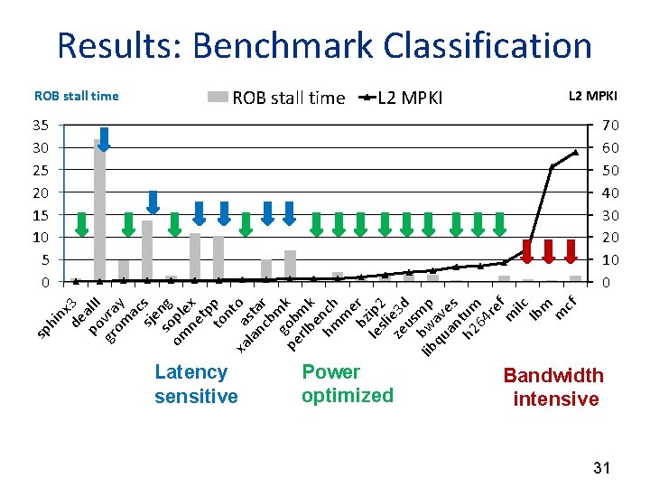
hi nx de 3 po al. II gr vra om y ac sje s so ng om pl ne ex tp to p n xa a to la sta nc r b go mk pe b rlb mk en hm ch m e bz r le ip 2 sli ze e 3 d us m lib bw p qu av an es h 2 tum 64 re m f ilc lb m m cf sp Results: Benchmark Classification ROB stall time Latency sensitive L 2 MPKI Power optimized L 2 MPKI 35 30 25 20 15 10 5 0 70 60 50 40 30 20 10 0 Bandwidth intensive 31

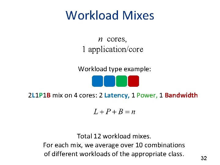
Workload Mixes n cores, 1 application/core Workload type example: 2 L 1 P 1 B mix on 4 cores: 2 Latency, 1 Power, 1 Bandwidth Total 12 workload mixes. For each mix, we average over 10 combinations of different workloads of the appropriate class. 32

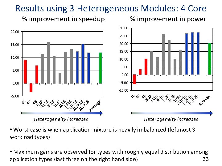
Results using 3 Heterogeneous Modules: 4 Core % improvement in power % improvement in speedup 30. 00 25. 00 20. 00 15. 00 10. 00 5. 00 0. 00 -5. 00 0. 00 4 L 4 P 4 3 L B 1 3 L P 1 3 P B 1 1 L B 3 1 L P 3 1 P B 2 L 3 B 1 1 L P 1 B 2 1 L P 1 B 1 P 2 B Av er ag e -5. 00 Heterogeneity increases 4 L 4 P 4 3 L B 1 3 L P 1 3 P B 1 1 L B 3 1 L P 3 1 P B 2 L 3 B 1 1 L P 1 B 2 1 L P 1 B 1 P 2 B Av er ag e -10. 00 Heterogeneity increases • Worst case is when application mixture is heavily imbalanced (leftmost 3 workload types) • Maximum gains are observed for types with roughly equal distribution among application types (last three on the right hand side) 33

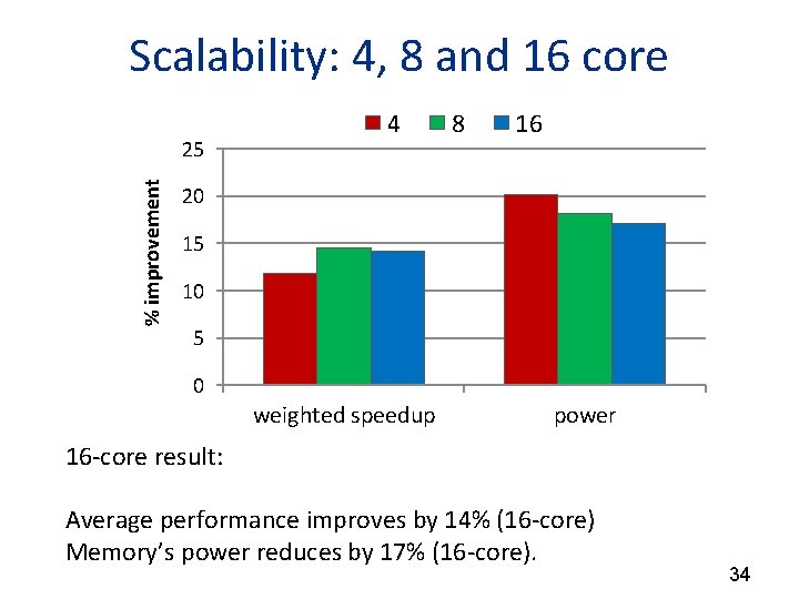
Scalability: 4, 8 and 16 core % improvement 25 4 8 16 20 15 10 5 0 weighted speedup power 16 -core result: Average performance improves by 14% (16 -core) Memory’s power reduces by 17% (16 -core). 34

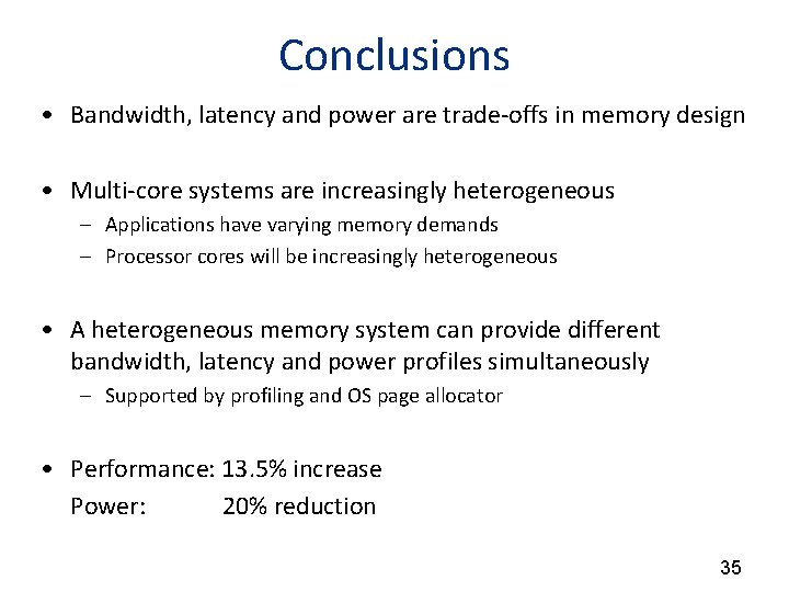
Conclusions • Bandwidth, latency and power are trade-offs in memory design • Multi-core systems are increasingly heterogeneous – Applications have varying memory demands – Processor cores will be increasingly heterogeneous • A heterogeneous memory system can provide different bandwidth, latency and power profiles simultaneously – Supported by profiling and OS page allocator • Performance: 13. 5% increase Power: 20% reduction 35

Thank You! 36