Mixed signal design I Introduction II Analog VLSI


")


 Vy= Vo/k x Vi Vx R 1 K gain of the")

/( K/K) • % change in Q for a")

. B/(s+")


) is")

 Biquad • Also called State-Variable Biquad R’ R’")
 R’ C R’ + Vi QR’ R C BP +")


 R 3 R 2")


| Frequency Sensitivity X X")


: scaling by s L 2 Rs")


 and (C,")


 =")


 •")
 e o e + e o • Correlated double")


/(s. C)")

 Gmi V 1 V 2 Gm 2 + -")


/(1+s/ p)")


 OTA Symbol (b) Implementation")


) is typically expressed in units of d. Bc/Hz • Represents")


 z-1/ (1+z-2) Compar ator X(z) -1 1 z")
 = (1 -z -64 output )/(1 -z-1) input Input")


- Slides: 174
Mixed signal design I. Introduction II. Analog VLSI filters III. RF CMOS basics P. V. Ananda Mohan Fellow IEEE CDAC, Bangalore. 15 June 2017.
A typical DSP based System Analog I/F Band Limiting Filter A/D Smoothin g filter A/D DSP
• A modern CMOS RF receiver (IEEE Solid. State Circuits Magazine Spring 2015)
Anti-Aliasing or band limiting filter for telephony • Example: PCM filter for telephony 3. 4 KHz 4. 6 KHz od. B -32 d. B 300 Hz 4 KHz 50 Hz and harmonics rejection needed in telephony,
DTMF Receivers • Any Button pressed generates one column and one row frequency Row frequencies 697 770 825 1477 1336 Column Frequencies 1209 941
Bandpass Filter+FWR+LPF Low Group Filter L O G I C AGC Input High. Group Filter Dialled digit
GSM transmitter D/A +Filter A/D Speech encoder GMSK Modulator Outpu 90 t stage PA LO D/A +Filter High Frequency operation needed
• • • Signal conditioning –what it means Amplification Attenuation Filtering Isolation Excitation Linearization Sampling Multiplexing Coding (A/D conversion)
Open-loop type Sample and Hold S 1 + + S 2 CH Ts Sampling frequency = 1/Ts • Zero-order hold H(s) = (1 -e-s. T)/s , H(j ω )= Sin (ωT/2)/(ωT/2)
Smoothing filter Smoothed output Stair case type output of D/A Effect of Sample and hold is droop in frequency response Sinx/x. Correction needed for Sinx/x in smoothing filter. 2. 6 d. B
Filter Design Choices • • • Active RC Switched-Capacitor OTA-C Current –mode Digital
Design Requirements • • • Power Consumption Supply Voltage Requirement for clock (in case of SC filters) Dynamic Range (noise floor/distortion) Frequency of operation Area -Total capacitance, Resistance, opamps Sensitivity (Process , Voltage and temperature (PVT) variation) Tuning to achieve required specifications Spread of capacitors/ resistors/ transconductance values Ease of Design (without needing experts) Programmability
Options for structures • Cascade design • Ladder Filters • Component simulation based or operational simulation based
Cascade Design of Filters • Useful for realizing complex high-order responses by cascading several second-order and first-order filters output 1 input 2 n
First-order Filters C R V 0 Vi C Vi V 0 R
All-pass filters R R Vi R V 0 -Vi - Vi C + R V 0 C Needs one inverting amplifier, Floating capacitor R R V 0 Needs Grounded capacitor - Vi + C R Needs Floating capacitor
Transistor based designs for low power and minimum area • First-order All-pass delay cell (2013 IEEE Trans. CAS II Garakoui et al. )
First-order All-pass filter • Low pass type response, delay is 2τ
Differentiators and Integrators Lossless and Lossy R C - Vi + R + Vi V 0 R 2 R - Vi C 1 C - C 2 Vi + R 1 C + V 0
Negative resistance Circuits R 1 Vi R R - + + -R 1 R R Vi R 1 -R 1
Non-inverting integrators Negative resistance R R Deboo Integrator - Uses Negative resistance + Grounded capacitor Vi R V 0 R Needs one opamp only C Vi R + R R + C V 0 Needs Two Opamps
R V 1 - V 2 C + R C Vo= (V 2 -V 1)/s. CR C R Vi V 0 Differential Integrator Needs Matching, balanced Differential output also. - -Vi Differential Integrator Needs Matching of two time constants + R -V 0 C Vo=Vi/s. CR
Fully Differential opamp • Does not give balanced outputs (Vout+ may not exactly equal Vout-)
• Banu, Khoury, and Tsividis, IEEE JSSC, Dec 1988
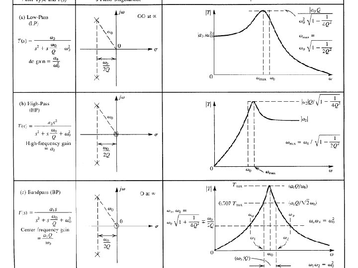
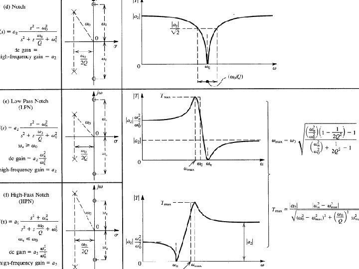
Second-order filters • Second-order transfer function also is expressed in standard form as • • Qz , z are zero-Q , zero frequency Qp , p are pole-Q and pole frequency p/Qp is the bandwidth K is gain
Second-Order Transfer Functions Various types of second-order transfer functions Low-pass n 2=0, n 1=0 High-pass n 1=0, n 0=0 Band-pass n 2=0, n 0=0 Symmetric Notch or Null n 1 = 0, n 0 = n 2 Low-pass Notch n 1=0, (n 0/n 2)>(d 0/d 2) ωz > ωp High-pass notch n 1=0, (n 0/n 2)<(d 0/d 2) ωz < ωp All-pass (n 1/n 2) = (-d 1/d 2), (n 0/n 2) = (d 0/d 2), ωz = ωp, Qz = -Qp
s-domain Unstable Region Real Stable Region Imaginary Marginally stable
Sallen-Key Filter (1955) Vy= Vo/k x Vi Vx R 1 K gain of the amplifier y R 2 Vo C 2 C 1 • Write two KCL equations at x and y nodes
Sallen-Key Filter • Funda: Sensitivity to passive components always shall be on actual expressions and not on simplified version to get correct picture
Sensitivity • SQK = ( Q/Q)/( K/K) • % change in Q for a percentage change in K • Also defined as (d. Q/d. K). (K/Q) • Defined for o also. • e. g. o = 1/(C 1 C 2 R 1 R 2)1/2 • S o C 1 = -½.
Frequency scaling • Filter design tables give in terms of normalized frequency of 1 rad/sec (you can deal with small numbers). At the end, scaling can be done • Butterworth second-order example
Non-ideal Opamp • Finite Bandwidth • Single-pole model Va + Vb Vo Vo=(Vb-Va). B/(s+ a) B unity Gain Bandwidth a is the first pole
Three pole model of the Opamp First Differential gain stage/Frontend Second Differential Gain stage and Frequency compensati on Level Shifter / third gain stage
Effect of Non-ideal OA • Parasitic poles as many as the number of OAs are introduced • Q-enhancement and Pole-Frequency reduction are the result.
R R + Gain = -1 • What are the bandwidths? + Gain = 1
Effect of Opamp Bandwidth on Differentiator - Vi C -Vos/B R + Vo • A second-order band-pass filter and not a first-order high-pass filter !!!!!!
Analysis of effects of OA pole Substitute 1/ ωo. Q (1/(ωo. Q)) is same. Hence (ΔQ/Q)= -(Δ ωo/ ωo) Result is decrease of o and increase of Q. Approximation valid for High-Qs (Akerberg-Mossberg Approximation) Sometimes system may oscillate.
Active-Gm-RC R 2 Vi R 1 C 1 + Vo • Also known as Partially Active R (K. R. Rao et al, Ananda Mohan, D’Amico et al) • Internal Dynamics of Opamp is used (i. e. finite Bandwidth) • Tuning needed • Performance depends on Power supply, tolerances, Bandwidth of Gm block
Kerwin, Huelsman and Newcomb (KHN) Biquad • Also called State-Variable Biquad R’ R’ C R - VZ - + Vi Vx R 1 R + Vy R 2 C + V 3
Tow-Thomas Biquad (Two-Integrator Loop) R’ C R’ + Vi QR’ R C BP + R R’ LP + Rc Rb Ra + Rf Biquadratic Transfer Function
Programmable integrator resistor
Filter design Flow Chart Specification Synthesis of Transfer Function Choice of implementation Choice of component values Scaling For optimal dynamic range. Ordering, Pole-zero pairing Use filter design programs, Tables Cascade, ladder etc, number of Opamps, area etc
Butterworth Filters
Chebychev Filters
Comparison of Responses of various types
Group delay versus frequency • Delays of Fourth order filters
7 th order low-pass elliptic filter
Noise in Filters • Dynamic range depends on Noise Floor • Noise is due to resistors and active devices such as OAs, OTAS. • Resistors have Johnson noise • Noise expressed as noise spectral density • Resistor R has noise spectral density en 2= 4 k. TRB where k is Boltzmann’s constant, B is the bandwidth of measurement, T is the absolute Temperature R en 2= 4 KTRB In practice B is the effective bandwidth decided by the circuit around the resistor
OA noise in 1 eni + in 2 • Noise currents, Noise Voltages • Currents cause effect based on Resistances in the circuit through which they flow • MOS Oas have high 1/f noise (more at low frequencies)
Noise Analysis R 2 R 1 e. R 1 C in 1 eni e. R 2 + in 2 • Four transfer functions for four noise sources Vo
OA OFFSET Model and compensation R 2 R 1 + Voff + R 1. R 2 / ( R 1+ R 2) • Offset currents shall develop equal voltage at both the inputs of OA. • Offset shall be low for maximum dynamic range. • Noise increases because of noise of Offset Compensating resistors!!!
Second order active R filter (State -Variable - Schaumann) R 3 R 2 Vi R 1 R 4 + Vo 1 + - Vo 1 R 5 Vo 2 • Based on Two-Integrator loop. • No capacitors; Unfortunately performance dependent on bandwidth of OPamp which is not controolable.
Active-Gm-RC R 2 Vi R 1 C 1 + Vo • Also known as Partially Active R (K. R. Rao et al, Ananda Mohan, (1979) , rediscovered by D’Amico et al 2006) • Internal Dynamics of Opamp is used (i. e. finite Bandwidth) • Tuning needed • Performance depends on Power supply, tolerances, Bandwidth of Gm block
Filters based on Ladder filters • Doubly terminated filters have low sensitivity to component variation • Orchard’s argument • At the points of inflection, derivative of transfer function is zero and hence sensitivity is zero. Hence, having many such points of inflection, we can reduce the sensitivity in between also to be as small as possible
Sensitivity of Doubly terminated filters |H(j )| Frequency Sensitivity X X
Filters based on Ladder Filters • Component simulation (replace inductor by a simulated inductor block) • Operational simulation (Realize the internal dynamics or nodal equations)
Third order low-pass filter L 2 Rs Vo Vi C 1 C 3 RL • Floating inductance is a headache to realize.
Component simulation using FDNR (frequency dependent Negative resistance): scaling by s L 2 Rs Vo Vi C 1 R 2 Cs FDNR Symbol C 3 RL Vo Vi D 1 D 3 CL
GIC –Generalized impedance converter + - Zin Z 1 Z 2 Z 3 Z 4 - + Z 5
Rs L 2 V 1 Vo Vi C 1 RL C 3 Vi R R - + R R Rs C 2 - + R + - RL L 2 C 3 - + -V 1 R R V 0
Third-order elliptic low-pass filter C 4 L 2 Rs Introduces Transmission Zeroes Vo Vi C 1 RL C 3
Elliptic filter equivalent V 1 Rs L 2 Vo Vi C 1 Vo. C 4/(C 1+C 4) C 3 RL V 1. C 4/(C 3+C 4)
Optimization in Frequency Domain 65
SC Filters
A typical SC filter based system Smoothing filter Band-limiting filter Active RC Filter ANALOG INPUT Active RC filter SCF Sampling Frequency Digital OUTPUT
SC Filters • Use a Switched Capacitor to realize a resistor q 1 q 2 V 1 1 V 2 2 q 1=C(V 1 -V 2) I= q 1/T= C(V 1 -V 2)/T R=T/C C
SC Filters • Resistance is decided by a capacitor value and Sampling period • Time constant R 1 C 2 =T(C 2/C 1) depends on the ratio of capacitors not on absolute values • small capacitors can realize large resistors example 0. 1 p. F capacitor 1 MHz sampling frequency realize resistance of 10 MOhms!
Cptop SC Filters C • Shall be parasitic-insensitive • Mature Technology • Cascade Design, ladder Filter based possible • First-order and Second-order blocks standard designs available • SPICE based simulation Possible • Needs knowledge of DSP (sample-data systems) Cpbot
1 C 2 Vi Vo C 1 2 Stray-Insensitive Inverting Integrator 1 2
1 C 2 Vi Vo C 1 2 Stray-Insensitive Non-inverting Integrator 1 2
C 3 1 C 2 Vi Vo C 1 2 Stray-Insensitive Inverting Damped Integrator 1 2
Analysis of SC networks using Charge Conservation equations q 2 e C q 1 e V 1 q 10 q 1 e =C[(V 1 e-V 2 e)-(V 1 o-V 2 o)z-1/2] q 1 o =C[(V 1 o-V 2 o)-(V 1 e-V 2 e)z-1/2] q 2 e =C[(V 2 e-V 1 e)-(V 2 o-V 1 o)z-1/2] q 2 o =C[(V 2 o-V 1 o)-(V 2 e-V 1 e)z-1/2] V 2 q 2 o
Laker’s z-domain Equivalent of a Switched-Capacitor q 1 e V 1 e q 2 e V 2 e C Cz-1/2 V 1 o q 10 -Cz-1/2 C Cz-1/2 V 2 o q 2 o
Opamp • Each OA becomes two OAs one in odd phase and another in even phase
1 C 2 Vi C 1 2 Voe + Vie C C -Cz-1/2 C -Cz-1/2 -Cz-1/2 C + Cz-1/2 Voo
Simplify and analyse + Vie Voe C -Cz-1/2 C Cz-1/2 + Voo
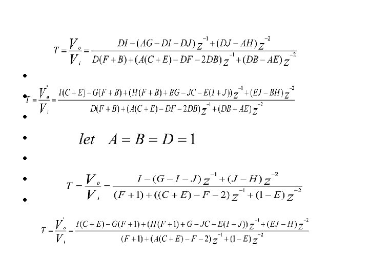
Fleischer-Laker Stray-Insensitive Biquad F E D Vi C B A + G H + T’ output Vo T output I J
Z-domain equivalent of Fleischer-Laker SC Biquad • Lovering’s Active RC configuration
SC Filters • Fleischer-Laker Biquad standard Design • Scaling for minimum total Capacitance possible to reduce the area • Scaling for optimal dynamic range Possible • Two Types E Circuit, F Circuit • Two Outputs T and T’ held over a clock period- easy cascadability • Four options T and T’ output E and F types • Feed-Forward four degrees of freedom G, H. I. J
Simple choices to avoid matching Examples High-Pass Filter: H=0, J=I, G=4 I Numerator: 1 -2. z-1 -z-2 Band-Pass Filter Bilinear : J=0, I=H, G=H Numerator 1 -z-2 Notch Filter: H=0, J=I, G=I(2 -a) 1 -az-1+z-2
Design Procedure • • • Start with A=B=D=1 Choose E or F circuit Choose T or T’ output Match the coefficients to determine E (or F), C Determine G, H, I and J only three are needed. Use simple choices which do not need matching Combine capacitors if possible. Reduce the number of switches. Find maxima of T and T’ thus realized. Scale to equalize the maxima.
Simplifications G + H=G G + • G=H say then use an unswitched capacitor G. Same applies to I=J also.
Minimum Switch SC biquad G + H=G +
Design Procedure • Consider two groups (A, B, F, I and J) and (C, D, E , G and H). • Denote the smallest in each group as unity and sale all others accordingly. • Find the total capacitance and capacitance spread • Compare the circuits and find the biquad with minimum area.
Example of Capacitance Scaling • • • A=10, B=0. 1, F=2, I=2. 5, J=0. 25 Minimum of these is 0. 1. Call this Cu. Divide all others by this value: A=100 Cu, B=Cu, F=20 Cu, A=25 Cu, A=2. 5 Cu Thus total capacitance is 148. 5 Cu. Capacitance spread is 100.
S domain to z domain Imaginary axis of splane mapped to unit circle ω fs/2 stable R θ 0 σ -σ -fs/2 stable -ω Outside the unit circle is the unstable region
Basic Relationships • Z = es. T • S=-σ+jω • Z = e(-σT+jωT) = e-σT e+jωT = e-σT (cos (ωT)+j sin (ωT)) = R (cos θ+ j sin θ) = Rejθ • S-domain complex roots (-σ+jω), (-σ-jω) • Z-domain Rejθ, Re-jθ • Quadratic factor in s-domain is s 2+2 σs+ (σ2+ω2) • Quadratic factor in z-domain is (z 2 -2 Rzcosθ+R 2) or (1 -2 Rz-1 cosθ+R 2 z-2)
Frequency Transformations • Desirable • Stable Analog to stable digital • Frequency response from 0 to Infinite frequency of analog shall be preserved. • Based on Numerical integration
s domain to z domain Frequency Transformations S domain z domain Mapping rule Tranformation used Comments Analog frequency Digital frequency z = e(σ+jω)T z = es. T Aliasing 0 to ∞ 0 to fs/2 Unique mapping Bilinear Transformation 0 to fs/π 0 to fs/2 LDI (lossless discrete Integration) Not defined properly 0 to fs/2 Not defined properly Forward Euler Transformation Not defined properly 0 to fs/2 Not defined properly Backward Euler transformation
Third Order SC filter based on LC ladder filter - + + - • Cross-coupling capacitors needed only for elliptic filters • Design can be LDI type or Bilinear Transformation type
Noise model Switch RON en 2 C • Noise is wideband hence depending on fs, noise in higher bands gets folded into the passband. • Noise of a SC: en 2= k. T/C • Proof: en 2 =4 k. TR. (1/4*R*C)=k. T/C • Use as large capacitances as possible!
SC Technique- Issues • Need for a sampling clock • Switch noise fold-over depending on the sampling frequency • Analog-Intensive • Simulation and Design tools available • Anti-aliasing filters • Clock Feed-through effects
SC FIR filters 2 1 3 3 1 + 1 3 Delay circuit using three phase clock • Real Time FIR filtering possible i. e. one clock cycle weighting of samples and accumulation! • Uses SC delays
Capacitor layout • Use centroid geometry. • Smallest capacitor is called unit capacitor • This has minimum feature size W=L.
Limitations of SC filters • Clock Feed-through results as offset (due to aliasing) • Switch noise (wideband) Fold-over (due to sampling frequency being limited) • Need For Clock Frequency (not a real problem in a digital world) • Need for Anti-aliasing and Smoothing filters
Offset compensation Scheme (Gregorian) e o e + e o • Correlated double sampling: Sample the offset in one half cycle and subtract in the next from the offset, Result: (1 -z 1/2) Transfer function. Noise and clock feedthrough also gets cancelled! • Sped is a problem since one half-cycle is needed to discharge.
Switch S G D
Switch Non-idealities • Clock Feed-through • NMOS transistor shunted by PMOS transistor reduces clock feed-through • Effect is to cause dc offset due to aliasing! • Differential circuits recommended • Duplicated hardware • Noise of switch due to ON resistance as well as 1/f noise
Methods of suppressing Charge injection Clock Inverted Clock S 1 • Dummy switch compensation • Partial improvement possible • S 2 is half the width of S 1. S 2
MOS SWITCH Vov = VGS-Vth is called overdrive. Example: W = L, Vov = 1 V, then Ron, n = 8. 4 Kohms and Ron, p = 25. 6 Kohms Rule: Drive should be at least a threshold voltage higher than the input signal.
SC Technique- issues • Need for a sampling clock • Switch noise fold-over depending on the sampling frequency • Analog-Intensive • Simulation and Design tools available • Anti-aliasing filters • Clock Feed-through effects
OTA-C FILTERS
OTA-C FILTERS •
OTA-C filters • Operational Transconductance Amplifier • Continuous-time operation • Tuning of OTAs needed using Sophisticated techniques. • Quite Popular, state-of-the-art • Programmable characteristics using digital control
OTA Symbol V 1 V 2 + - Gm is transconductance I = Gm. (V 1 -V 2)
Amplifier Differential V to I converter V 1 Vo + V 2 gm 1 + gm 2 Resistor =1/gm 2
OTA-C and Active RC Integrators V 1 Vo =Gm. (V 1 -V 2)/(s. C) + - V 2 C R 1 V 2 C 2 + V 0 R 2 C 1 • See how simple it is, no matching needed
First-order OTA-C filter Example Resistor V 1 Vo + V 2 C gm 1 + Low-Pass Filter gm 2
Second-Order OTA-C Filter (Two-Integrator loop) Gmi V 1 V 2 Gm 2 + - Gm 3 + - - - + C 1 Lossless integrator + C 2 Gm 4 Lossy Integrator • Uses grounded capacitors, canonic, • Frequency control through Gm 2, Gm 3, C 1, C 2, • Q Control through Gm 4 Gain control through Gm 1
Inductance simulation using OTAs V 1 V 2 - + Gm 1 - + Gm 2 C 1 • L = Gm 1 Gm 2/C 1 Gm 3 - +
Third order Elliptic Filter Realization C 4 Rs Vi L 2 C 1 Vo RL C 3 Rs + Vi Vo C 4 C 1 - + C 3 - + + RL C 3’
OTA non-idealities • Pole-zero model to characterize frequency response • Gm=Gmo. (1+s/ z)/(1+s/ p) • Zero can be greater or lesser than pole frequency or equal the pole frequency • OTA has finite output and input impedances Ri shunted by Ci or Ro shunted by Co. Ci or Co directly affects the actual capacitance.
Tuning techniques
Tuning techniques • Needed to bring the OTA Gms or MOSFET resistor values to the desired value • Uses Master slave techniques • Can be on-line or Off-line • Can be based on oscillators or filters or calibrating resistors
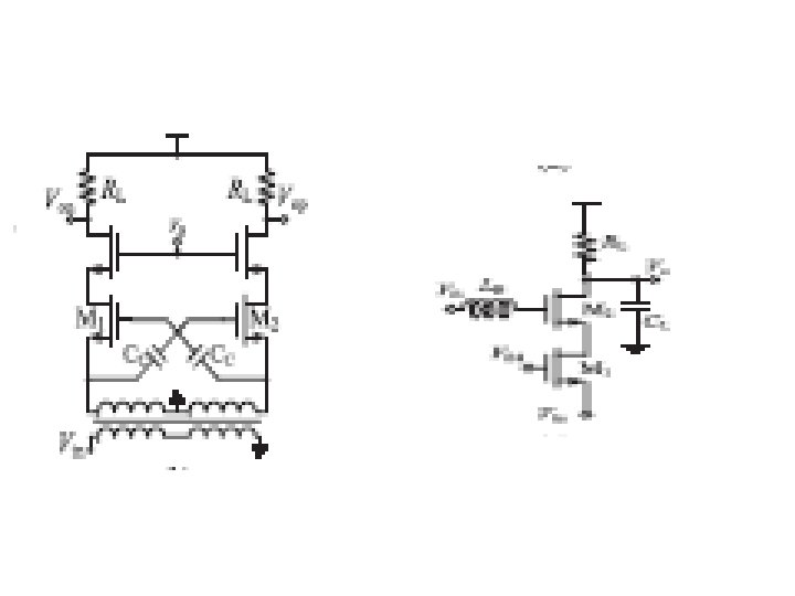
Tuning Techniques output F I L T E R input F F I IL L T T E E R R input Ro Vc Comparison circuit output Filter Vc Comparison circuit FILTE R Rext Clock FILTER F I L T E R input Oscillator output Vc OSC Comparison circuit FILTER Clock
Tsividis –Banu Tuning technique Clock Voltage controlled Oscllator Voltage comparator Vc Vc - + + - Voltage comparator Vc Vc in in Elliptic Filter +Single ended to differential input converter Out+ Out- Loop Filter Phase Detector
Continuous-Time filters
CONTINUOUS-TIME FILTERS • Use MOSFETs to realize resistors • Still need Opamps (Differential input differential output ) • Need Frequency and Q control loop using master slave technique due to Radhakrishnarao and Srinivasan.
MOSFET-C Integrator Vin C Vo C -Vo Vc + -Vin -Vc • Distortion of the MOS transistors is cancelled by the differential arrangement. (even-order nonlinearities cancel) • MOS transistor is used as a resistor
General first-order MOSFET-C circuit - + + - • Voorman’s extension of Ananda Mohan MOSFET-C filter
Parameters of a 0. 25 μM CMOS opamp Feature Value Unit DC gain 80 d. B CMRR 40 d. B Offset 4 -6 m. V Bandwidth 100 MHz Slewrate 3 V/microsecond Settling time 1 V, CL-4 p. F 300 Nsec PSRR dc 90 d. B PSRR @1 KHz 60 d. B PSRR@ 100 KHz 30 d. B Input referred noise(white) 100 Nv/root Hertz Corner Frequency 1 k. Hz Supply voltage 3. 3 V Input common mode voltage 1. 5 V Output dynamic Range 2. 2 Vpp Power Consumption 1 m. W Silicon Area 2000 Square micrometers
TWO-STAGE AMPLIFIER MB M 6 M 7 IBIAS M 1 M 3 M 2 M 3 CC Out M 5
• (a) OTA Symbol (b) Implementation
• Yang and Roberts Nov. 2016 TCAS I pp 1794 -1806. gm 40 µA/V to 60µA/V variable
A MOS comparator Combining gain stage and latch VB 2 M 3 Out- M 4 In. In+ M 1 Out+ M 2 M 6 M 5 Strobe bar M 7 M 8 Strobe VB 1 M 9
RF CMOS
• · Amplification to compensate for transmission losses • · Selectivity to separate the desired signal from others • · Tunability to select the desired signal • · Conversion to digital domain
• Adapted from A. Liscidini, IEEE Solid. State Circuits Magazine, Spring 2015, pp
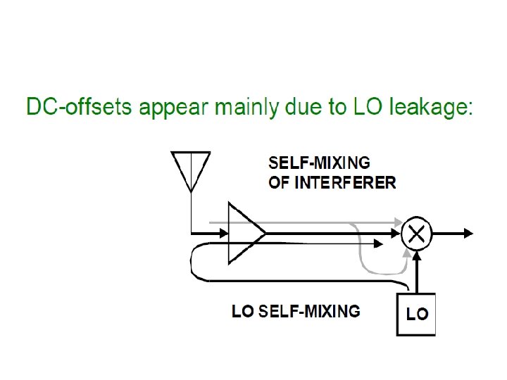
• Difficulties in implementation: dc offsets, leakage between RX and TX in full duplex operation
Distortion • Nonlinearity is evaluated by Taylor series expansion of output versus input • The resulting four components obtained by feeding two tones ω1 and ω2 are • + • First two are fundamentals i. e frequencies that are fed. a 1 is the linear gain of the system for these. The last two are proportional to a 3.
1 d. B compression point • Indicates linearity of the PA. Input power versus ouput power.
Distortion-Third-order intercept • 2ω2 -ω1, 2 ω1 -ω2 are called third-order intermodulation products. • Fundamentals and IM 3 tones are equally spaced. • Fundamental grows with a slope of 1. • IM 3 grows with a slope of 3. • The curves can intercept each other at a point called third-order intercept even though IM 3 amplitudes are lower. • Note that the curves bend for large amplitude inputs. • Third-order intercept is an extrapolated point.
• Higher the AOIP 3, it is linear upto larger signal input level
• Input amplitude at which third order intercept occurs is
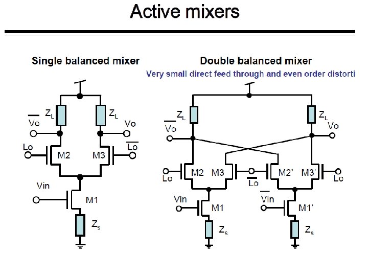
Passive Mixers • Using 2 -phase LO, the polarity of the input signal is reversed half the time implying multiplication by a square wave.
Fris’ formula for noise of cascaded stages First stage contributes more noise than other stages. Hence LNA is required to reduce first stage noise.
CG and CS type Low Noise Amplifiers • CG LNA – input matching easy, Noise Figure more (Zin = 1/gm 1) • CS LNA= Impedance matching difficult, Noise Figure less
Gm boosted CG-LNA
• Ma, Wang, Xu and Amin IEEE TCAS II April 2017.
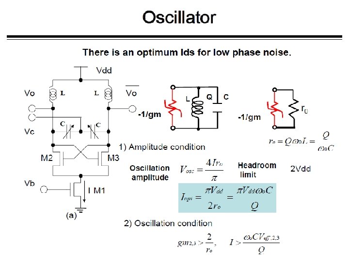
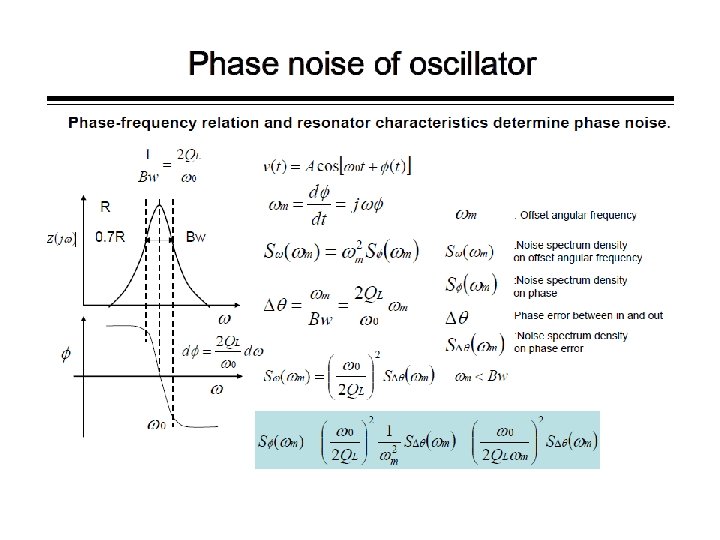
Phase Noise • (ℒ(f)) is typically expressed in units of d. Bc/Hz • Represents the noise power relative to the carrier contained in a 1 Hz bandwidth centered at a certain offsets from the carrier. • Leeson Equation: • Phase noise can be reduced by having high Q resonator and/or large gain
Modern codec-filter • Very small analog part!!! Three opamps , Few SC, frw Capacitors and resistors. Active RC Filter input SIGMA -DELTA Converter Over sampling Clock Decimation Digital Filter clocks Digital output
n First-Order Sigma Delta Modulator Difference amplifier V 2 V 1 + Integrator I bit DAC Vref Consider Ain=0. 2 volts and Vref=1 volt. Sample Number V 1 V 2 V 3 Dout Comparator 1 . 2 1 1 2 -. 8 -. 6 0 - 1 + 3 1. 2 . 6 1 1 4 -. 8 -. 2 0 - 1 5 1. 2 1. 0 1 1 6 -. 8 . 2 1 1 7 -. 8 -. 6 0 -1 8 1. 2 . 6 1 1 9 -. 8 -. 2 0 -1 Average of Dout = (-1+1+1)/5=1/5=0. 2 Result for 20 samples Inputvolts Sequence of output bits 0. 0 0 1 0 1 0 1 0. 1 1 0 1 0 1 0. 2 1 0 1 0 1 0. 7 1 1 1 0 1 1 1 0. 9 1 1 1 1 1 0 1 1 1. 0 1 1 1 1 1
What is a sigma-delta converter? compar ator + Integrator cloc k + input latch Small analog circuitry-Rest Digital output
Quantization noise in passband is low and is more out of band. Filter out by a decimation filter Quantization Noise Signal
Band-Pass Sigma delta Modulator 1/2 Y(z) z-1/ (1+z-2) Compar ator X(z) -1 1 z -1 z -1 • H(z)=z-2 and N(z)=(1+z-2)2 Transmission zeroes at fs/4, Obtained by z-1 to –z-2 transformation.
DECIMATION FILTER EXAMPLE • H(z) = (1 -z -64 output )/(1 -z-1) input Input Stream Accumulator Lower Clock Latch Output word clock
Flash architecture Video A/D Converter Vref input Thermometer code Comparators
CMOS D/A converter 15 C C 2 C VREF 4 C 8 C Digital word 4 bit + V out
Guidelines for Mixed Signal Design • Separate Analog and digital portions as far as possible. • Separate grounds for analog and digital portions • Analog and digital power supplies to be separate • Careful routing of clock • Fully differential analog circuits to reduce effects of digital clocks and clock feed through of analog circuits. • Worry about minimum area designs, sensitivity, noise, dynamic range, power consumption
Digital Analog portion with Guard Bands and Dummy cells
CURRENT-MODE FILTERS
Current Conveyor Vx X Z Y Vy Iy=0, Iz=Ix, Vx=Vy Iz
Integrators using Current conveyors R R Iin X Z Y I 0 C Vin V 0 C Current-mode Voltage-mode
Features • • Simple to design In market, CCs are available (AD 844 front end ) Wealth of knowledge Non Idealities: Finite series resistance at x input, finite output resistance and capacitance to ground at Z output, input buffer finite gain and bandwidth between Y and X inputs • Flexibility: votage or current inputs/ outputs
A single CC based biquad R X Z Y R C R Iin I 0
A CC based Two integrator-loop Biquad I 3 R 2 R 1 I 4 X Z Y I 2 C 1 C 2 R 2
Current Feedback Operational amplifier Vx z X Z Y Iz Vy Internal load Vo
CFOA based Amplifier R 1 R 2 Vi Z X Rx K Iin Ro Co Y • The bandwidth thus is dependent only on the Co and R 2 and not on the gain!
CFOA based oscillator • Uses CFOA pole Y 2 x z y Y 1 Y 3 Y 4 Y 1=s. C 1, Y 2=G 2, Y 3=G 3+s. C 3, Y 4=G 4, ,
Tools Needed • • SPICE, Spectre RF etc, Device modeling Macromodels Mentor Graphics VHDL/Verilog knowledge DSP emulation and simulation tools Microcontroller programming Interface knowledge VLSI Layout, Design rules
Resources • Several books: Laker-Ghausi, Gregorian- Temes, Allen-Geiger, Ananda Mohan-Ramachandran-Swamy, Allen-Sanchez Sinencio, Martin, Deliyannis-Sun-Fidler etc • Jounals: IEEE Journal of Solid-State Circuits, Proc. IEEE, IEEE Transactions on Circuits and Systems, Electronics Letters, IEE Part G, Kluwer Journal of Analog Signal Processing
Conclusion • SOC is the trend • Choice of Technology e. g. Bipolar/CMOS/Bi. CMOS/Si. Ge • Building blocks based approach • Modeling tools • Vast scope for Design if not fabrication
Contact • pvam@vsnl. net • anandmohanpv@hotmail. com