MIT Lincoln Laboratory Magnesium Diboride Films for SRF
MIT Lincoln Laboratory Magnesium Diboride Films for SRF Cavity Applications Y. D. Agassi Naval Surface Warfare Center, Carderock Division, Bethesda MD D. E. Oates MIT Lincoln Laboratory, Lexington MA B. H. Moeckly STI, Inc. , Santa Barbara CA Sponsor: Office of Naval Research (SRF 2011, CHICAGO, JULY ‘ 11) 1
Outline MIT Lincoln Laboratory I. Introduction and Approach: The Need to Go Beyond Bulk-Nb Cavities The T > 4 K Approach: Mg. B 2/{Cu, Nb} Films; Thickness ~2 Properties, Potential Payoffs, Challenges II. The Case for Mg. B 2: ► Reactive Evaporation High-quality Thin-film Deposition ► Rs(T, H) Data Power Dependence (Low, High) ► Film Passivation Film stability ► System Simulations Thermal Management ► Energy Gap Data (IMD, (T < 5 K)) and Theory of Energy-Gap Symmetry III. Summary, Outlook 2
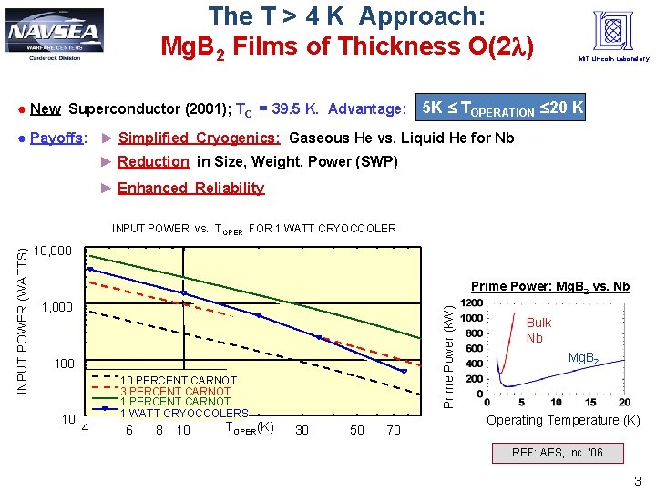
The T > 4 K Approach: Mg. B 2 Films of Thickness O(2 ) ● New Superconductor (2001); TC = 39. 5 K. Advantage: MIT Lincoln Laboratory 5 K TOPERATION 20 K ● Payoffs: ► Simplified Cryogenics: Gaseous He vs. Liquid He for Nb ► Reduction in Size, Weight, Power (SWP) ► Enhanced Reliability 10, 000 Prime Power: Mg. B 2 vs. Nb 1, 000 Prime Power (k. W) INPUT POWER (WATTS) INPUT POWER vs. T OPER FOR 1 WATT CRYOCOOLER 100 10 10 PERCENT CARNOT 3 PERCENT CARNOT 1 WATT CRYOCOOLERS 4 6 8 10 TOPER(K) 30 50 70 Bulk Nb Mg. B 2 Operating Temperature (K) REF: AES, Inc. '06 3
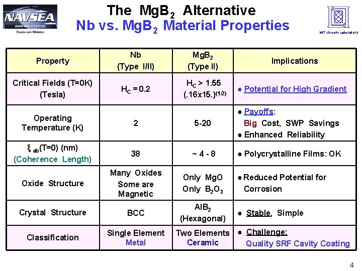
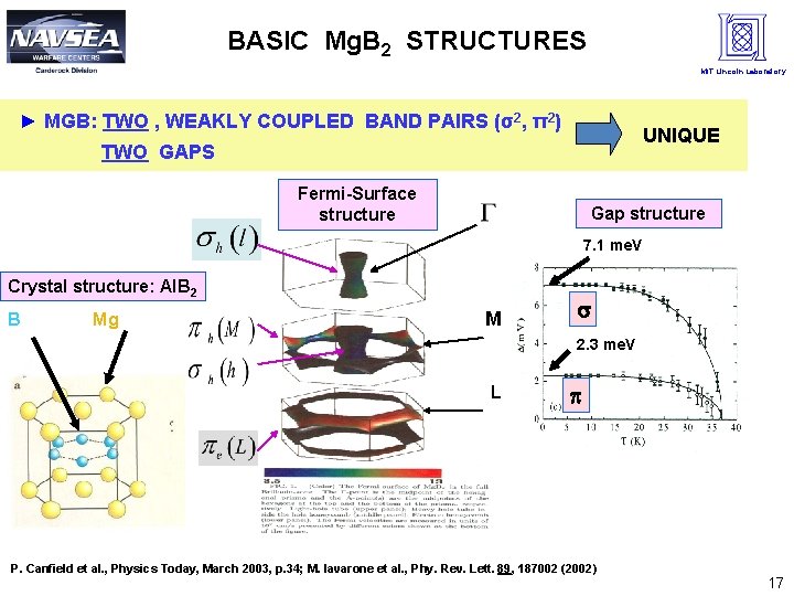
The Mg. B 2 Alternative Nb vs. Mg. B 2 Material Properties Property Nb (Type I/II) Mg. B 2 (Type II) Critical Fields (T=0 K) (Tesla) HC = 0. 2 HC > 1. 55 (. 16 x 15. )(1/2) MIT Lincoln Laboratory Implications ● Potential for High Gradient Operating Temperature (K) 2 5 -20 ● Payoffs: Big Cost, SWP Savings ● Enhanced Reliability ξ ab(T=0) (nm) (Coherence Length) 38 ~4 -8 ● Polycrystalline Films: OK Oxide Structure Many Oxides Some are Magnetic Only Mg. O Only B 2 O 3 Crystal Structure BCC Al. B 2 (Hexagonal) Classification Single Element Metal ● Reduced Potential for Corrosion ● Stable, Simple Two Elements ● Challenge: Ceramic Quality SRF Cavity Coating 4
Outline MIT Lincoln Laboratory I Introduction And Approach: The Need to Go Beyond Bulk-Nb Cavities The T > 4 K Approach: Mg. B 2/{Cu, Nb} Films; Thickness ~2 Properties, Potential Payoffs, Challenges II. The Case for Mg. B 2: ► Reactive Evaporation High-quality Thin-film Deposition ► Rs(t, H) Data Power Dependence (Low, High) ► Film Passivation Film stability ► System Simulations Thermal Management ► Energy Gap Data (IMD, (T < 5 K)) and Theory of -Gap Symmetry III. Summary, Outlook 5
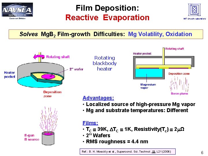
Film Deposition: Reactive Evaporation MIT Lincoln Laboratory Solves Mg. B 2 Film-growth Difficulties: Mg Volatility, Oxidation Rotating blackbody heater Advantages: • Localized source of high-pressure Mg vapor • Mg and substrate temperatures: Different Films: • TC 39 K, TC 1 K, Resistivity(Tc) 2 Ω • 2” Wafers • RMS roughness = 4. 4 nm Ref. : B. H. Moeckly et al. , Supercond. Sci. Technol. 19, L 21 (2006) 6
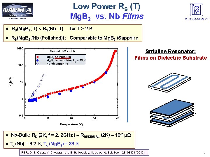
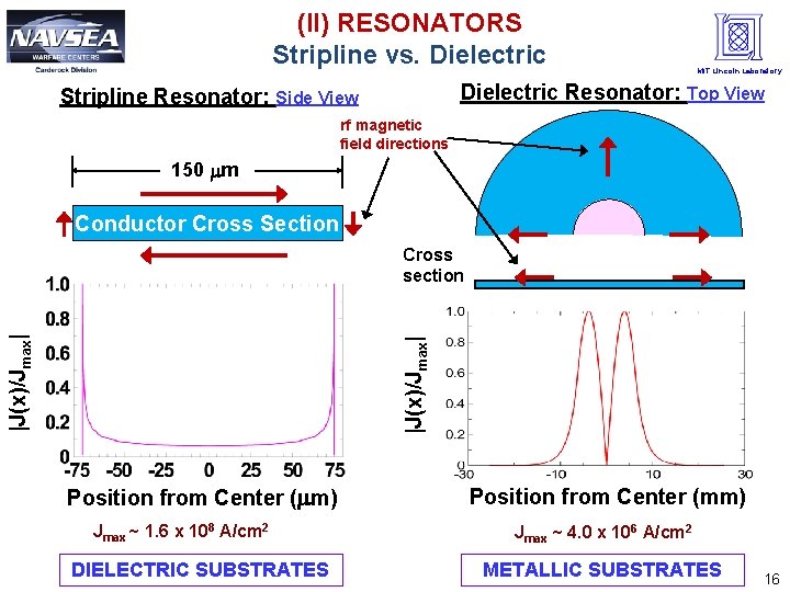
Low Power RS (T) Mg. B 2 vs. Nb Films ● RS(Mg. B 2; T) < RS(Nb; T) MIT Lincoln Laboratory for T > 2 K ● RS(Mg. B 2 /Nb (Polished)): Comparable to Mg. B 2 /Sapphire Stripline Resonator: Films on Dielectric Substrate ● Nb-Bulk: RS (2 K, f = 2. 2 GHz ) RRESIDUAL (2 K) 10 -2 Ω ● Tc (Nb) = 9. 2 K, Tc (Mg. B 2) = 39 K REF. : D. E. Oates, Y. D. Agassi and B. H. Moeckly, Supercond. Sci. Tech. 23, 03401 (2010) 7

Higher Power RS (T) Mg. B 2/(Nb, Sapphire) MIT Lincoln Laboratory Dielectric Resonator Films on Metallic or Dielectric Substrates HC 1 ~ 300 Oe ● Rs(NL Onset)/Sapp. at H ~ 800 Oe ( EACC ~ 20 MV/m): Material Limited? ● RS(NL Onset)/Nb at H > 200 Oe Flat! Equipment Limited ● Sample Variability REF. : D. E. Oates, Y. D. Agassi and B. H. Moeckly, Supercond. Sci. Tech. 23, 03401 (2010) 8
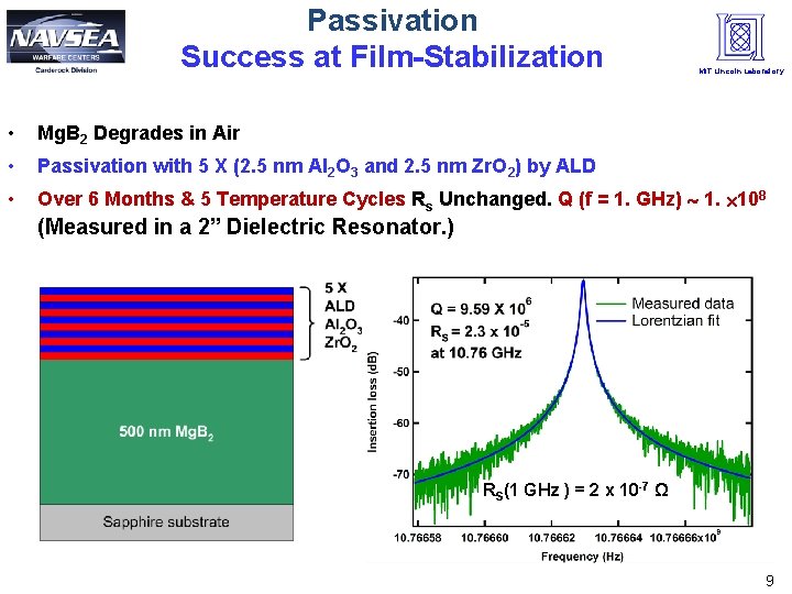
Passivation Success at Film-Stabilization MIT Lincoln Laboratory • Mg. B 2 Degrades in Air • Passivation with 5 X (2. 5 nm Al 2 O 3 and 2. 5 nm Zr. O 2) by ALD • Over 6 Months & 5 Temperature Cycles Rs Unchanged. Q (f = 1. GHz) 1. 108 (Measured in a 2” Dielectric Resonator. ) RS(1 GHz ) = 2 x 10 -7 Ω 9

System Simulations Thermal Management, Power (AES, Inc. ) • MIT Lincoln Laboratory Based on Our RS Data Simulations Confirmed Feasibility Two Thermal-management Issues: 1. Gaseous He Cooling : Mg. B 2/Cu Five-Cavity Array 2. Resonance-Frequency Shift : Due to Thermal Expansion Worst Case Scenario He(T, P) = (30 K, 3 Atm) (Q =. 608 E 9 f = 703. 75 MHz) REF: AES, Inc. • Cooling Load: Not a Problem • Thermal Expansion: Relatively Small Feasible Prime Power (k. W) Prime Power: Mg. B 2 vs. Nb Bulk Nb Mg. B 2 Operating Temperature (K) 10
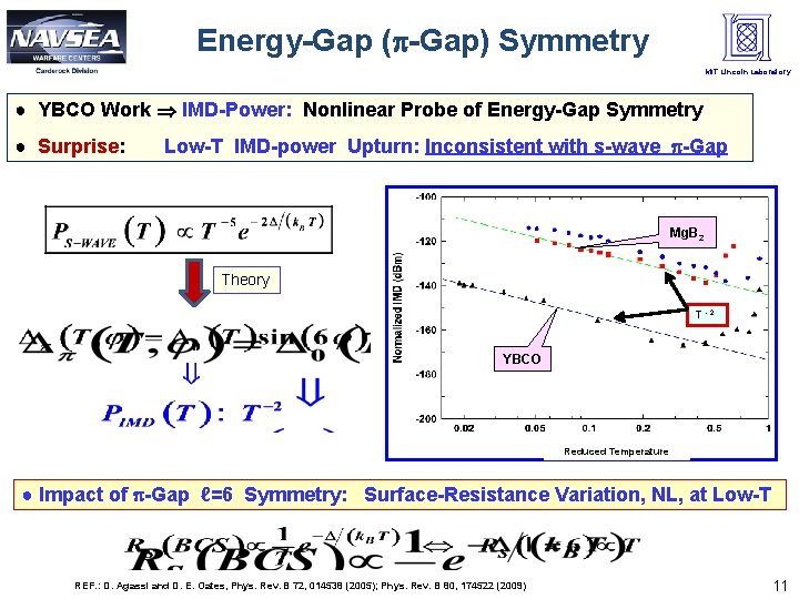
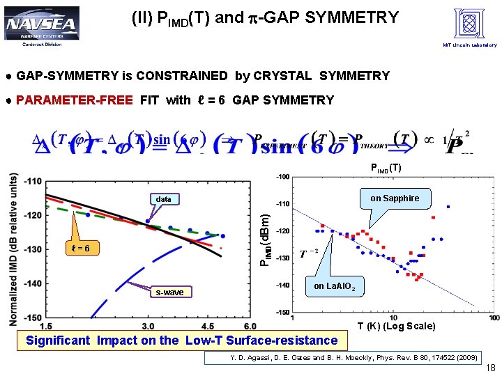
Energy-Gap ( -Gap) Symmetry MIT Lincoln Laboratory ● YBCO Work IMD-Power: Nonlinear Probe of Energy-Gap Symmetry ● Surprise: Low-T IMD-power Upturn: Inconsistent with s-wave -Gap Mg. B 2 Theory T -2 YBCO Reduced Temperature ● Impact of -Gap ℓ=6 Symmetry: Surface-Resistance Variation, NL, at Low-T REF. : D. Agassi and D. E. Oates, Phys. Rev. B 72, 014538 (2005); Phys. Rev. B 80, 174522 (2009) 11
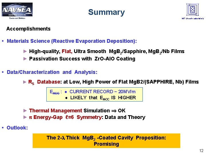
Summary MIT Lincoln Laboratory Accomplishments • Materials Science (Reactive Evaporation Deposition): ► High-quality, Flat, Ultra Smooth Mg. B 2/Sapphire, Mg. B 2/Nb Films ► Passivation Success with Zr. O-Al. O Coating • Data/Characterization and Analysis: ► RS Database: at Low, High Power of Flat Mg. B 2/(SAPPHIRE, Nb) Films EACC : ● CURRENT RECORD ~ 20 MV/m ● LIKELY that EACC IS HIGHER ► Thermal Management Simulation OK ► Energy-Gap ℓ=6 Symmetry: Data and Theory • Outlook: The 2 - Thick Mg. B 2 -Coated Cavity Proposition: Promising 12
Future Challenges MIT Lincoln Laboratory ► High-Quality Film Deposition on Curved Metallic Surfaces ► Demonstrating Low RS in those films ► Demonstrating a High Field Gradient in those Films ► Theory ► Make a Mg. B 2 -based RF Cavity with High Field Gradient 13
MIT Lincoln Laboratory End Presentation 14 14
MIT Lincoln Laboratory Backup Slides 15 15
(II) RESONATORS Stripline vs. Dielectric MIT Lincoln Laboratory Dielectric Resonator: Top View Stripline Resonator: Side View rf magnetic field directions 150 m Conductor Cross Section |J(x)/Jmax| Cross section Position from Center ( m) Jmax ~ 1. 6 x 10⁸ A/cm 2 DIELECTRIC SUBSTRATES Position from Center (mm) Jmax ~ 4. 0 x 106 A/cm 2 METALLIC SUBSTRATES 16
BASIC Mg. B 2 STRUCTURES MIT Lincoln Laboratory ► MGB: TWO , WEAKLY COUPLED BAND PAIRS (σ2, π2) UNIQUE TWO GAPS Fermi-Surface structure Gap structure 7. 1 me. V Crystal structure: Al. B 2 B Mg M 2. 3 me. V L P. Canfield et al. , Physics Today, March 2003, p. 34; M. Iavarone et al. , Phy. Rev. Lett. 89, 187002 (2002) 17
(II) PIMD(T) and -GAP SYMMETRY MIT Lincoln Laboratory ● GAP-SYMMETRY is CONSTRAINED by CRYSTAL SYMMETRY ● PARAMETER-FREE FIT with ℓ = 6 GAP SYMMETRY PIMD(T) on Sapphire PIMD(d. Bm) data ℓ=6 s-wave on La. Al. O 2 T (K) (Log Scale) Significant Impact on the Low-T Surface-resistance Y. D. Agassi, D. E. Oates and B. H. Moeckly, Phys. Rev. B 80, 174522 (2009) 18
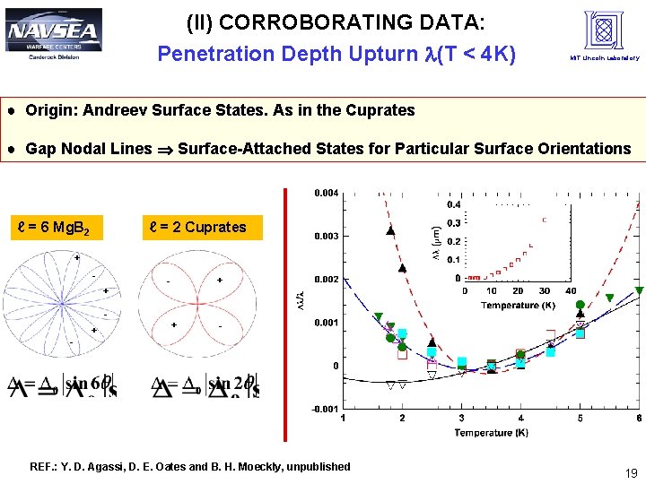
(II) CORROBORATING DATA: Penetration Depth Upturn (T < 4 K) MIT Lincoln Laboratory ● Origin: Andreev Surface States. As in the Cuprates ● Gap Nodal Lines Surface-Attached States for Particular Surface Orientations ℓ = 6 Mg. B 2 ℓ = 2 Cuprates + + - REF. : Y. D. Agassi, D. E. Oates and B. H. Moeckly, unpublished 19
- Slides: 19