MIT 3 071 Amorphous Materials 11 Amorphous Silicon

- Slides: 25

MIT 3. 071 Amorphous Materials 11: Amorphous Silicon Macroelectronics Juejun (JJ) Hu hujuejun@mit. edu 1

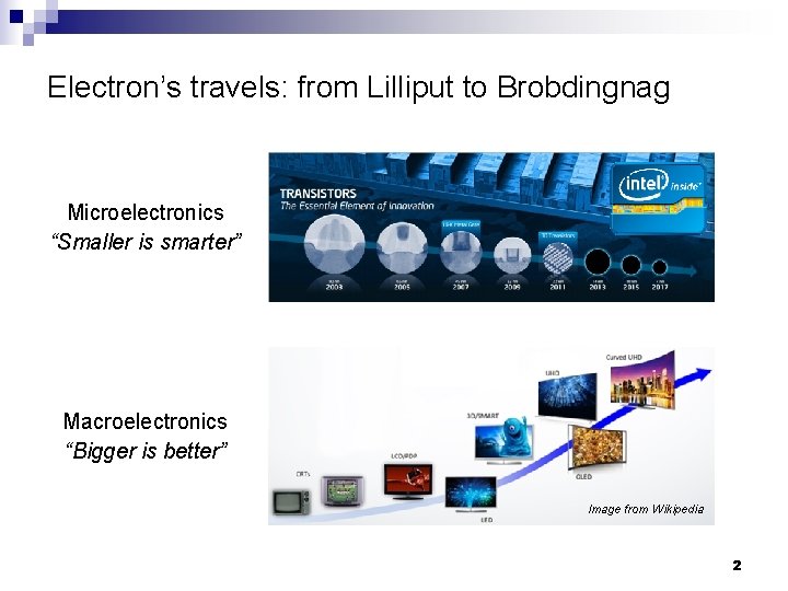
Electron’s travels: from Lilliput to Brobdingnag Microelectronics “Smaller is smarter” Macroelectronics “Bigger is better” Image from Wikipedia 2

Why amorphous silicon? n n Large-area, low-temperature, monolithic deposition ¨ Low-cost, mature plasma-enhanced CVD (PECVD) process ¨ Dielectrics and passivation layers can be formed using the same process Doping capacity ¨ n Effective passivation of defects (hydrogenation) CMOS compatibility ¨ Leveraging existing infrastructure and knowledge base from the microelectronics industry “The essence of being human is that one does not seek perfection. ” -- George Orwell 3

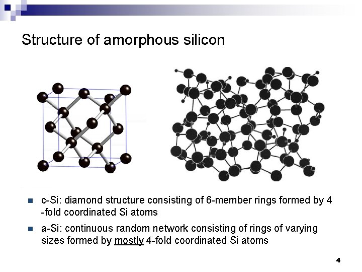
Structure of amorphous silicon n c-Si: diamond structure consisting of 6 -member rings formed by 4 -fold coordinated Si atoms n a-Si: continuous random network consisting of rings of varying sizes formed by mostly 4 -fold coordinated Si atoms 4

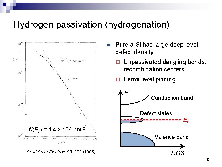
Hydrogen passivation (hydrogenation) n Pure a-Si has large deep level defect density ¨ Unpassivated dangling bonds: recombination centers ¨ Fermi level pinning E Conduction band Defect states EF N(EF) = 1. 4 × 1020 cm-3 Valence band Solid-State Electron. 28, 837 (1985) DOS 5

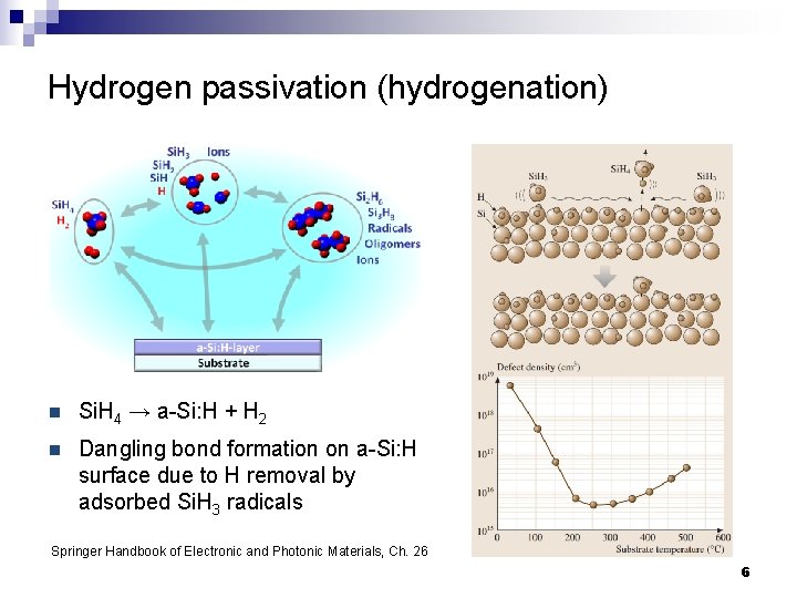
Hydrogen passivation (hydrogenation) n Si. H 4 → a-Si: H + H 2 n Dangling bond formation on a-Si: H surface due to H removal by adsorbed Si. H 3 radicals Springer Handbook of Electronic and Photonic Materials, Ch. 26 6

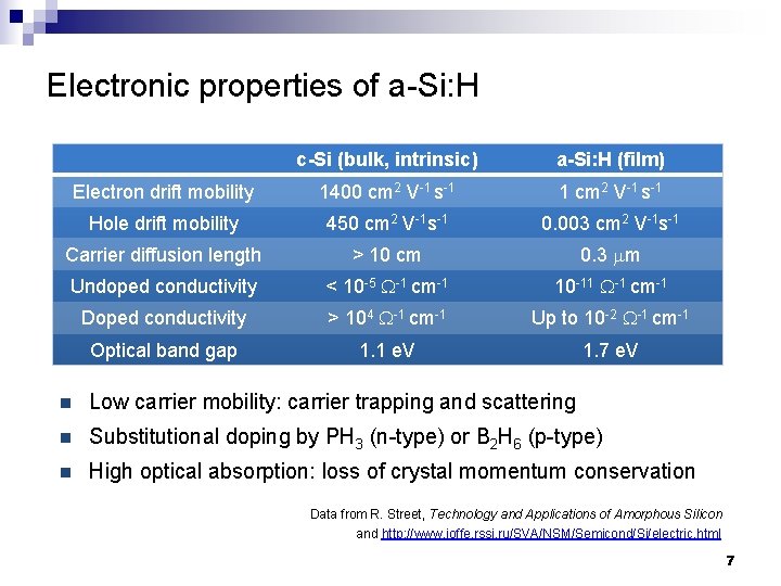
Electronic properties of a-Si: H c-Si (bulk, intrinsic) a-Si: H (film) Electron drift mobility 1400 cm 2 V-1 s-1 1 cm 2 V-1 s-1 Hole drift mobility 450 cm 2 V-1 s-1 0. 003 cm 2 V-1 s-1 Carrier diffusion length > 10 cm 0. 3 mm Undoped conductivity < 10 -5 W-1 cm-1 10 -11 W-1 cm-1 Doped conductivity > 104 W-1 cm-1 Up to 10 -2 W-1 cm-1 Optical band gap 1. 1 e. V 1. 7 e. V n Low carrier mobility: carrier trapping and scattering n Substitutional doping by PH 3 (n-type) or B 2 H 6 (p-type) n High optical absorption: loss of crystal momentum conservation Data from R. Street, Technology and Applications of Amorphous Silicon and http: //www. ioffe. rssi. ru/SVA/NSM/Semicond/Si/electric. html 7

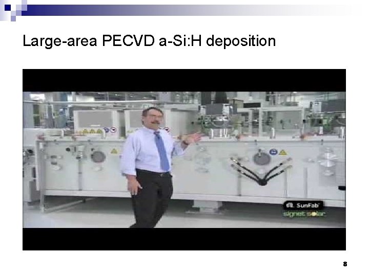
Large-area PECVD a-Si: H deposition 8

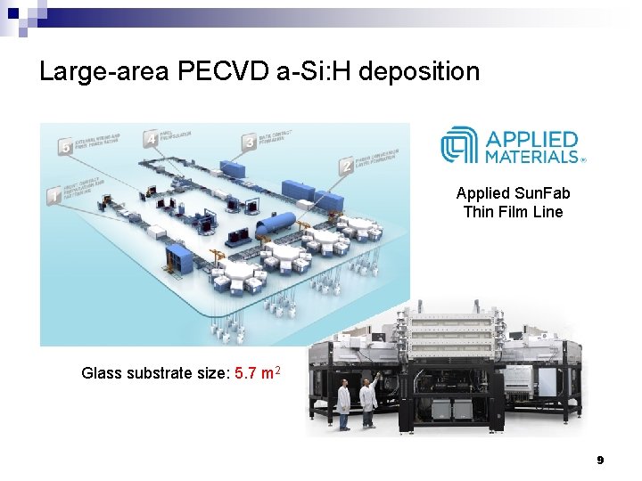
Large-area PECVD a-Si: H deposition Applied Sun. Fab Thin Film Line Glass substrate size: 5. 7 m 2 9

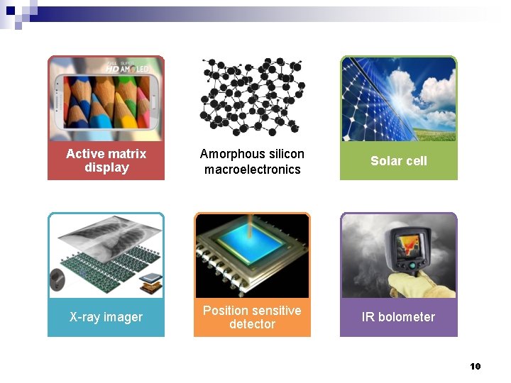
Active matrix display Amorphous silicon macroelectronics Solar cell X-ray imager Position sensitive detector IR bolometer 10

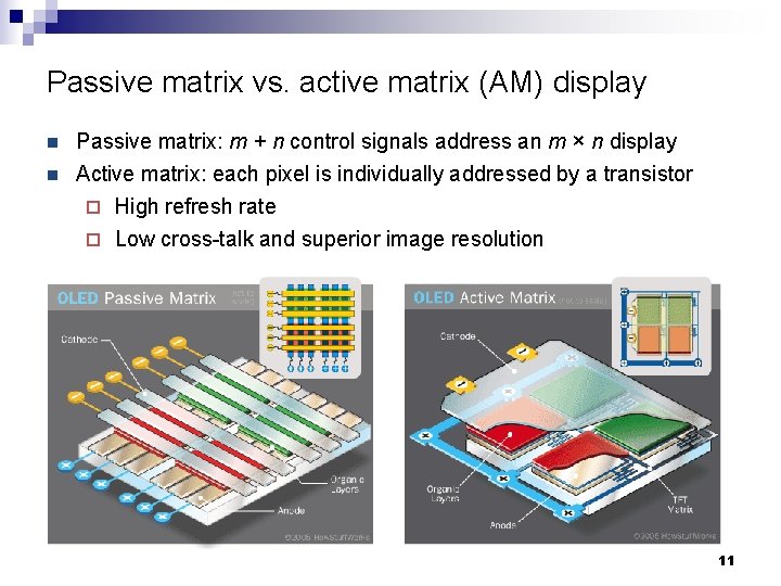
Passive matrix vs. active matrix (AM) display n n Passive matrix: m + n control signals address an m × n display Active matrix: each pixel is individually addressed by a transistor High refresh rate ¨ Low cross-talk and superior image resolution ¨ 11

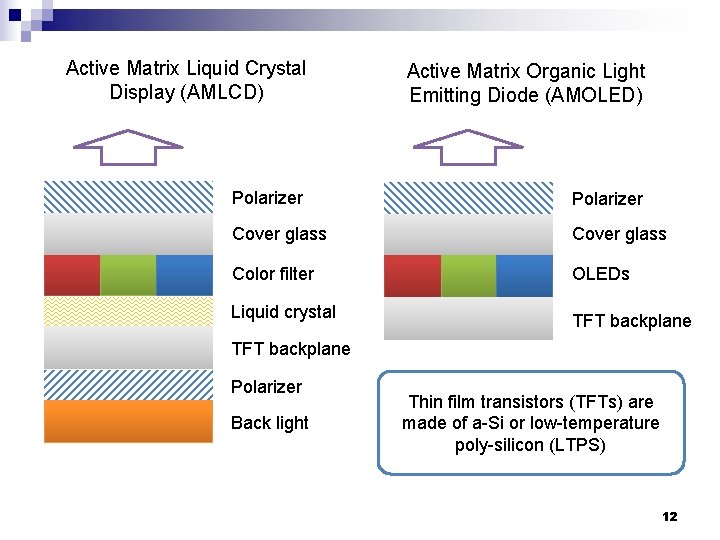
Active Matrix Liquid Crystal Display (AMLCD) Active Matrix Organic Light Emitting Diode (AMOLED) Polarizer Cover glass Color filter OLEDs Liquid crystal TFT backplane Polarizer Back light Thin film transistors (TFTs) are made of a-Si or low-temperature poly-silicon (LTPS) 12

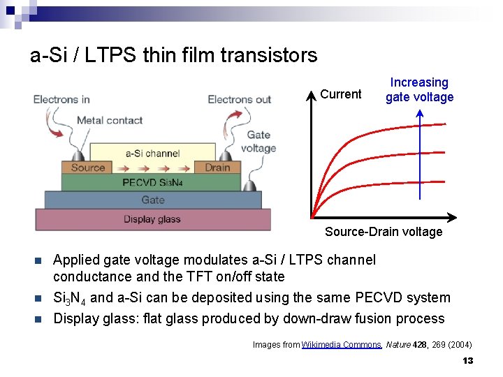
a-Si / LTPS thin film transistors Current Increasing gate voltage AMLCD display under microscope Source-Drain voltage n Applied gate voltage modulates a-Si / LTPS channel conductance and the TFT on/off state n Si 3 N 4 and a-Si can be deposited using the same PECVD system Display glass: flat glass produced by down-draw fusion process n Images from Wikimedia Commons, Nature 428, 269 (2004) 13

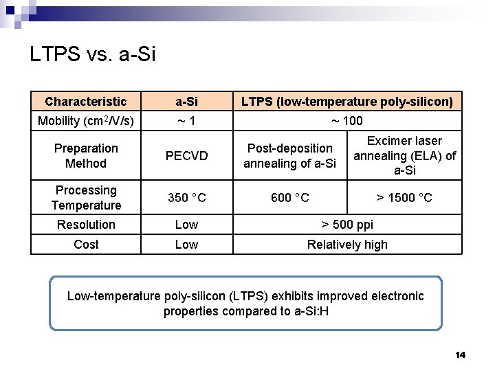
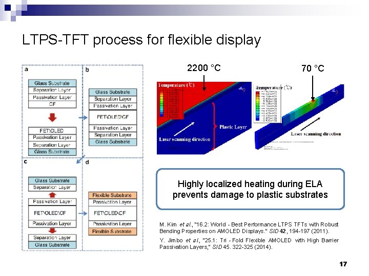
LTPS vs. a-Si Characteristic a-Si LTPS (low-temperature poly-silicon) Mobility (cm 2/V/s) ~1 ~ 100 PECVD Post-deposition annealing of a-Si Excimer laser annealing (ELA) of a-Si Processing Temperature 350 °C 600 °C > 1500 °C Resolution Low > 500 ppi Cost Low Relatively high Preparation Method Low-temperature poly-silicon (LTPS) exhibits improved electronic properties compared to a-Si: H 14

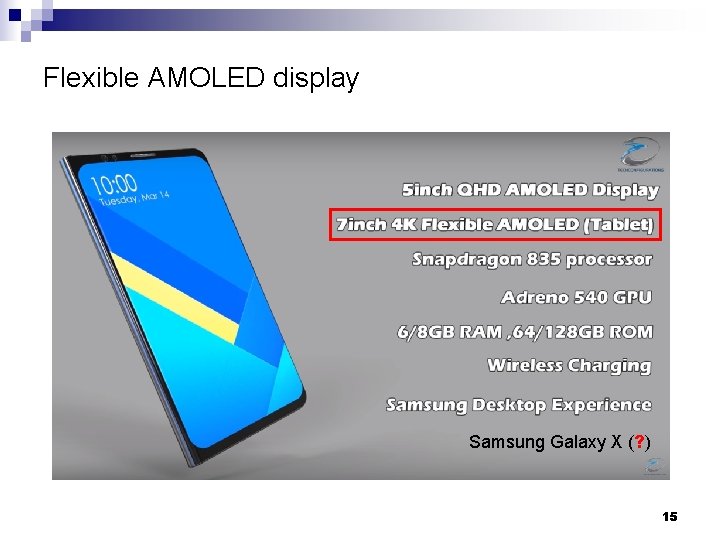
Flexible AMOLED display Samsung Galaxy X (? ) 15

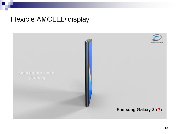
Flexible AMOLED display Samsung Galaxy X (? ) 16

LTPS-TFT process for flexible display 2200 °C 70 °C Highly localized heating during ELA prevents damage to plastic substrates M. Kim et al. , "16. 2: World‐Best Performance LTPS TFTs with Robust Bending Properties on AMOLED Displays. " SID 42, 194 -197 (2011). Y. Jimbo et al. , "25. 1: Tri‐Fold Flexible AMOLED with High Barrier Passivation Layers, " SID 45. 322 -325 (2014). 17

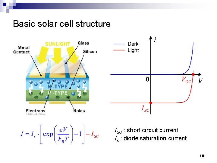
Basic solar cell structure I 0 V ISC : short circuit current Is : diode saturation current 18

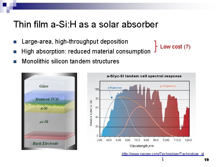
Thin film a-Si: H as a solar absorber n Large-area, high-throughput deposition n High absorption: reduced material consumption n Monolithic silicon tandem structures Low cost (? ) http: //www. nexpw. com/Technology_st t 19

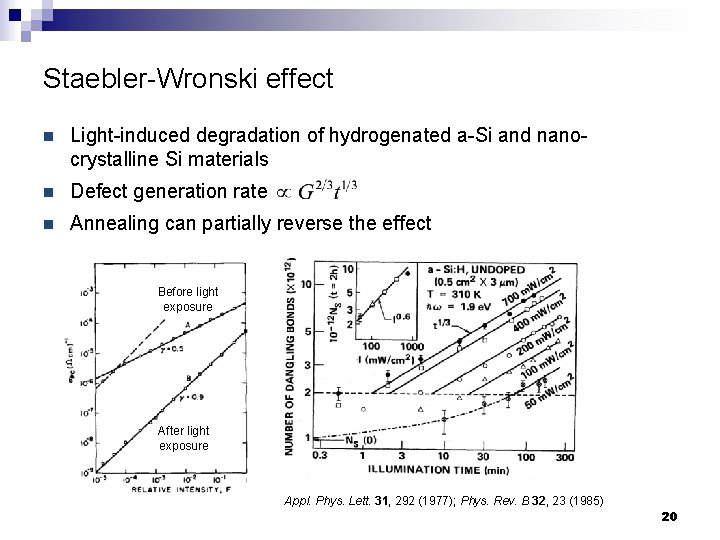
Staebler-Wronski effect n Light-induced degradation of hydrogenated a-Si and nanocrystalline Si materials n Defect generation rate n Annealing can partially reverse the effect Before light exposure After light exposure Appl. Phys. Lett. 31, 292 (1977); Phys. Rev. B 32, 23 (1985) 20

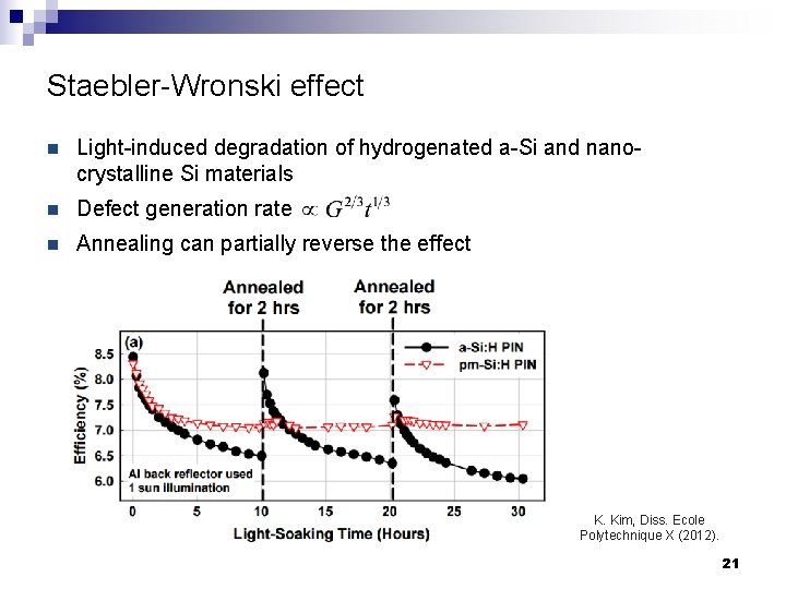
Staebler-Wronski effect n Light-induced degradation of hydrogenated a-Si and nanocrystalline Si materials n Defect generation rate n Annealing can partially reverse the effect K. Kim, Diss. Ecole Polytechnique X (2012). 21

22

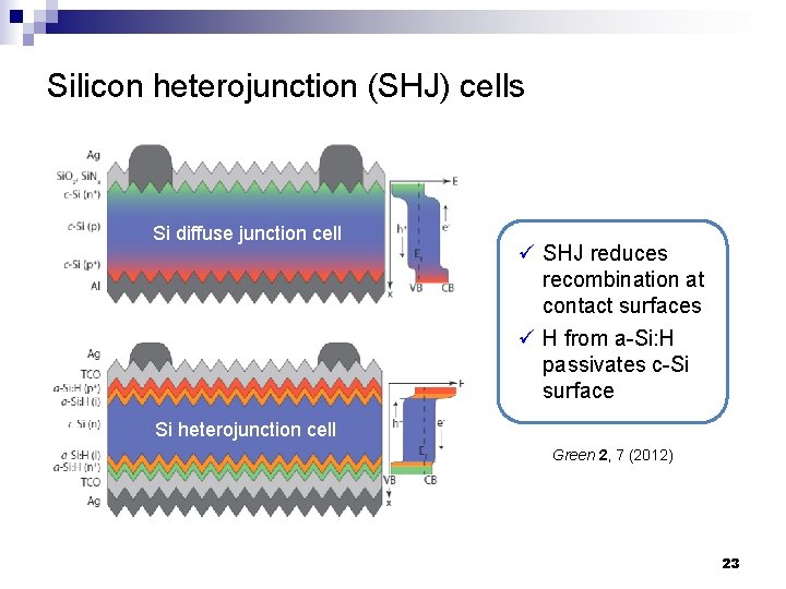
Silicon heterojunction (SHJ) cells Si diffuse junction cell ü SHJ reduces recombination at contact surfaces ü H from a-Si: H passivates c-Si surface Si heterojunction cell Green 2, 7 (2012) 23

Summary n n Basic properties of a-Si and a-Si: H ¨ Dangling bonds and hydrogenation ¨ Electronic properties: Fermi level pinning, factors affecting drift mobility and optical absorption Active matrix display based on TFTs ¨ n Comparison of a-Si and LTPS a-Si solar cells ¨ Staebler-Wronski effect 24

Further Readings n n Springer Handbook of Electronic and Photonic Materials ¨ Ch. 25: Amorphous Semiconductors: Structural, Optical, and Electrical Properties ¨ Ch. 26: Amorphous and Microcrystalline Silicon ¨ Springer Link (paste link to a browser window) Technology and Applications of Amorphous Silicon ¨ R. A. Street, Springer (2000) ¨ Springer Link (paste link to a browser window) 25