MIPS processor continued In Class Exercise Question Show

- Slides: 18

MIPS processor continued

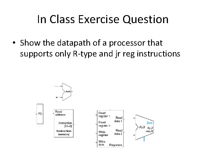
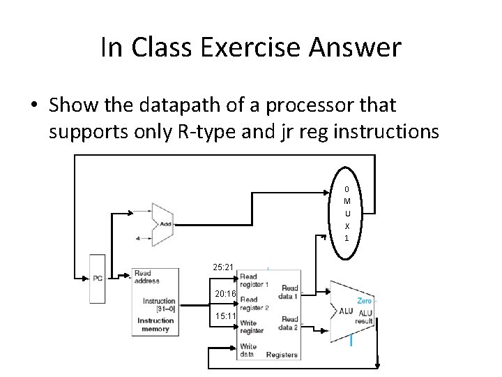
In Class Exercise Question • Show the datapath of a processor that supports only R-type and jr reg instructions

In Class Exercise Answer • Show the datapath of a processor that supports only R-type and jr reg instructions 0 M U X 1 25: 21 20: 16 15: 11

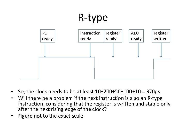
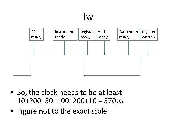
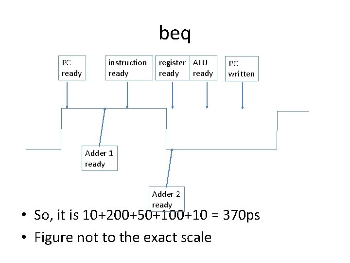
Performance • Assume that – – – – Memory access: 200 ps ALU and adders: 100 ps Register file read: 50 ps Register file write: 10 ps (the clk-to-q delay) PC update: 10 ps (the clk-to-q delay) The setup time of DFFs: 10 ps Other parts do not have delay • How fast is – – An R-type instruction? A lw instruction? A sw instruction? A beq instruction? • Need to find the critical path – the longest path

R-type PC ready instruction ready register ready ALU ready register written • So, the clock needs to be at least 10+200+50+10 = 370 ps • Will there be a problem if the next instruction is also an R-type instruction, considering that the register is written and stable only after the next rising edge of the clock? • Figure not to the exact scale

lw PC ready instruction ready register ALU ready Data mem register ready written • So, the clock needs to be at least 10+200+50+100+200+10 = 570 ps • Figure not to the exact scale

beq PC ready instruction ready register ALU ready PC written Adder 1 ready Adder 2 ready • So, it is 10+200+50+10 = 370 ps • Figure not to the exact scale

Clock cycle • So, how long should the clock cycle be? • Is it efficient?

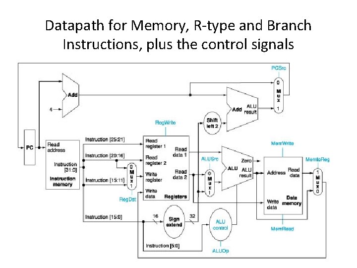
Control Signals • Control signals include ALUCtrl and the signals to control the 2 -1 selectors • They are generated according to the current instruction, using the opcode [31 -27] and the funct [5 -0] field in the instruction.

Datapath for Memory, R-type and Branch Instructions, plus the control signals

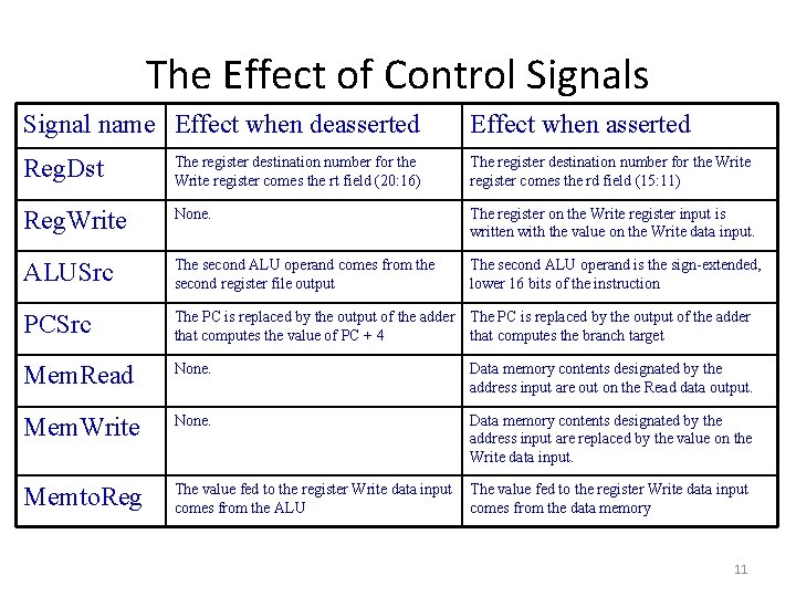
The Effect of Control Signals Signal name Effect when deasserted Effect when asserted Reg. Dst The register destination number for the Write register comes the rt field (20: 16) The register destination number for the Write register comes the rd field (15: 11) Reg. Write None. The register on the Write register input is written with the value on the Write data input. ALUSrc The second ALU operand comes from the second register file output The second ALU operand is the sign-extended, lower 16 bits of the instruction PCSrc The PC is replaced by the output of the adder that computes the value of PC + 4 that computes the branch target Mem. Read None. Data memory contents designated by the address input are out on the Read data output. Mem. Write None. Data memory contents designated by the address input are replaced by the value on the Write data input. Memto. Reg The value fed to the register Write data input comes from the ALU The value fed to the register Write data input comes from the data memory 11

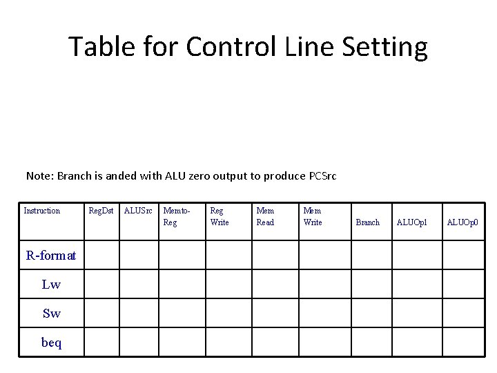
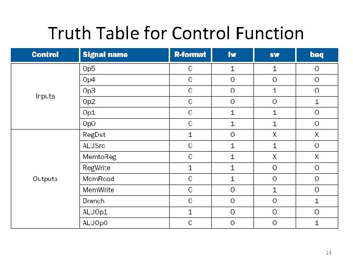
Table for Control Line Setting Note: Branch is anded with ALU zero output to produce PCSrc Instruction R-format Lw Sw beq Reg. Dst ALUSrc Memto. Reg Write Mem Read Mem Write Branch ALUOp 1 ALUOp 0

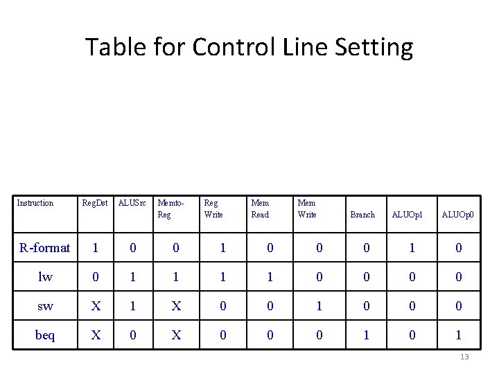
Table for Control Line Setting Instruction Reg. Dst ALUSrc Memto. Reg Write Mem Read Mem Write Branch ALUOp 1 ALUOp 0 R-format 1 0 0 0 1 0 lw 0 1 1 0 0 sw X 1 X 0 0 1 0 0 0 beq X 0 0 0 1 13

Truth Table for Control Function 14

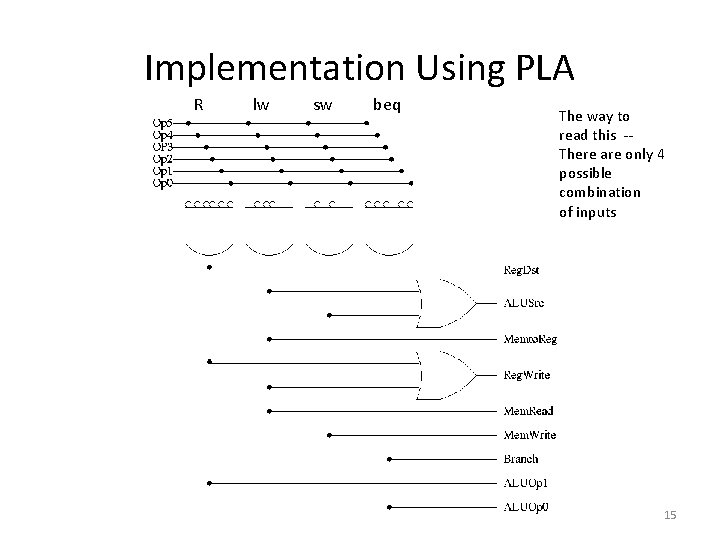
Implementation Using PLA R lw sw beq The way to read this -There are only 4 possible combination of inputs 15

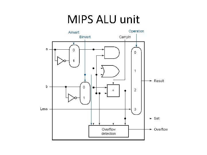
MIPS ALU unit

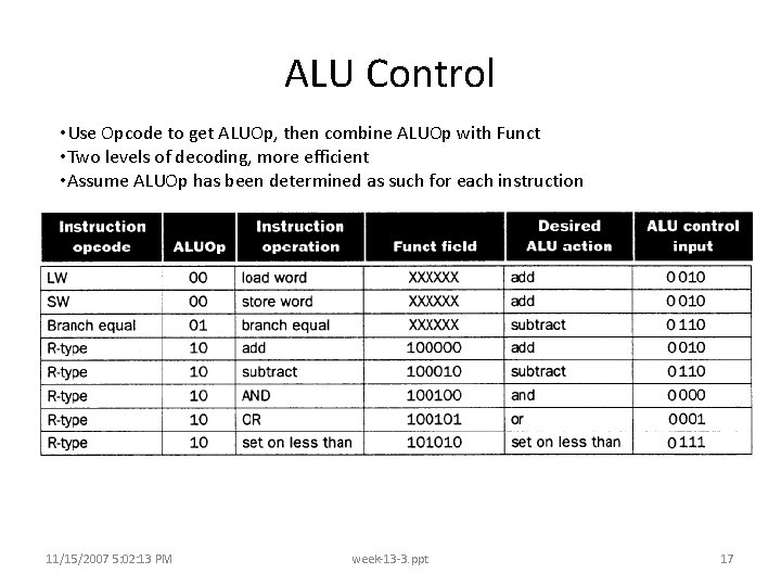
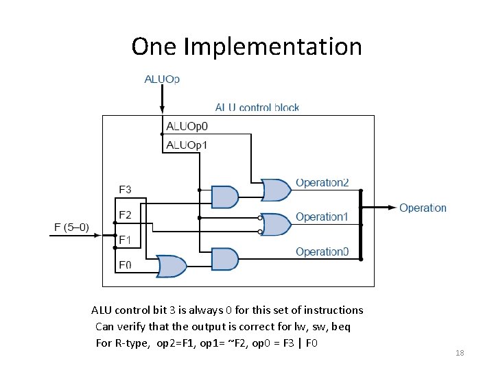
ALU Control • Use Opcode to get ALUOp, then combine ALUOp with Funct • Two levels of decoding, more efficient • Assume ALUOp has been determined as such for each instruction 11/15/2007 5: 02: 13 PM week-13 -3. ppt 17

One Implementation ALU control bit 3 is always 0 for this set of instructions Can verify that the output is correct for lw, sw, beq For R-type, op 2=F 1, op 1= ~F 2, op 0 = F 3 | F 0 18