MINIATURIZATION CHALLENGES IN OPTICAL SENSING Leti Photonics Workshop
- Slides: 11

MINIATURIZATION CHALLENGES IN OPTICAL SENSING Leti Photonics Workshop - 31/01/2018 | Sergio Nicoletti

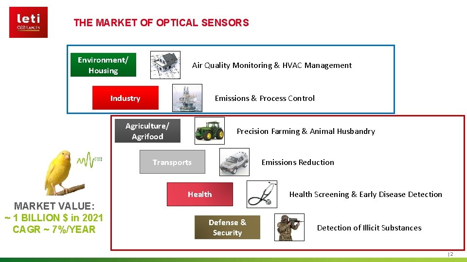
THE MARKET OF OPTICAL SENSORS Environment/ Housing Air Quality Monitoring & HVAC Management Industry Emissions & Process Control Agriculture/ Agrifood Precision Farming & Animal Husbandry Transports Emissions Reduction Health MARKET VALUE: ~ 1 BILLION $ in 2021 CAGR ~ 7%/YEAR Defense & Security Health Screening & Early Disease Detection of Illicit Substances | 2

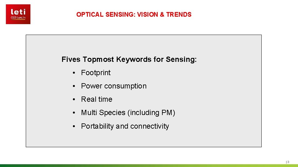
OPTICAL SENSING: VISION & TRENDS • e. Lichens: Personalized Air Quality Fives. Labs: Topmost Keywords for Sensing: • Plume The first smart air quality tracker • Footprint • Sense. Air: Make sense of air • Power consumption • mir. Sense: Sensing the world to make it a better place • Real time • Multi Species (including PM) • Aryballe: Imagine if you could record a smell • Portability and connectivity • Vaisala: Reliable environmental observations for better decision making, safety and efficiency. | 3

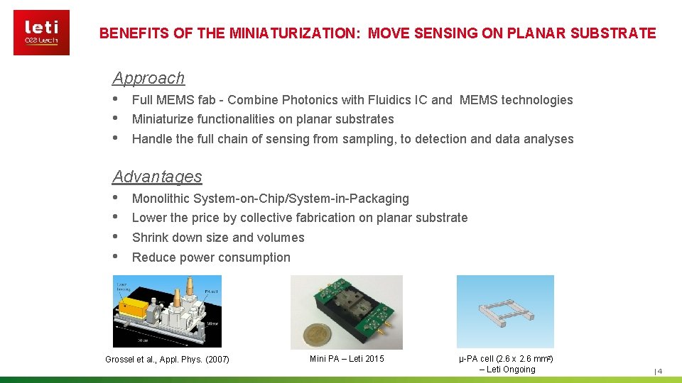
BENEFITS OF THE MINIATURIZATION: MOVE SENSING ON PLANAR SUBSTRATE Approach • Full MEMS fab - Combine Photonics with Fluidics IC and MEMS technologies • Miniaturize functionalities on planar substrates • Handle the full chain of sensing from sampling, to detection and data analyses Advantages • Monolithic System-on-Chip/System-in-Packaging • Lower the price by collective fabrication on planar substrate • Shrink down size and volumes • Reduce power consumption Grossel et al. , Appl. Phys. (2007) Mini PA – Leti 2015 µ-PA cell (2. 6 x 2. 6 mm 2) – Leti Ongoing | 4

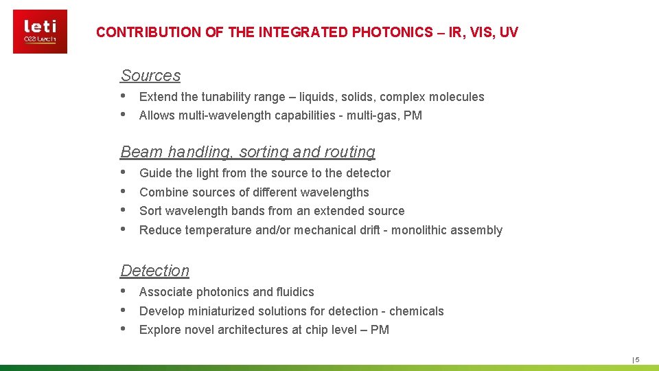
CONTRIBUTION OF THE INTEGRATED PHOTONICS – IR, VIS, UV Sources • Extend the tunability range – liquids, solids, complex molecules • Allows multi-wavelength capabilities - multi-gas, PM Beam handling, sorting and routing • Guide the light from the source to the detector • Combine sources of different wavelengths • Sort wavelength bands from an extended source • Reduce temperature and/or mechanical drift - monolithic assembly Detection • Associate photonics and fluidics • Develop miniaturized solutions for detection - chemicals • Explore novel architectures at chip level – PM | 5

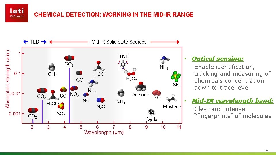
CHEMICAL DETECTION: WORKING IN THE MID-IR RANGE • Optical sensing: Enable identification, tracking and measuring of chemicals concentration down to trace level • Mid-IR wavelength band: Clear and intense “fingerprints” of molecules | 6

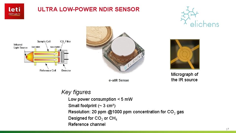
ULTRA LOW-POWER NDIR SENSOR Micrograph of the IR source Key figures Low power consumption < 5 m. W Small footprint (~ 3 cm²) Resolution: 20 ppm @1000 ppm concentration for CO 2 gas Designed for CO 2 or CH 4 Reference channel | 7

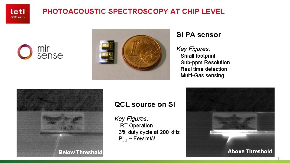
PHOTOACOUSTIC SPECTROSCOPY AT CHIP LEVEL Si PA sensor Key Figures: Small footprint Sub-ppm Resolution Real time detection Multi-Gas sensing QCL source on Si Key Figures: RT Operation 3% duty cycle at 200 k. Hz Pout ~ Few m. W Below Threshold Above Threshold | 8

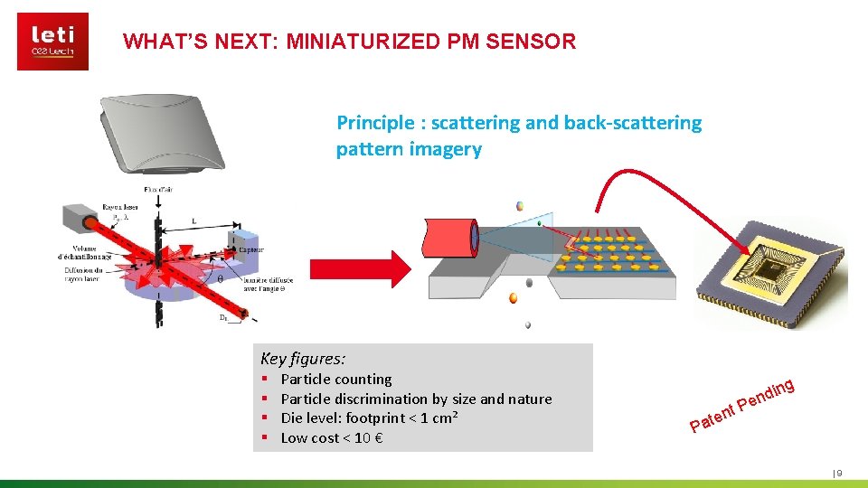
WHAT’S NEXT: MINIATURIZED PM SENSOR Principle : scattering and back-scattering pattern imagery Fluidic channel with particules Key figures: § § Particle counting Particle discrimination by size and nature Die level: footprint < 1 cm² Low cost < 10 € P t P n ate ng i end | 9

Summary Our trusts: Ø Miniaturization to drive cost and power consumption reductions Ø Unique approach combining MEMS and Photonics technologies Our offer: Ø From concept devices to So. C/Si. P validation; Ø From Proof Of Concept to Prototyping & Industrialization | 10

Meet Leti experts at Booth #431 French Pavilion South Hall Leti, technology research institute Commissariat à l’énergie atomique et aux énergies alternatives Minatec Campus | 17 rue des Martyrs | 38054 Grenoble Cedex | France www. leti. fr