Microwave Filter Design By Professor Syed Idris Syed
Microwave Filter Design By Professor Syed Idris Syed Hassan Sch of Elect. & Electron Engineering Campus USM Nibong Tebal 14300 SPS Penang
Contents 1. Composite filter 2. LC ladder filter 3. Microwave filter 2
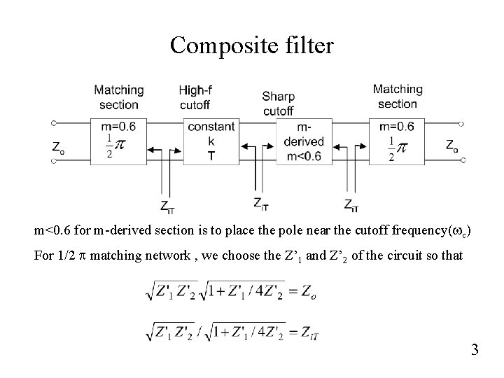
Composite filter m<0. 6 for m-derived section is to place the pole near the cutoff frequency(wc) For 1/2 p matching network , we choose the Z’ 1 and Z’ 2 of the circuit so that 3
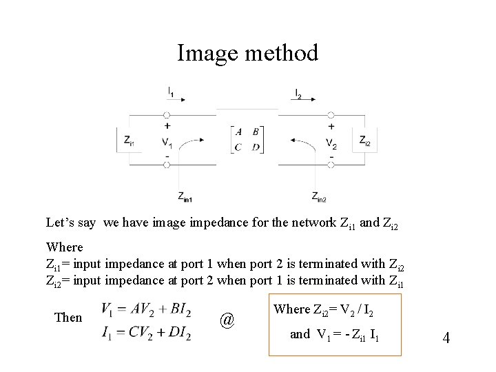
Image method Let’s say we have image impedance for the network Zi 1 and Zi 2 Where Zi 1= input impedance at port 1 when port 2 is terminated with Zi 2= input impedance at port 2 when port 1 is terminated with Zi 1 Then @ Where Zi 2= V 2 / I 2 and V 1 = - Zi 1 I 1 4
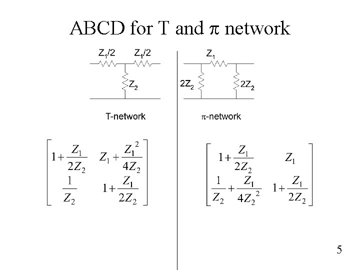
ABCD for T and p network 5
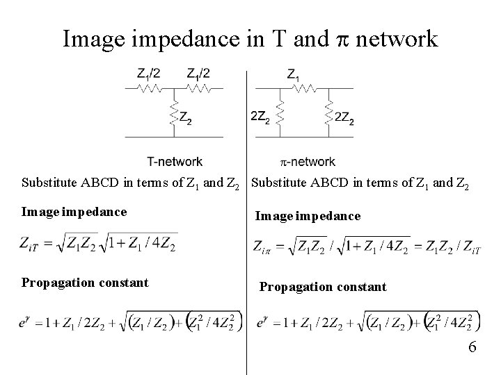
Image impedance in T and p network Substitute ABCD in terms of Z 1 and Z 2 Image impedance Propagation constant 6
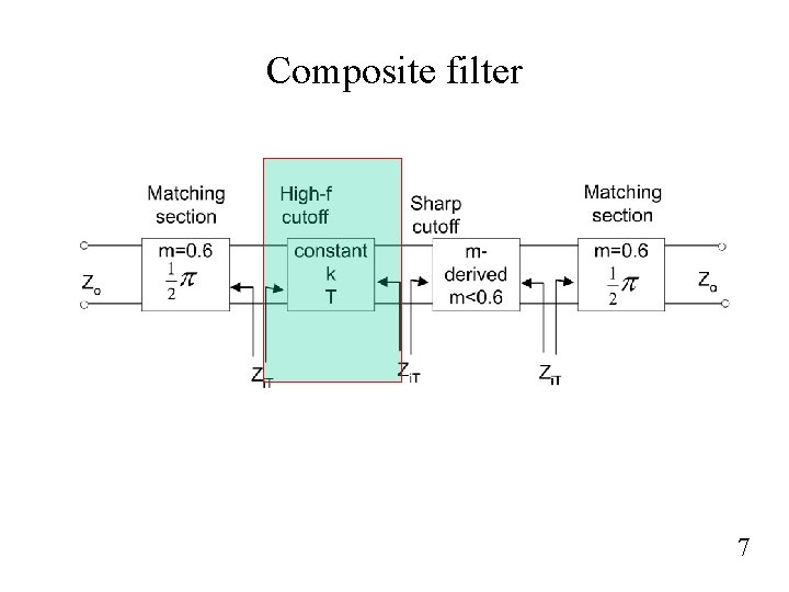
Composite filter 7
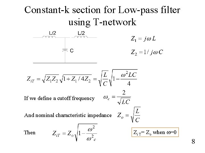
Constant-k section for Low-pass filter using T-network If we define a cutoff frequency And nominal characteristic impedance Then Zi T= Zo when w=0 8
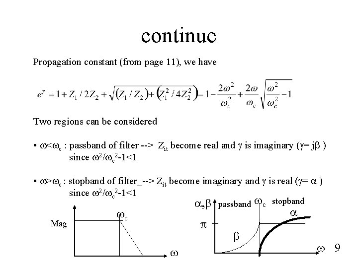
continue Propagation constant (from page 11), we have Two regions can be considered • w<wc : passband of filter --> Zit become real and g is imaginary (g= jb ) since w 2/wc 2 -1<1 • w>wc : stopband of filter_--> Zit become imaginary and g is real (g= a ) since w 2/wc 2 -1<1 Mag a, b wc p w passband b wc stopband a w 9
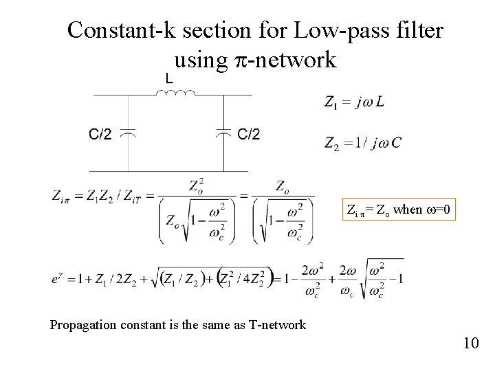
Constant-k section for Low-pass filter using p-network Zi p= Zo when w=0 Propagation constant is the same as T-network 10
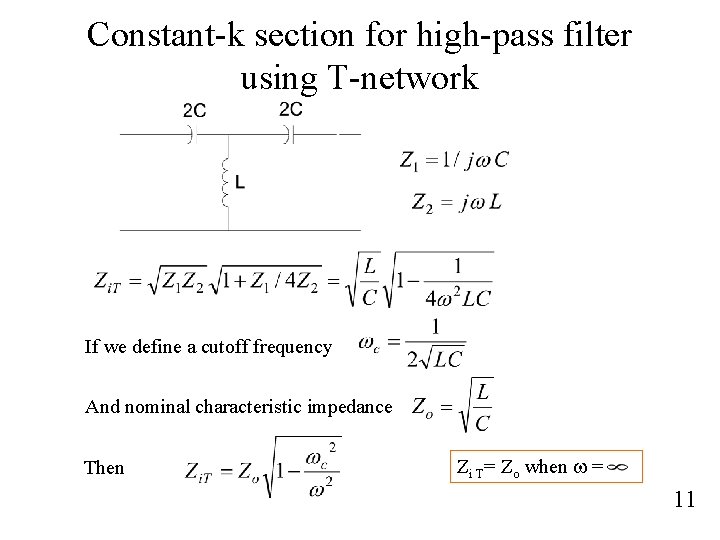
Constant-k section for high-pass filter using T-network If we define a cutoff frequency And nominal characteristic impedance Then Zi T= Zo when w = 11

Constant-k section for high-pass filter using p-network Zi p= Zo when w= Propagation constant is the same for both T and p-network 12
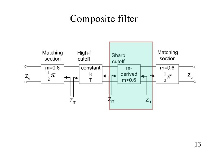
Composite filter 13
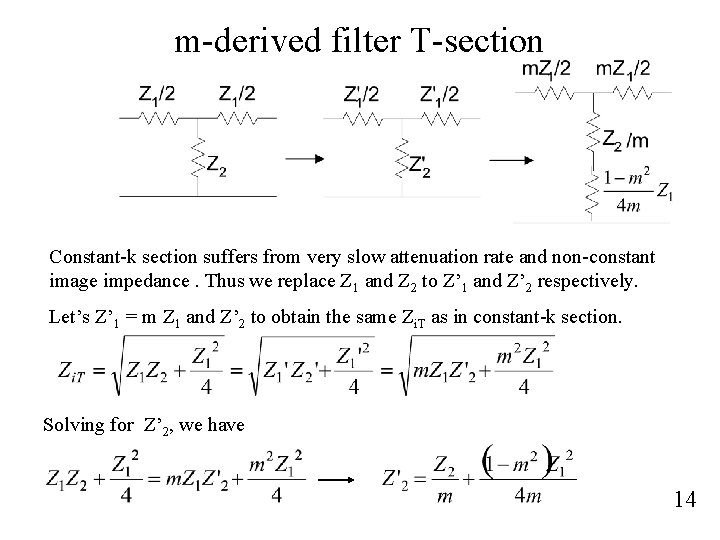
m-derived filter T-section Constant-k section suffers from very slow attenuation rate and non-constant image impedance. Thus we replace Z 1 and Z 2 to Z’ 1 and Z’ 2 respectively. Let’s Z’ 1 = m Z 1 and Z’ 2 to obtain the same Zi. T as in constant-k section. Solving for Z’ 2, we have 14

Low -pass m-derived T-section For constant-k section and Propagation constant where 15
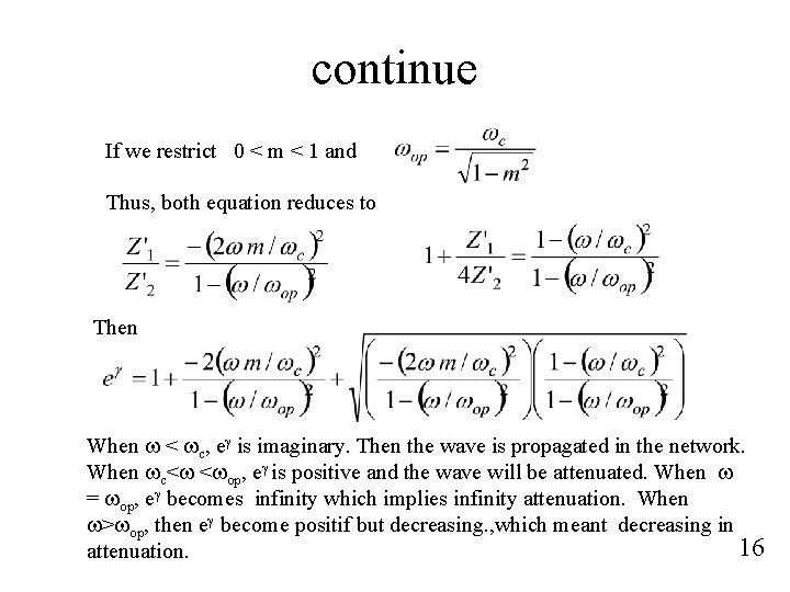
continue If we restrict 0 < m < 1 and Thus, both equation reduces to Then When w < wc, eg is imaginary. Then the wave is propagated in the network. When wc<w <wop, eg is positive and the wave will be attenuated. When w = wop, eg becomes infinity which implies infinity attenuation. When w>wop, then eg become positif but decreasing. , which meant decreasing in 16 attenuation.
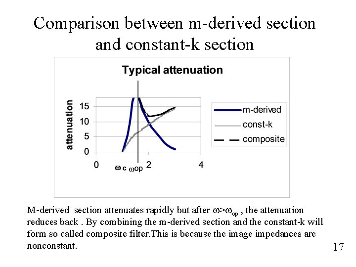
Comparison between m-derived section and constant-k section M-derived section attenuates rapidly but after w>wop , the attenuation reduces back. By combining the m-derived section and the constant-k will form so called composite filter. This is because the image impedances are nonconstant. 17
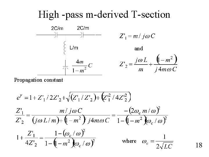
High -pass m-derived T-section and Propagation constant where 18
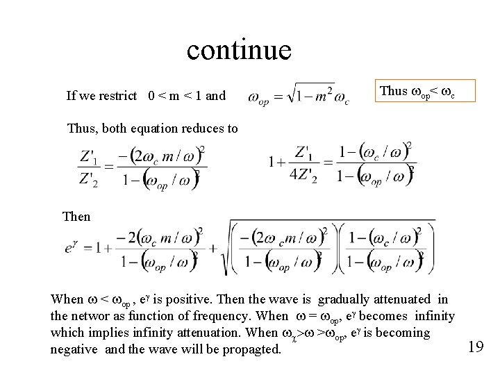
continue If we restrict 0 < m < 1 and Thus wop< wc Thus, both equation reduces to Then When w < wop , eg is positive. Then the wave is gradually attenuated in the networ as function of frequency. When w = wop, eg becomes infinity which implies infinity attenuation. When wc>w >wop, eg is becoming negative and the wave will be propagted. 19
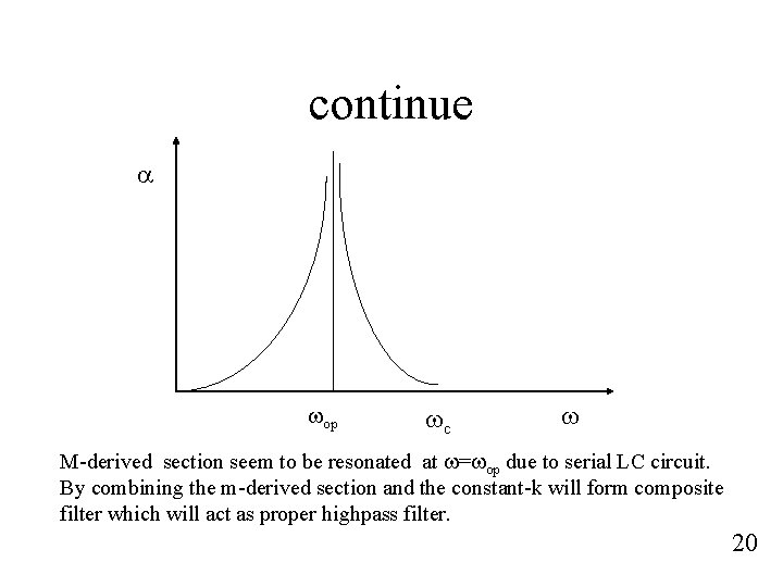
continue a wop wc w M-derived section seem to be resonated at w=wop due to serial LC circuit. By combining the m-derived section and the constant-k will form composite filter which will act as proper highpass filter. 20
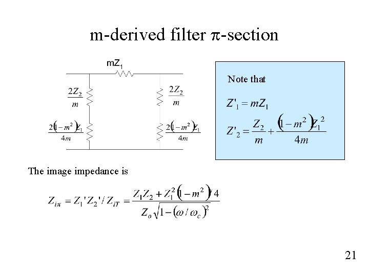
m-derived filter p-section Note that The image impedance is 21
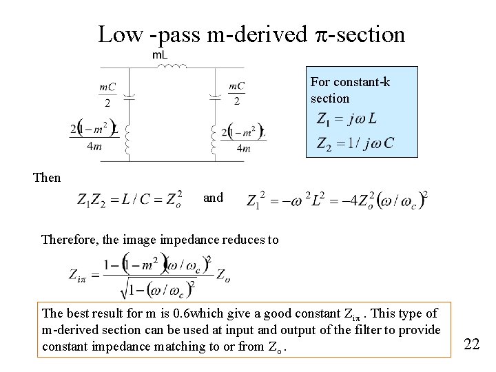
Low -pass m-derived p-section For constant-k section Then and Therefore, the image impedance reduces to The best result for m is 0. 6 which give a good constant Zip. This type of m-derived section can be used at input and output of the filter to provide constant impedance matching to or from Zo. 22
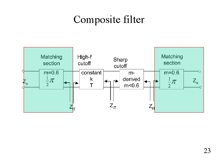
Composite filter 23
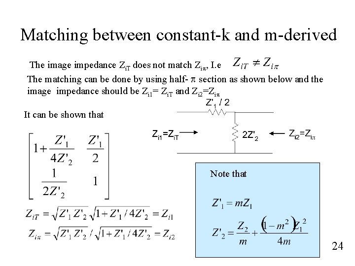
Matching between constant-k and m-derived The image impedance Zi. T does not match Zip, I. e The matching can be done by using half- p section as shown below and the image impedance should be Zi 1= Zi. T and Zi 2=Zip It can be shown that Note that 24

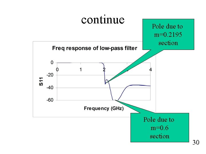
Example #1 Design a low-pass composite filter with cutoff frequency of 2 GHz and impedance of 75 W. Place the infinite attenuation pole at 2. 05 GHz, and plot the frequency response from 0 to 4 GHz. Solution For high f- cutoff constant -k T - section or Rearrange for wc and substituting, we have 25
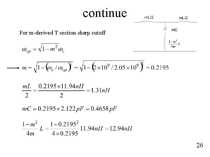
continue For m-derived T section sharp cutoff 26
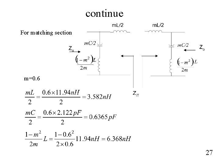
continue For matching section m=0. 6 27

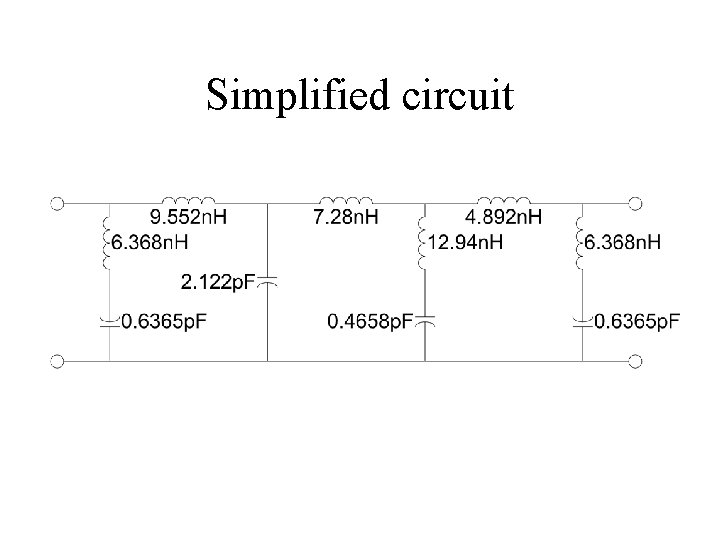
continue A full circuit of the filter 28
Simplified circuit
continue Pole due to m=0. 2195 section Pole due to m=0. 6 section 30
N-section LC ladder circuit (low-pass filter prototypes) Prototype beginning with serial element Prototype beginning with shunt element 31
Type of responses for n-section prototype filter • Maximally flat or Butterworth • Equal ripple or Chebyshev • Elliptic function • Linear phase Maximally flat Equal ripple Elliptic Linear phase 32
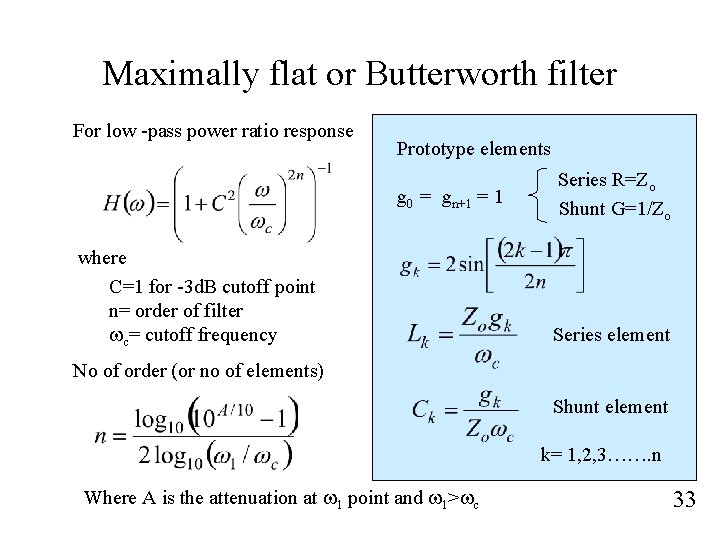
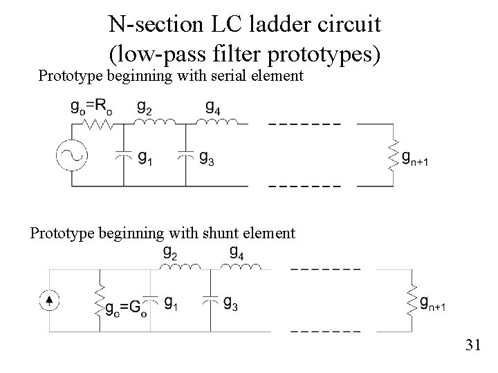
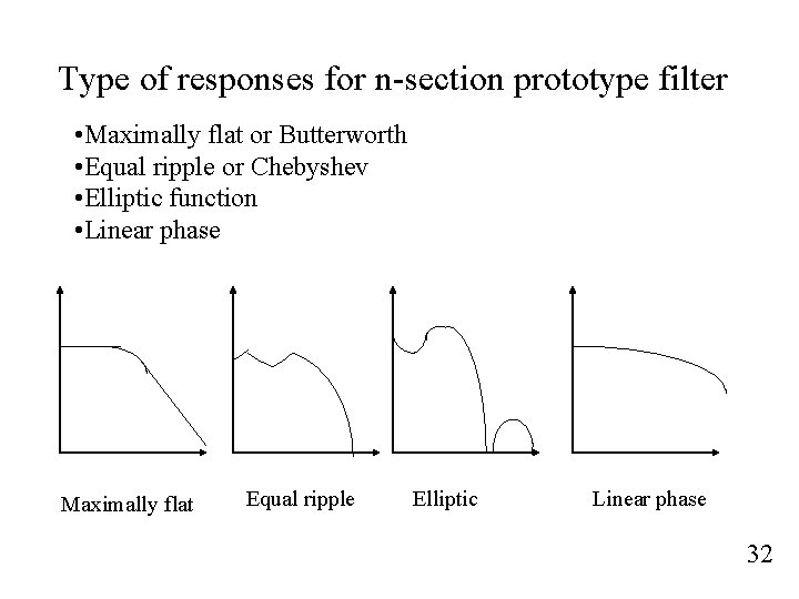
Maximally flat or Butterworth filter For low -pass power ratio response Prototype elements g 0 = gn+1 = 1 where C=1 for -3 d. B cutoff point n= order of filter wc= cutoff frequency Series R=Zo Shunt G=1/Zo Series element No of order (or no of elements) Shunt element k= 1, 2, 3……. n Where A is the attenuation at w 1 point and w 1>wc 33
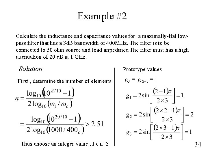
Example #2 Calculate the inductance and capacitance values for a maximally-flat lowpass filter that has a 3 d. B bandwidth of 400 MHz. The filter is to be connected to 50 ohm source and load impedance. The filter must has a high attenuation of 20 d. B at 1 GHz. Solution First , determine the number of elements Thus choose an integer value , I. e n=3 Prototype values g 0 = g 3+1 = 1 34
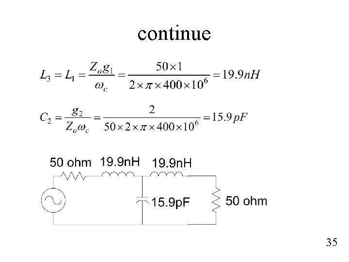
continue 35
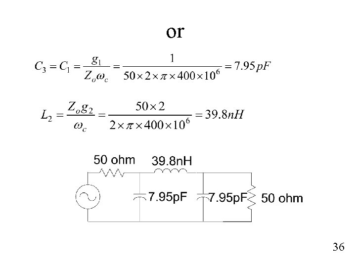
or 36
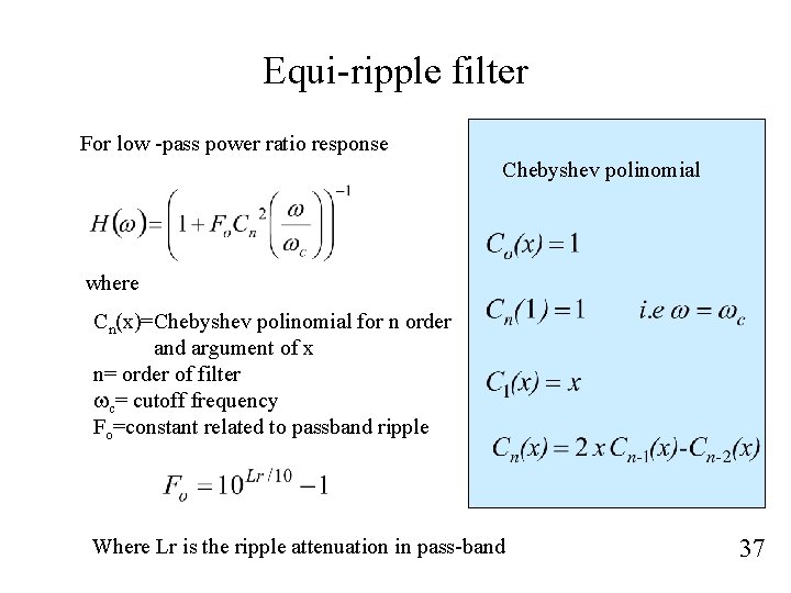
Equi-ripple filter For low -pass power ratio response Chebyshev polinomial where Cn(x)=Chebyshev polinomial for n order and argument of x n= order of filter wc= cutoff frequency Fo=constant related to passband ripple Where Lr is the ripple attenuation in pass-band 37
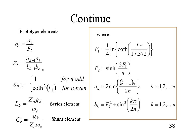
Continue Prototype elements where Series element Shunt element 38
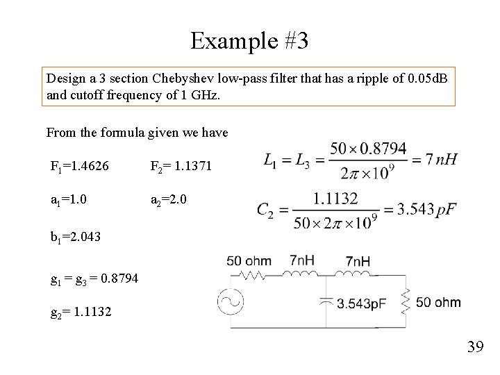
Example #3 Design a 3 section Chebyshev low-pass filter that has a ripple of 0. 05 d. B and cutoff frequency of 1 GHz. From the formula given we have F 1=1. 4626 F 2= 1. 1371 a 1=1. 0 a 2=2. 0 b 1=2. 043 g 1 = g 3 = 0. 8794 g 2= 1. 1132 39
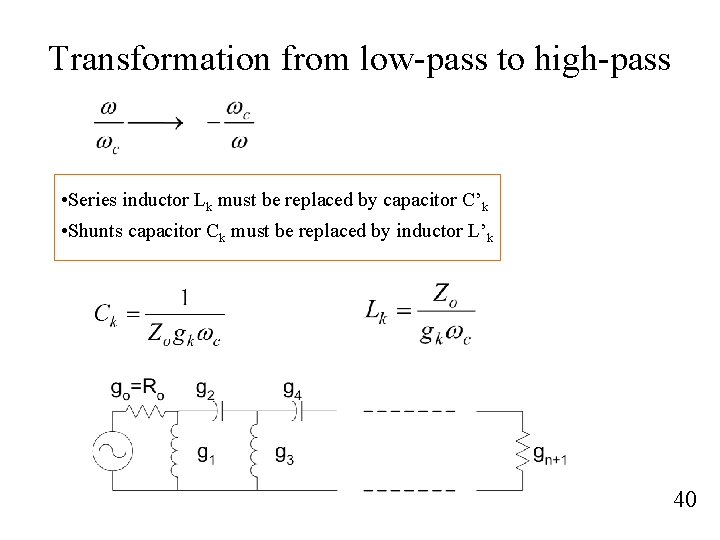
Transformation from low-pass to high-pass • Series inductor Lk must be replaced by capacitor C’k • Shunts capacitor Ck must be replaced by inductor L’k 40
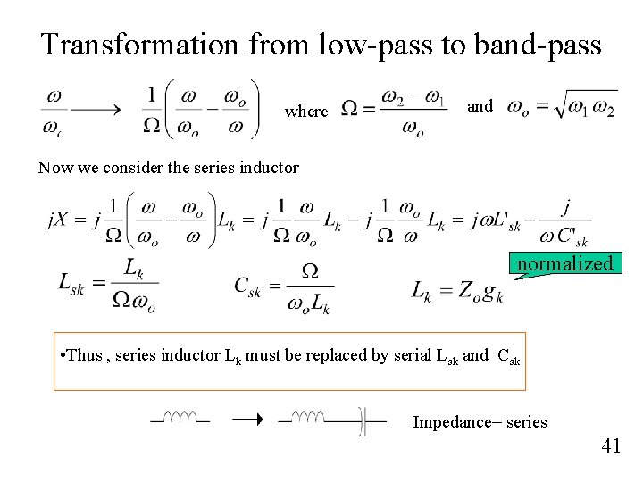
Transformation from low-pass to band-pass where and Now we consider the series inductor normalized • Thus , series inductor Lk must be replaced by serial Lsk and Csk Impedance= series 41
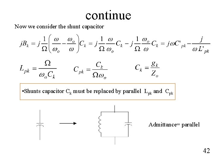
continue Now we consider the shunt capacitor • Shunts capacitor Ck must be replaced by parallel Lpk and Cpk Admittance= parallel 42
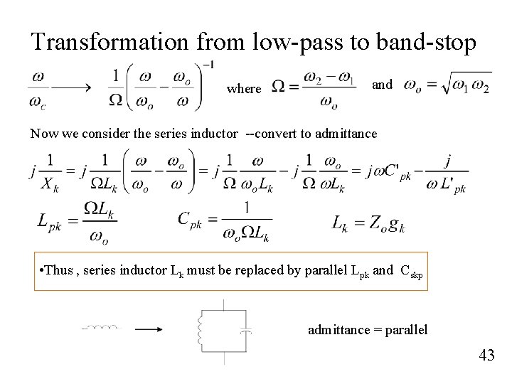
Transformation from low-pass to band-stop where and Now we consider the series inductor --convert to admittance • Thus , series inductor Lk must be replaced by parallel Lpk and Cskp admittance = parallel 43
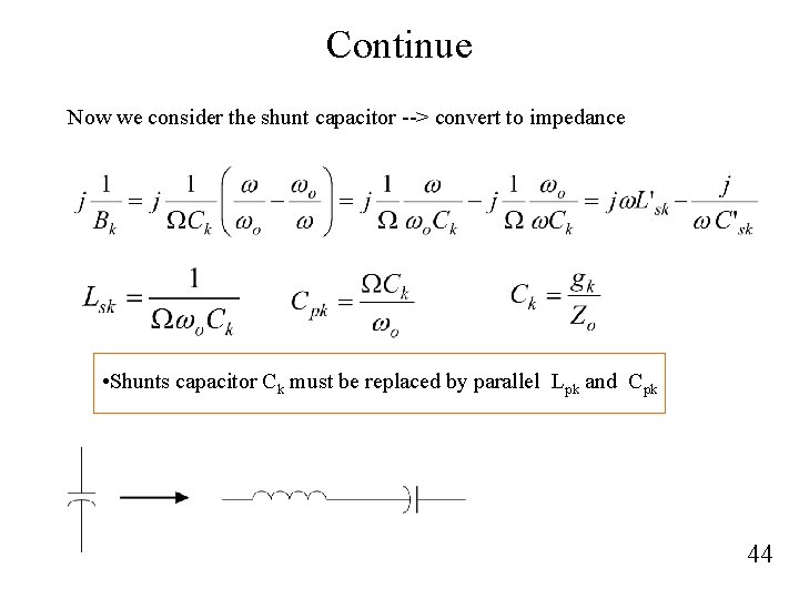
Continue Now we consider the shunt capacitor --> convert to impedance • Shunts capacitor Ck must be replaced by parallel Lpk and Cpk 44
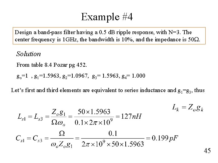
Example #4 Design a band-pass filter having a 0. 5 d. B ripple response, with N=3. The center frequency is 1 GHz, the bandwidth is 10%, and the impedance is 50 W. Solution From table 8. 4 Pozar pg 452. go=1 , g 1=1. 5963, g 2=1. 0967, g 3= 1. 5963, g 4= 1. 000 Let’s first and third elements are equivalent to series inductance and g 1=g 3, thus 45
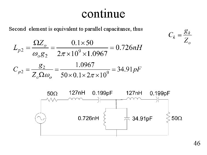
continue Second element is equivalent to parallel capacitance, thus 46
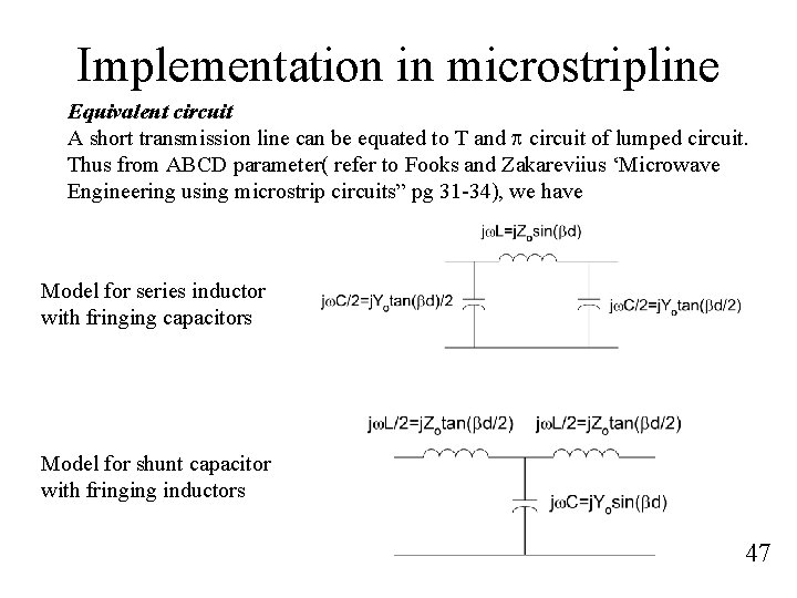
Implementation in microstripline Equivalent circuit A short transmission line can be equated to T and p circuit of lumped circuit. Thus from ABCD parameter( refer to Fooks and Zakareviius ‘Microwave Engineering using microstrip circuits” pg 31 -34), we have Model for series inductor with fringing capacitors Model for shunt capacitor with fringing inductors 47
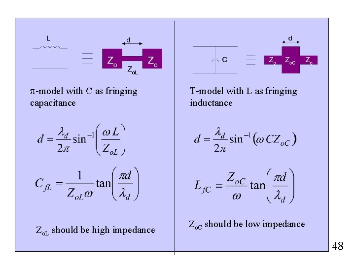
p-model with C as fringing capacitance Zo. L should be high impedance T-model with L as fringing inductance Zo. C should be low impedance 48
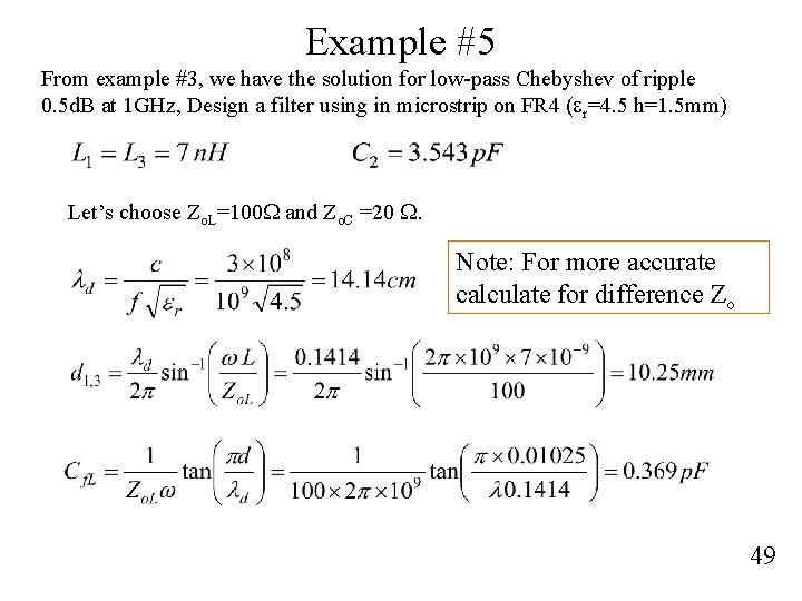
Example #5 From example #3, we have the solution for low-pass Chebyshev of ripple 0. 5 d. B at 1 GHz, Design a filter using in microstrip on FR 4 (er=4. 5 h=1. 5 mm) Let’s choose Zo. L=100 W and Zo. C =20 W. Note: For more accurate calculate for difference Zo 49
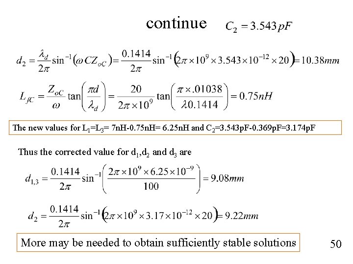
continue The new values for L 1=L 3= 7 n. H-0. 75 n. H= 6. 25 n. H and C 2=3. 543 p. F-0. 369 p. F=3. 174 p. F Thus the corrected value for d 1, d 2 and d 3 are More may be needed to obtain sufficiently stable solutions 50
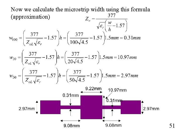
Now we calculate the microstrip width using this formula (approximation) 51
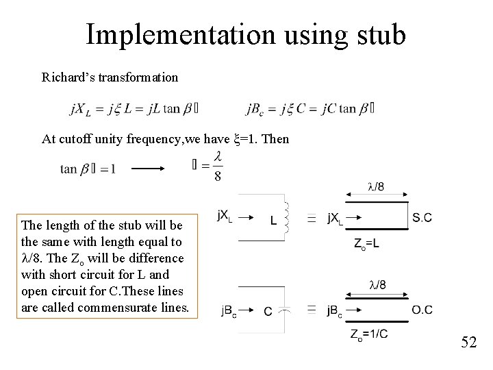
Implementation using stub Richard’s transformation At cutoff unity frequency, we have x=1. Then The length of the stub will be the same with length equal to l/8. The Zo will be difference with short circuit for L and open circuit for C. These lines are called commensurate lines. 52
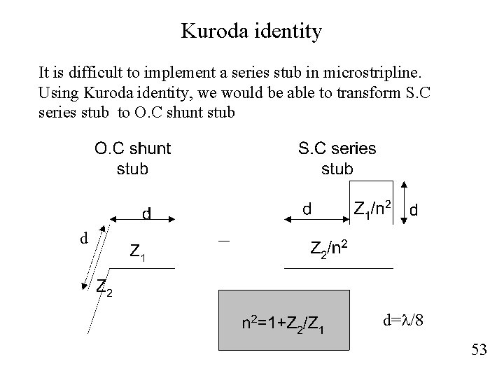
Kuroda identity It is difficult to implement a series stub in microstripline. Using Kuroda identity, we would be able to transform S. C series stub to O. C shunt stub d d=l/8 53
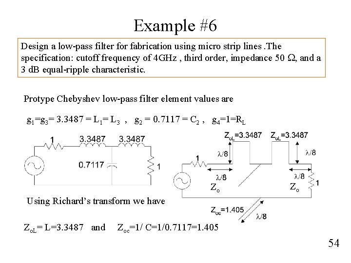
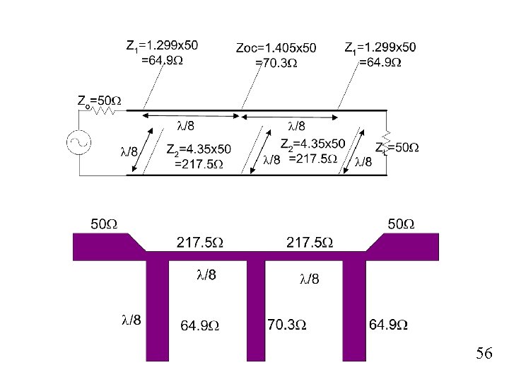
Example #6 Design a low-pass filter for fabrication using micro strip lines. The specification: cutoff frequency of 4 GHz , third order, impedance 50 W, and a 3 d. B equal-ripple characteristic. Protype Chebyshev low-pass filter element values are g 1=g 3= 3. 3487 = L 1= L 3 , g 2 = 0. 7117 = C 2 , g 4=1=RL Zo Zo Using Richard’s transform we have Zo. L= L=3. 3487 and Zoc=1/ C=1/0. 7117=1. 405 54
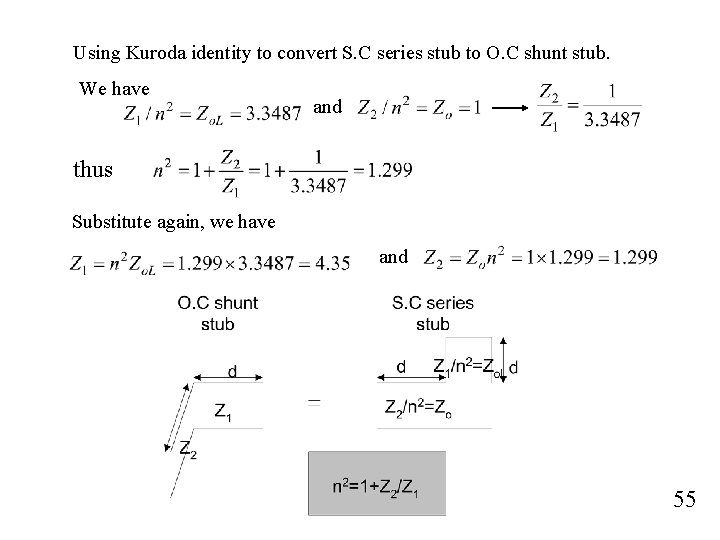
Using Kuroda identity to convert S. C series stub to O. C shunt stub. We have and thus Substitute again, we have and 55
56
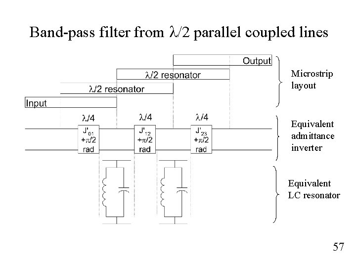
Band-pass filter from l/2 parallel coupled lines Microstrip layout Equivalent admittance inverter Equivalent LC resonator 57
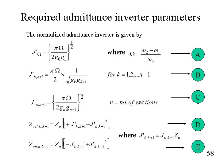
Required admittance inverter parameters The normalized admittance inverter is given by where A B C D where E 58
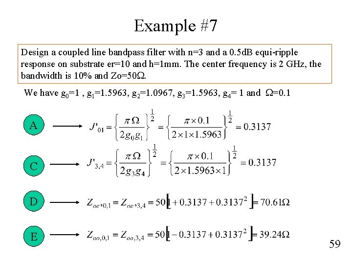
Example #7 Design a coupled line bandpass filter with n=3 and a 0. 5 d. B equi-ripple response on substrate er=10 and h=1 mm. The center frequency is 2 GHz, the bandwidth is 10% and Zo=50 W. We have g 0=1 , g 1=1. 5963, g 2=1. 0967, g 3=1. 5963, g 4= 1 and W=0. 1 A C D E 59
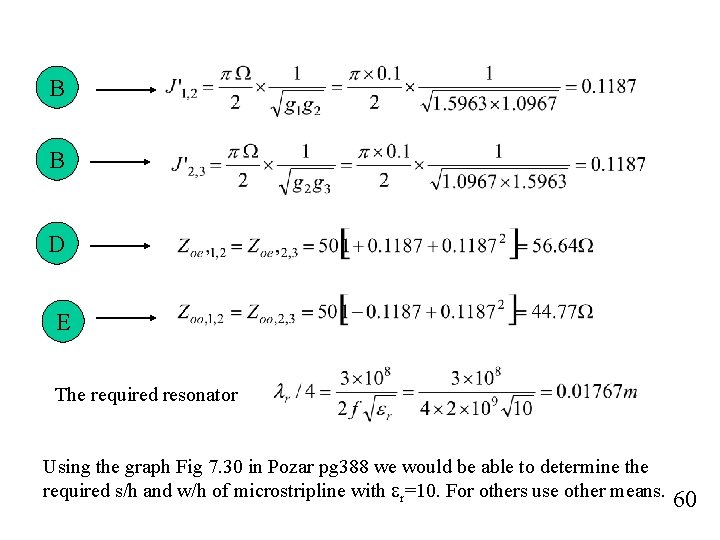
B B D E The required resonator Using the graph Fig 7. 30 in Pozar pg 388 we would be able to determine the required s/h and w/h of microstripline with er=10. For others use other means. 60
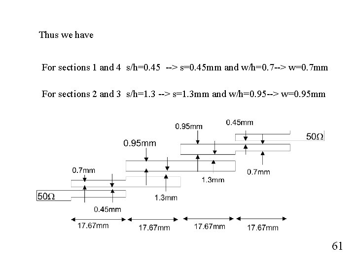
Thus we have For sections 1 and 4 s/h=0. 45 --> s=0. 45 mm and w/h=0. 7 --> w=0. 7 mm For sections 2 and 3 s/h=1. 3 --> s=1. 3 mm and w/h=0. 95 --> w=0. 95 mm 61
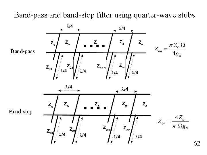
Band-pass and band-stop filter using quarter-wave stubs Band-pass Band-stop 62
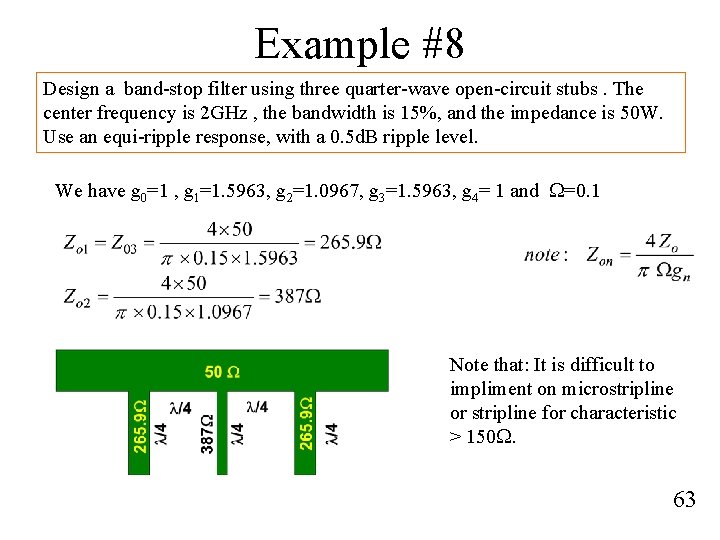
Example #8 Design a band-stop filter using three quarter-wave open-circuit stubs. The center frequency is 2 GHz , the bandwidth is 15%, and the impedance is 50 W. Use an equi-ripple response, with a 0. 5 d. B ripple level. We have g 0=1 , g 1=1. 5963, g 2=1. 0967, g 3=1. 5963, g 4= 1 and W=0. 1 Note that: It is difficult to impliment on microstripline or stripline for characteristic > 150 W. 63
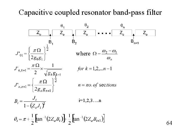
Capacitive coupled resonator band-pass filter where i=1, 2, 3…. n 64
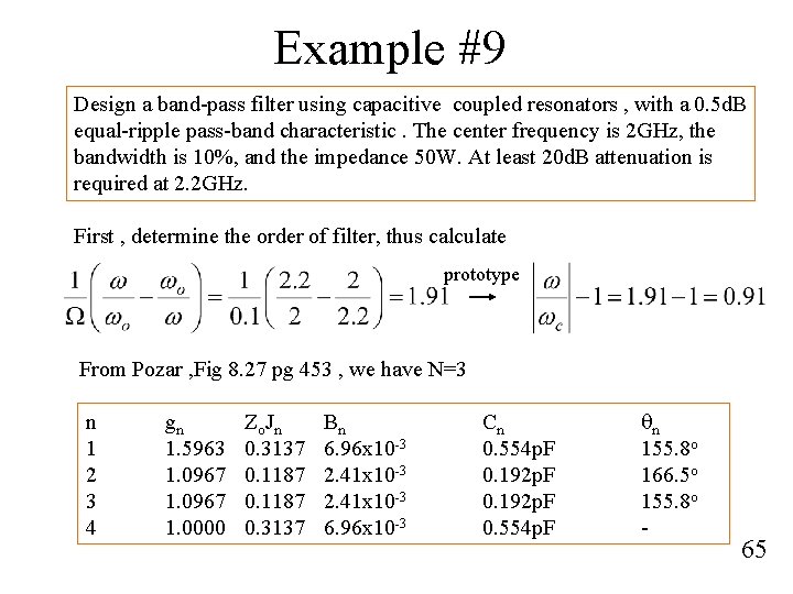
Example #9 Design a band-pass filter using capacitive coupled resonators , with a 0. 5 d. B equal-ripple pass-band characteristic. The center frequency is 2 GHz, the bandwidth is 10%, and the impedance 50 W. At least 20 d. B attenuation is required at 2. 2 GHz. First , determine the order of filter, thus calculate prototype From Pozar , Fig 8. 27 pg 453 , we have N=3 n 1 2 3 4 gn 1. 5963 1. 0967 1. 0000 Z o Jn 0. 3137 0. 1187 0. 3137 Bn 6. 96 x 10 -3 2. 41 x 10 -3 6. 96 x 10 -3 Cn 0. 554 p. F 0. 192 p. F 0. 554 p. F qn 155. 8 o 166. 5 o 155. 8 o - 65
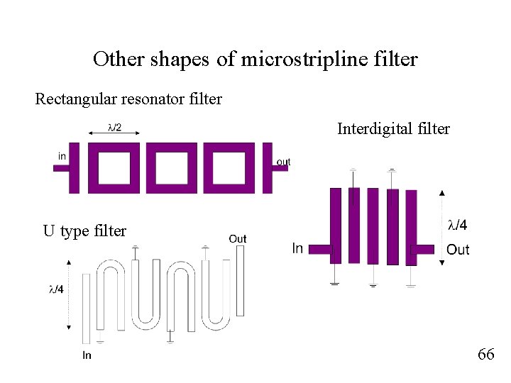
Other shapes of microstripline filter Rectangular resonator filter Interdigital filter U type filter 66
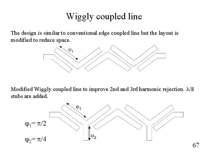
Wiggly coupled line The design is similar to conventional edge coupled line but the layout is modified to reduce space. Modified Wiggly coupled line to improve 2 nd and 3 rd harmonic rejection. l/8 stubs are added. j 1= p/2 j 2= p/4 67
- Slides: 67