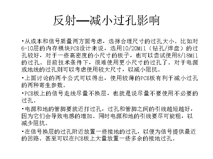
Microstrip 1 foot 12 inch 1 inch 2


 Hot Air Level Soldering �� (HASL) Entek/OSP(防氧化)板 Carbon Oil 碳油板 Peelable Mask")
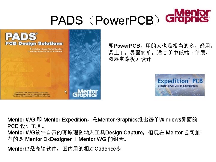
、Mentor WG •")
 Front-end PCB design(PCB前端设计) Front-end PCB design")
 AMS simulation(AMS仿真) Finding problems early with")
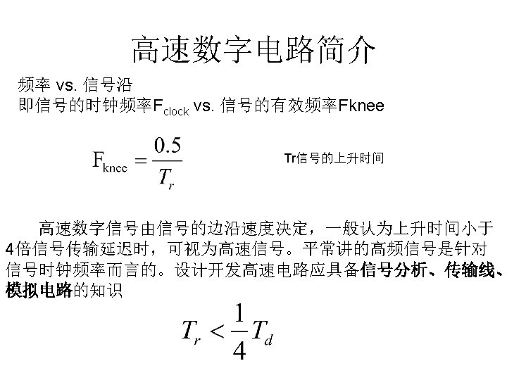
 Signal and power integrity(信号与电源完整性) Stresses on")

 Design entry HDL:原理图绘制(可定制,但通用性低、不易转换其它格式) Design")
- Slides: 52
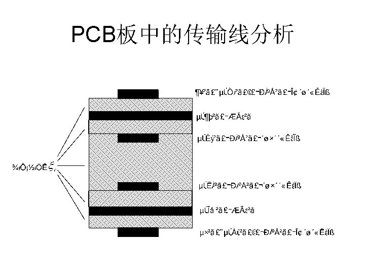
微带线 Microstrip 1 foot = 12 inch 1 inch = 2. 54 cm 1 inch = 1000 mils 1英寸 = 1000密耳 1 oz = 1. 44 mils 1盎司=1. 44密耳 原: 1 oz = 31. 1 g 克 在PCB板上,一平方 英寸的铜箔,厚度为 1. 44 mils时,质量为 1 oz。
微带线 Microstrip
微带线 Microstrip
带状线 Stripline 1 foot = 12 inch 1 inch = 2. 54 cm 1 inch = 1000 mils 1英寸 = 1000密耳 1 oz = 1. 44 mils 1盎司=1. 44密耳
带状线 Stripline
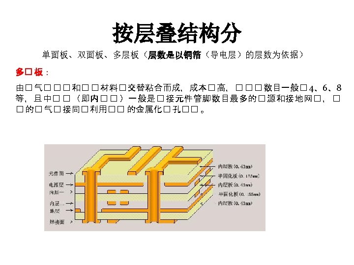
带状线 Stripline PCB简介
按表面制作分:(solder. Surface) Hot Air Level Soldering �� (HASL) Entek/OSP(防氧化)板 Carbon Oil 碳油板 Peelable Mask � 胶板 Gold Finger 金手指板 Immersion Gold 沉金板 Gold Plating � 金 Immersion Tin 沉� 板 Immersion Silver 沉� 板(D 2厂) 按用途分: 通信/耗用性� 子/� 用/� 算机/半� 体/�� 板…, BGA等
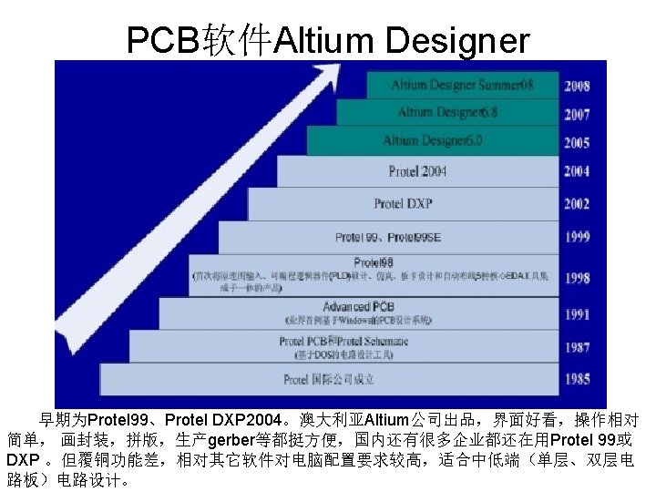
PCB EDA 软件简介 • Cadence Allegro • Altium Designer • PADS(Power. PCB)、Mentor WG • Cadence Allegro组件介绍
Cadence Allegro SPB ( Silicon Package Board ) Front-end PCB design(PCB前端设计) Front-end PCB design requires functional conflict resolution and the unambiguous capture of goals and constraints. Cadence® technology supports multiple design approaches for accurate simulations and tradeoffs. PCB前端设计(电路原理图)需要明确设计目的、解决功能冲突、设计规则参数。 Cadence®提供多种设计仿真分析方法。 FPGA-PCB co-design(FPGA-PCB协同设计) Integrating large-pin-count FPGAs with many different types of user-configurable pins and assignment rules extends the time to do pin assignment. Manual pin assignment approaches can extend design cycles and increase the risk of unnecessary PCB respins. Cadence replaces manual and error-prone processes with two placement-aware technologies that automate pin assignment. FPGA集成了很多不同类型的引脚,电路板设计时,手 分配这些引脚要花很多时间, 且PCB返 的风险极大。Cadence的自动分配引脚技术代替人 绘制,避免人 失误。
Cadence Allegro SPB ( Silicon Package Board ) AMS simulation(AMS仿真) Finding problems early with accurate simulations before fabrication saves time and budget. Cadence® analog/mixed-signal (AMS) simulators enable accurate modeling, verification, and optimization of designs to reduce risk. 在PCB生产前,精确的仿真能节约时间与金钱。 Cadence® 的混合信号仿真软件能够通 过精确建模、验证、优化设计以降低风险。 Layout and routing(布局和布线) Shrinking design cycles and a growing number of nets with constraints require customers to adopt PCB design methodologies that increase predictability and accelerate design turnaround. Cadence® layout and routing technology offers a scalable, easy-to-use, constraint-driven PCB design solution for simple to complex PCBs, including those with RF etch components. 为了减少设计周期、连线的限制越来越多,要求设计者用的PCB设计软件拥有可预测性 并能加快设计周期。 Cadence® 布局和布线 具提供可扩展、易用、从单层到多层电路 板、射频元件制作等印刷电路板约束规则的设计解决方案。
Cadence Allegro SPB ( Silicon Package Board ) Signal and power integrity(信号与电源完整性) Stresses on signal and power integrity grow with every increase in speed, complexity, and miniaturization. Cadence® technology helps you address everything from simple electrical analysis to multi-board signal simulations in the multi-gigabit range. 电路板的速度越快、功能越多、面积越小,对信号与电路的完整必要求越高。 Cadence可从简单电气分析到多层电路板信号完整性分析,进行高达GHz以上的仿真。 Library and design data management(数据管理) Desktop access to current component information and design data is vital to costeffective, on-time project delivery. The Cadence® library and design data management environment provides advanced features for intra-company and design chain collaboration and control. 高效、及时交付项目,需要提供设计软件版本、设计数据。Cadence® 的数据管理功能 便宜公司内部设计团队管理与协同合作。
国内公司使用的EDA 具 Intel: Concept+Allegro+ Specctra. Quest Dell: DXD+ Allegro + SQ原理图也有一部分是 Capture Huawei:viewdraw+ Allegro + Specctra. Quest+Exp. EDAtion ZTE: Concept+Allegro+ Specctra. Quest+Exp. EDAtion UT: Concept+Allegro、Power. PCB+ Specctra. Quest Csico:Concept+Allegro+ Specctra. Quest Hp: Concept+Allegro+ Specctra. Quest 从 Boardstation转成 Alllegro 流程 Moto: Concept+Allegro+ Specctra. Quest 从 Boardstation转成 Alllegro 流程 Nokia: Mentor BA+ ZUKEN BD CHIPCON(TI):CADSTAR
Cadence Allegro 16. 3组件 Cadence Help: 帮助文档 Design entry CIS:原理图绘制(应用广泛、可以转换到Mentor和PADS) Design entry HDL:原理图绘制(可定制,但通用性低、不易转换其它格式) Design entry rules checker(HDL的规则检查 具) FPGA System Planner: Or. CAD 相关:原Or. CAD公司的设计 具融合至Cadence Package designer:IC封装设计和分析 PCB editor:完整的PCB设计软件 PCB router:CCT布线器 PCB SI:建立数字PCB系统和集成电路封装设计的集成高速设计和分析环境 Physical viewer: Project Manager:Design Entry HDL 的项目管理器 PSpice AD:原Or. CAD公司的仿真 具 PSpice AA:原Or. CAD公司的仿真 具 Sig. Xplorer:网络拓扑的提取和仿真 Si. P: Si. P Digital Architect: System Architect: AMS Simulator:混合信号仿真系统 PCB Editor Utilities:包含PAD Design、DB Doctor、Batch DRC等 PSpice Accessories:仿真 具附件