Microscopic radiation damage in semiconductor detectors M Bruzzi
Microscopic radiation damage in semiconductor detectors M. Bruzzi Univ. Firenze INFN Sezione Firenze Università di Firenze, Italy Microscopic radiation damage in semiconductor detectors M. Bruzzi, Legnaro, 15 Aprile 2013

Motivation Semiconductor detectors have a number of potential applications where radiation induced defects plays a crucial role. Environment Radiation type Typical exposure Fission reactor 0. 1 -5 Me. V n 5 x 10¹⁷ m-2 s-1 Fusion reactor 0. 1 -14 Me. V n 8 x 10¹⁸ m-2 s-1 Space 6 e. V photons 1020 m-2 s-1 10 ke. V-3 Me. Vb 5 x 10¹² m-2 s-1 1 Me. V-300 Me. V p 4 x 10⁹ m-2 s-1 15 Me. V p 6 x 10¹⁶ m-2 s-1 Ion accelerator High energy physics n, p , pions experiments 1014 -1016 cm-2 radiotherapy 10 k. Gy X, e, p Microscopic radiation damage in semiconductor detectors M. Bruzzi, Legnaro, 15 Aprile 2013
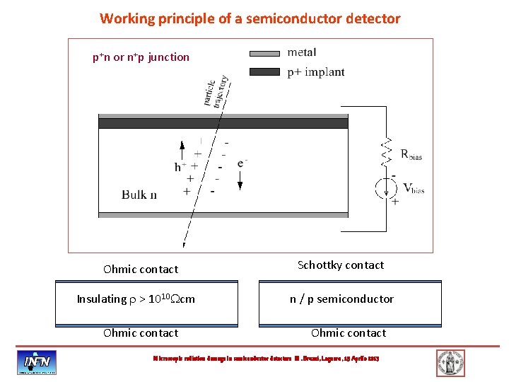
Working principle of a semiconductor detector p+n or n+p junction Ohmic contact Insulating r > 1010 Wcm Ohmic contact Schottky contact n / p semiconductor Ohmic contact Microscopic radiation damage in semiconductor detectors M. Bruzzi, Legnaro, 15 Aprile 2013
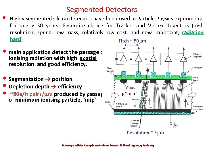
• Segmented Detectors Highly segmented silicon detectors have been used in Particle Physics experiments for nearly 30 years. Favourite choice for Tracker and Vertex detectors (high resolution, speed, low mass, relatively low cost, and now important, radiation hard) Pitch ~ 50 m • main application detect the passage of ionising radiation with high spatial resolution and good efficiency. • Segmentation → position • Depletion depth → efficiency • ~80 e/h pairs/μm produced by passage of minimum ionising particle, ‘mip’ p+ in n- Resolution ~ 5 m Microscopic radiation damage in semiconductor detectors M. Bruzzi, Legnaro, 15 Aprile 2013
![Reminder: Reverse biased abrupt p+-n junction Poisson’s equation Positive space charge, Neff =[P] (ionized Reminder: Reverse biased abrupt p+-n junction Poisson’s equation Positive space charge, Neff =[P] (ionized](http://slidetodoc.com/presentation_image/65897ced496156e2db629ceb79a2e5a2/image-5.jpg)
Reminder: Reverse biased abrupt p+-n junction Poisson’s equation Positive space charge, Neff =[P] (ionized Phosphorus atoms) Electrical charge density Electrical field strength Full charge collection only for VB>Vdep ! depletion voltage Electron potential energy effective space charge density Microscopic radiation damage in semiconductor detectors M. Bruzzi, Legnaro, 15 Aprile 2013
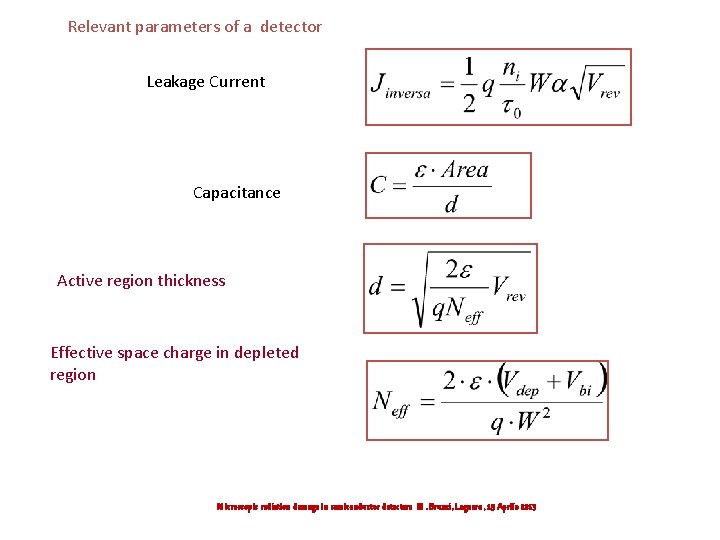
Relevant parameters of a detector Leakage Current Capacitance Active region thickness Effective space charge in depleted region Microscopic radiation damage in semiconductor detectors M. Bruzzi, Legnaro, 15 Aprile 2013

Semiconductor s proposed for detector applications Microscopic radiation damage in semiconductor detectors M. Bruzzi, Legnaro, 15 Aprile 2013
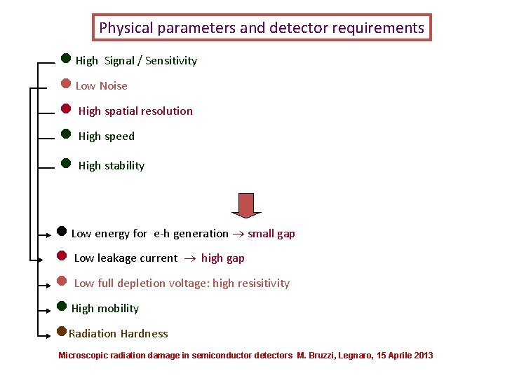
Physical parameters and detector requirements High Signal / Sensitivity Low Noise High spatial resolution High speed High stability Low energy for e-h generation small gap Low leakage current high gap Low full depletion voltage: high resisitivity High mobility Radiation Hardness Microscopic radiation damage in semiconductor detectors M. Bruzzi, Legnaro, 15 Aprile 2013

Radiation Damage Mechanisms in Semiconductor Devices Microscopic Damage Traps Recombination centres Radiation induced defects Extended defects or clusters Carrier removal and increase of resistivity Midgap Fermi level pinning Macroscopic Damage Increase of the leakage current Change in Neff and space charge sign - underdepletion Decrease of minority carrier lifetime and diffusion length Decrease of the charge collection, sensitivity and energy conversion efficiency Microscopic radiation damage in semiconductor detectors M. Bruzzi, Legnaro, 15 Aprile 2013
Microscopic Radiation Damage Microscopic radiation damage in semiconductor detectors M. Bruzzi, Legnaro, 15 Aprile 2013
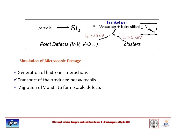
particle Si s Frenkel pair Vacancy + Interstitial EK > 25 e. V Point Defects (V-V, V-O. . ) EK > 5 ke. V clusters Simulation of Microscopic Damage üGeneration of hadronic interactions üTransport of the produced heavy recoils üMigration of V and I to form stable defects Microscopic radiation damage in semiconductor detectors M. Bruzzi, Legnaro, 15 Aprile 2013 V I

Vacancy amount and distribution depends on particle kind and energy 60 Co-gammas Electrons Neutrons (elastic scattering) –Ee > 255 ke. V for displacement – E > 185 e. V for displacement –Compton Electrons n with max. E 1 Me. V –Ee > 8 Me. V for cluster – En > 35 ke. V for cluster (no cluster production) Only point defects & clusters Mainly clusters Initial distribution of vacancies in (1 m)3 after 1014 particles/cm 2 10 Me. V protons 24 Ge. V/c protons 1 Me. V neutrons [Mika Huhtinen NIMA 491(2002) 194] Microscopic radiation damage in semiconductor detectors M. Bruzzi, Legnaro, 15 Aprile 2013
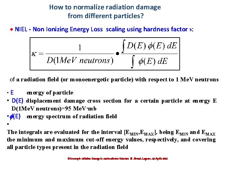
How to normalize radiation damage from different particles? NIEL - Non Ionizing Energy Loss scaling using hardness factor k of a radiation field (or monoenergetic particle) with respect to 1 Me. V neutrons • E energy of particle • D(E) displacement damage cross section for a certain particle at energy E D(1 Me. V neutrons)=95 Me. V·mb • f(E) energy spectrum of radiation field • The integrals are evaluated for the interval [EMIN, EMAX], being EMIN and EMAX the minimum and maximum cut-off energy values, respectively, and covering all particle types present in the radiation field Microscopic radiation damage in semiconductor detectors M. Bruzzi, Legnaro, 15 Aprile 2013
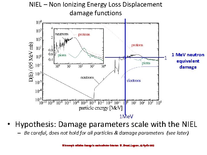
NIEL – Non Ionizing Energy Loss Displacement damage functions 1 Me. V neutron 1 equivalent damage 1 Me. V • Hypothesis: Damage parameters scale with the NIEL – Be careful, does not hold for all particles & damage parameters (see later) Microscopic radiation damage in semiconductor detectors M. Bruzzi, Legnaro, 15 Aprile 2013
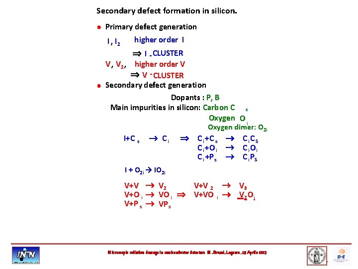
Secondary defect formation in silicon. · Primary defect generation higher order I I , I 2 Þ I -CLUSTER V , V 2 , higher order V Þ V -CLUSTER · Secondary defect generation Dopants : P, B Main impurities in silicon: Carbon C s Oxygen O i I+C s ® Ci Þ Oxygen dimer: O 2 i C i +C s ® C i +O i ® C i +P s ® Ci. CS C i Oi C i PS I + O 2 i → IO 2 i V+V ® V 2 V+O i ® VO i Þ V+P s ® VP s V+V 2 ® V+VO i ® V 3 V 2 Oi Microscopic radiation damage in semiconductor detectors M. Bruzzi, Legnaro, 15 Aprile 2013 -
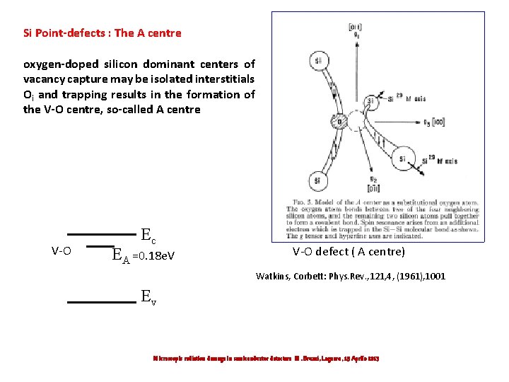
Si Point-defects : The A centre oxygen-doped silicon dominant centers of vacancy capture may be isolated interstitials Oi and trapping results in the formation of the V-O centre, so-called A centre V-O Ec EA =0. 18 e. V V-O defect ( A centre) Watkins, Corbett: Phys. Rev. , 121, 4, (1961), 1001 Ev Microscopic radiation damage in semiconductor detectors M. Bruzzi, Legnaro, 15 Aprile 2013
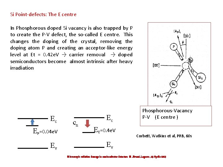
Si Point-defects: The E centre In Phosphorous doped Si vacancy is also trapped by P to create the P-V defect, the so-called E centre. This changes the doping of the crystal, removing the doping atom P and creating an acceptor-like energy level at Et = 0. 42 e. V → carrier removal → doped semiconductors become almost intrinsic after heavy irradiation Ec EP=0. 04 e. V Ev cn Ec EE=0. 4 e. V Phosphorous-Vacancy P-V (E centre ) Corbett, Watkins et al, PRB, 60 s Ev Microscopic radiation damage in semiconductor detectors M. Bruzzi, Legnaro, 15 Aprile 2013
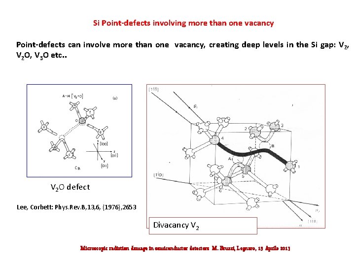
Si Point-defects involving more than one vacancy Point-defects can involve more than one vacancy, creating deep levels in the Si gap: V 2, V 2 O, V 3 O etc. . V 2 O defect Lee, Corbett: Phys. Rev. B, 13, 6, (1976), 2653 Divacancy V 2 Microscopic radiation damage in semiconductor detectors M. Bruzzi, Legnaro, 15 Aprile 2013
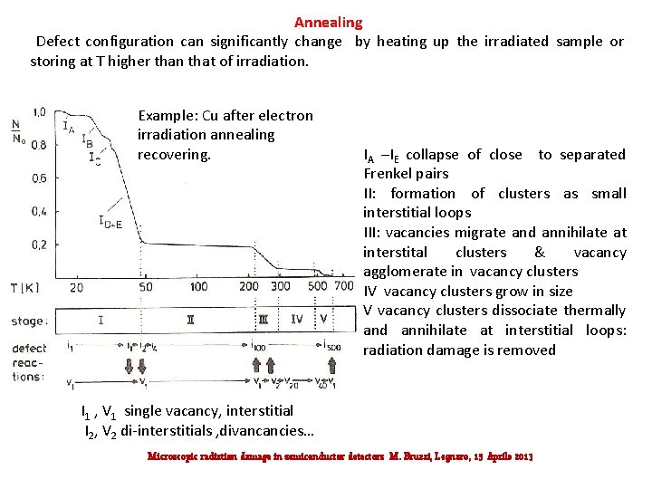
Annealing Defect configuration can significantly change by heating up the irradiated sample or storing at T higher than that of irradiation. Example: Cu after electron irradiation annealing recovering. IA –IE collapse of close to separated Frenkel pairs II: formation of clusters as small interstitial loops III: vacancies migrate and annihilate at interstital clusters & vacancy agglomerate in vacancy clusters IV vacancy clusters grow in size V vacancy clusters dissociate thermally and annihilate at interstitial loops: radiation damage is removed I 1 , V 1 single vacancy, interstitial I 2, V 2 di-interstitials , divancancies… Microscopic radiation damage in semiconductor detectors M. Bruzzi, Legnaro, 15 Aprile 2013
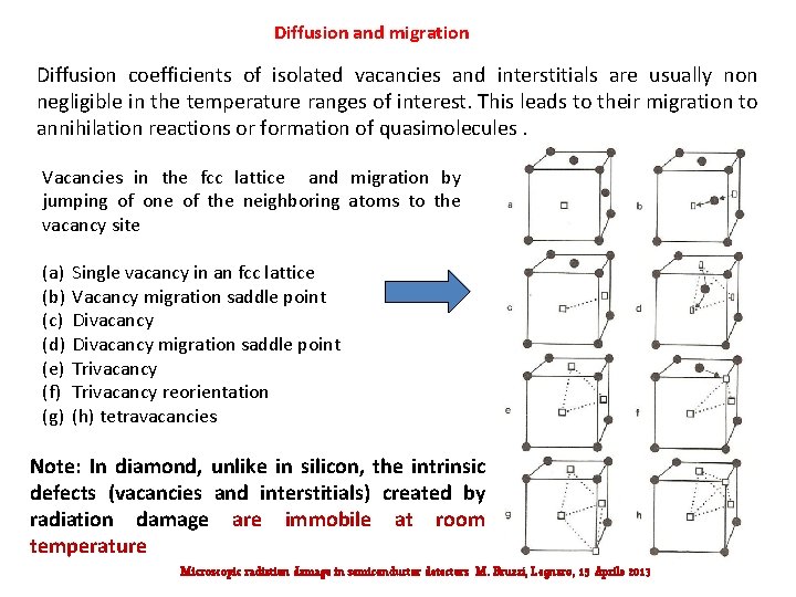
Diffusion and migration Diffusion coefficients of isolated vacancies and interstitials are usually non negligible in the temperature ranges of interest. This leads to their migration to annihilation reactions or formation of quasimolecules. Vacancies in the fcc lattice and migration by jumping of one of the neighboring atoms to the vacancy site (a) (b) (c) (d) (e) (f) (g) Single vacancy in an fcc lattice Vacancy migration saddle point Divacancy migration saddle point Trivacancy reorientation (h) tetravacancies Note: In diamond, unlike in silicon, the intrinsic defects (vacancies and interstitials) created by radiation damage are immobile at room temperature Microscopic radiation damage in semiconductor detectors M. Bruzzi, Legnaro, 15 Aprile 2013
Native Impurity Defects in Diamond Natural diamonds most commonly have N present in aggregated forms, and some rare samples contain boron and are semiconducting. High-temperature–high-pressure synthetic diamonds may contain isolated substitutional nitrogen if getters have not been employed, and, where Ni is present in as part of the solvent-catalyst, a range of Ni-related defects. CVD diamond commonly contains isolated impurity defects including nitrogen, silicon and boron. Hydrogen plays a role in the formation of electrically active defects. Charge Character of defects in diamond : general trends As a general trend substitutional chalcogen impurities yield relatively deep donor levels and dangling bonds yield deep acceptor states, where all dangling bonds are saturated (VH , VNH , etc. ) the defect becomes passive. For this reason diamond has a naturally slightly p-type character.
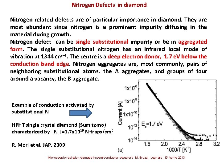
Nitrogen Defects in diamond Nitrogen related defects are of particular importance in diamond. They are most abundant since nitrogen is a prominent impurity diffusing in the material during growth. Nitrogen defect can be single substitutional impurity or be in aggregated form. The single substitutional nitrogen has an infrared local mode of vibration at 1344 cm– 1. The centre is a deep electron donor, 1. 7 e. V below the conduction band edge. Nitrogen aggregates are, most commonly, pairs of neighboring substitutional atoms, the A aggregates, and groups of four around a vacancy, the B aggregate. Example of conduction activated by substitutional N HPHT single crystal diamond (Sumitomo) characterized by [N ] =1. 7 x 10¹⁹ N-traps/cm 3 R. Mori et al. JAP, 2009 Microscopic radiation damage in semiconductor detectors M. Bruzzi, Legnaro, 15 Aprile 2013
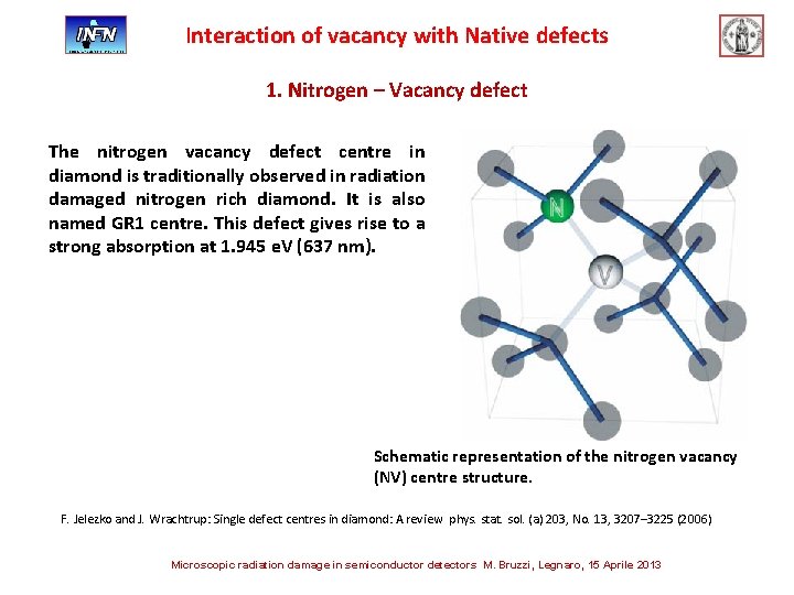
Interaction of vacancy with Native defects 1. Nitrogen – Vacancy defect The nitrogen vacancy defect centre in diamond is traditionally observed in radiation damaged nitrogen rich diamond. It is also named GR 1 centre. This defect gives rise to a strong absorption at 1. 945 e. V (637 nm). Schematic representation of the nitrogen vacancy (NV) centre structure. F. Jelezko and J. Wrachtrup: Single defect centres in diamond: A review phys. stat. sol. (a) 203, No. 13, 3207– 3225 (2006) Microscopic radiation damage in semiconductor detectors M. Bruzzi, Legnaro, 15 Aprile 2013
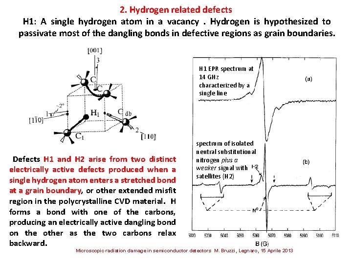
2. Hydrogen related defects H 1: A single hydrogen atom in a vacancy. Hydrogen is hypothesized to passivate most of the dangling bonds in defective regions as grain boundaries. H 1 EPR spectrum at 14 GHz characterized by a single line Defects H 1 and H 2 arise from two distinct electrically active defects produced when a single hydrogen atom enters a stretched bond at a grain boundary, or other extended misfit region in the polycrystalline CVD material. H forms a bond with one of the carbons, producing an electrically active dangling bond on the other as the two carbons relax backward. spectrum of isolated neutral substitutional nitrogen plus a weaker signal with satellites (H 2) Microscopic radiation damage in semiconductor detectors M. Bruzzi, Legnaro, 15 Aprile 2013
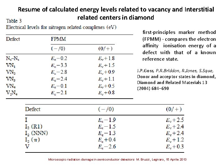
Resume of calculated energy levels related to vacancy and Interstitial related centers in diamond first-principles marker method (FPMM) - compares the electron affinity ionisation energy of a defect with that of a known reference state. J. P. Goss, P. R. Briddon, R. Jones, S. Sque, Donor and acceptor states in diamond, Diamond and Related Materials 13 (2004) 684– 690 Microscopic radiation damage in semiconductor detectors M. Bruzzi, Legnaro, 15 Aprile 2013
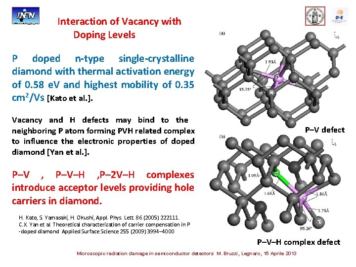
3. Interaction of Vacancy with Doping Levels P doped n-type single-crystalline diamond with thermal activation energy of 0. 58 e. V and highest mobility of 0. 35 cm 2/Vs [Kato et al. ]. Vacancy and H defects may bind to the neighboring P atom forming PVH related complex to influence the electronic properties of doped diamond [Yan et al. ]. P–V defect P–V , P–V–H , P– 2 V–H complexes introduce acceptor levels providing hole carriers in diamond. H. Kato, S. Yamasaki, H. Okushi, Appl. Phys. Lett. 86 (2005) 222111. C. X. Yan et al. Theoretical characterization of carrier compensation in P -doped diamond Applied Surface Science 255 (2009) 3994– 4000 P–V–H complex defect Microscopic radiation damage in semiconductor detectors M. Bruzzi, Legnaro, 15 Aprile 2013
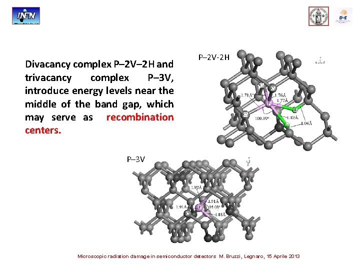
Divacancy complex P– 2 V– 2 H and trivacancy complex P– 3 V, introduce energy levels near the middle of the band gap, which may serve as recombination centers. P– 2 V-2 H P– 3 V Microscopic radiation damage in semiconductor detectors M. Bruzzi, Legnaro, 15 Aprile 2013
Electrical activity of energy levels related to defects Microscopic radiation damage in semiconductor detectors M. Bruzzi, Legnaro, 15 Aprile 2013
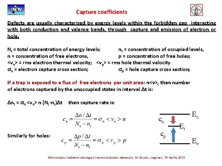
Capture coefficients Defects are usually characterised by energy levels within the forbidden gap interacting with both conduction and valence bands, through capture and emission of electron or hole. Nt = total concentration of energy levels; nt = concentration of occupied levels, n = concentration of free electrons, p = concentration of free holes; <vn> = rms electron thermal velocity; <vp> = rms hole thermal velocity sn = electron capture cross section; sp = hole capture cross section; If a trap is exposed to a flux of free electrons per unit area: n<v>, then number of electrons captured by the unoccupied states in interval t is: nt = sn <vn> n (Nt-nt) t then capture rate is: cn Similarly for holes: cp Ec Et Microscopic radiation damage in semiconductor detectors M. Bruzzi, Legnaro, 15 Aprile 2013 Ev
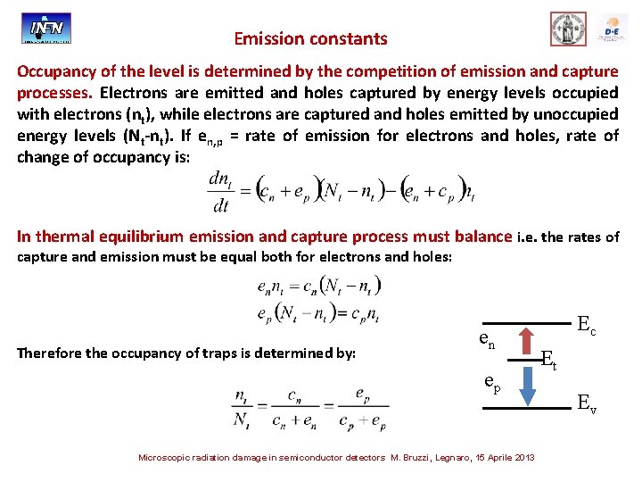
Emission constants Occupancy of the level is determined by the competition of emission and capture processes. Electrons are emitted and holes captured by energy levels occupied with electrons (nt), while electrons are captured and holes emitted by unoccupied energy levels (Nt-nt). If en, p = rate of emission for electrons and holes, rate of change of occupancy is: In thermal equilibrium emission and capture process must balance i. e. the rates of capture and emission must be equal both for electrons and holes: Therefore the occupancy of traps is determined by: en ep Microscopic radiation damage in semiconductor detectors M. Bruzzi, Legnaro, 15 Aprile 2013 Ec Et Ev
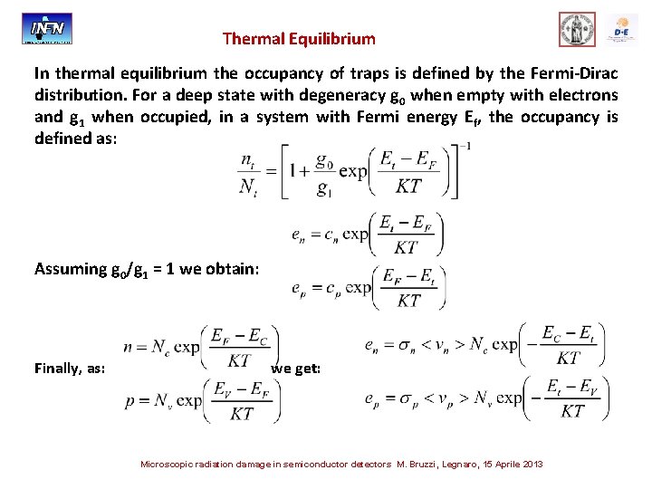
Thermal Equilibrium In thermal equilibrium the occupancy of traps is defined by the Fermi-Dirac distribution. For a deep state with degeneracy g 0 when empty with electrons and g 1 when occupied, in a system with Fermi energy Ef, the occupancy is defined as: Assuming g 0/g 1 = 1 we obtain: Finally, as: we get: Microscopic radiation damage in semiconductor detectors M. Bruzzi, Legnaro, 15 Aprile 2013
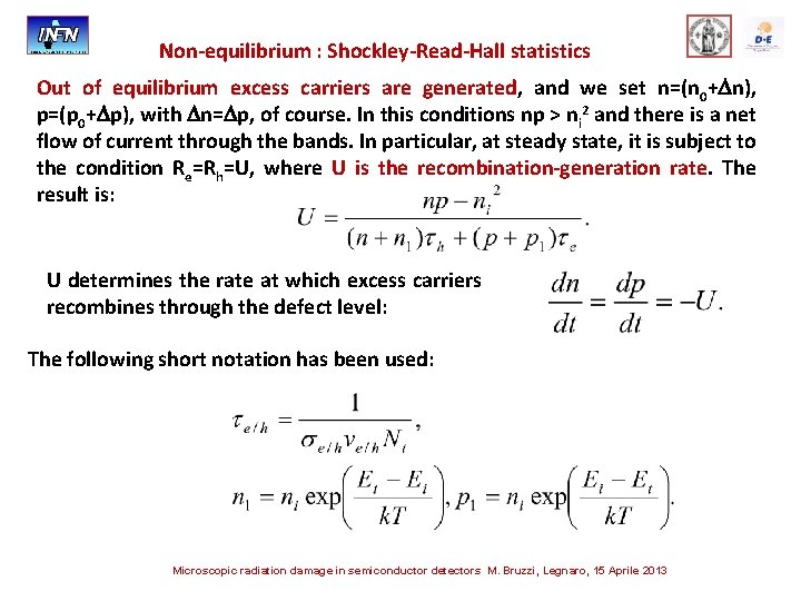
Non-equilibrium : Shockley-Read-Hall statistics Out of equilibrium excess carriers are generated, and we set n=(n 0+ n), p=(p 0+ p), with n= p, of course. In this conditions np > ni 2 and there is a net flow of current through the bands. In particular, at steady state, it is subject to the condition Re=Rh=U, where U is the recombination-generation rate. The result is: U determines the rate at which excess carriers recombines through the defect level: The following short notation has been used: Microscopic radiation damage in semiconductor detectors M. Bruzzi, Legnaro, 15 Aprile 2013
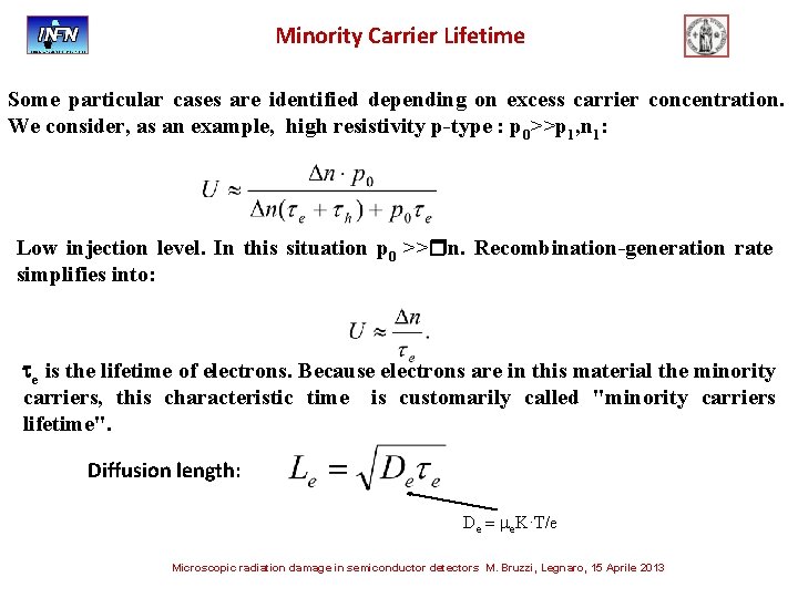
Minority Carrier Lifetime Some particular cases are identified depending on excess carrier concentration. We consider, as an example, high resistivity p-type : p 0>>p 1, n 1: Low injection level. In this situation p 0 >> n. Recombination-generation rate simplifies into: e is the lifetime of electrons. Because electrons are in this material the minority carriers, this characteristic time is customarily called "minority carriers lifetime". Diffusion length: De = e. K·T/e Microscopic radiation damage in semiconductor detectors M. Bruzzi, Legnaro, 15 Aprile 2013
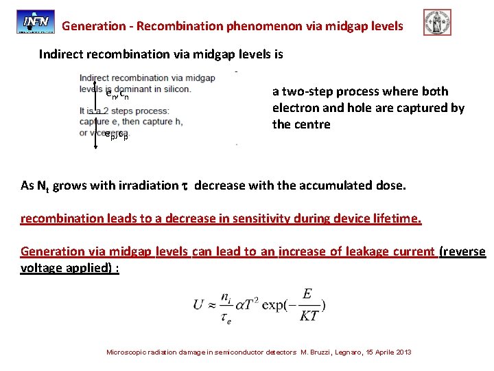
Generation - Recombination phenomenon via midgap levels Indirect recombination via midgap levels is en, cn ep, cp a two-step process where both electron and hole are captured by the centre As Nt grows with irradiation decrease with the accumulated dose. recombination leads to a decrease in sensitivity during device lifetime. Generation via midgap levels can lead to an increase of leakage current (reverse voltage applied) : Microscopic radiation damage in semiconductor detectors M. Bruzzi, Legnaro, 15 Aprile 2013
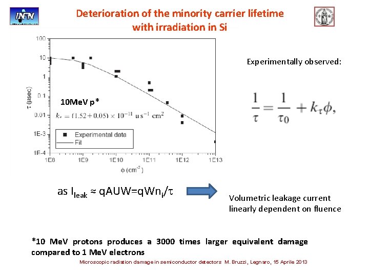
Deterioration of the minority carrier lifetime with irradiation in Si Experimentally observed: 10 Me. V p* as Ileak ≈ q. AUW=q. Wni/ Volumetric leakage current linearly dependent on fluence *10 Me. V protons produces a 3000 times larger equivalent damage compared to 1 Me. V electrons Microscopic radiation damage in semiconductor detectors M. Bruzzi, Legnaro, 15 Aprile 2013
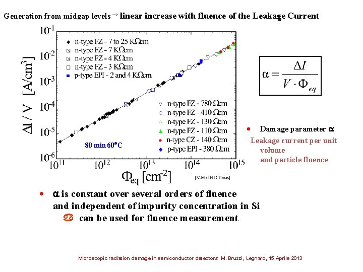
Generation from midgap levels → linear increase with fluence of the Leakage Current 80 min 60 C Damage parameter Leakage current per unit volume and particle fluence is constant over several orders of fluence and independent of impurity concentration in Si can be used for fluence measurement Microscopic radiation damage in semiconductor detectors M. Bruzzi, Legnaro, 15 Aprile 2013
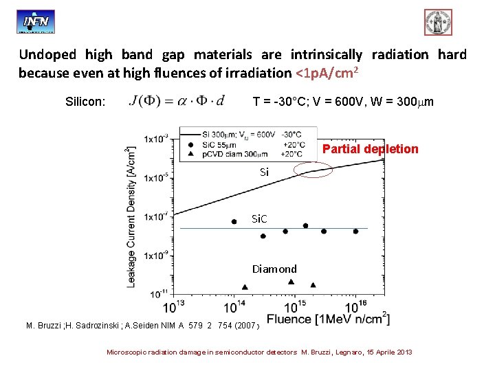
Undoped high band gap materials are intrinsically radiation hard because even at high fluences of irradiation <1 p. A/cm 2 Silicon: T = -30°C; V = 600 V, W = 300 m Partial depletion Si Si. C Diamond M. Bruzzi ; H. Sadrozinski ; A. Seiden NIM A 579 2 754 (2007 ) Microscopic radiation damage in semiconductor detectors M. Bruzzi, Legnaro, 15 Aprile 2013
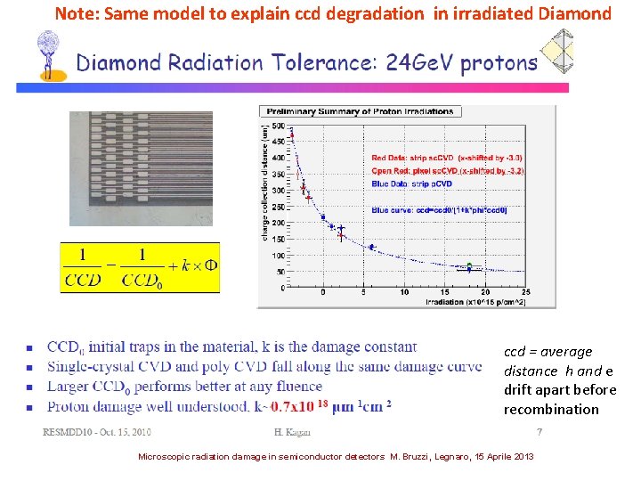
Note: Same model to explain ccd degradation in irradiated Diamond ccd = average distance h and e drift apart before recombination Microscopic radiation damage in semiconductor detectors M. Bruzzi, Legnaro, 15 Aprile 2013
Microscopic Radiation Damage Analysis: non spectroscopic methods Microscopic radiation damage in semiconductor detectors M. Bruzzi, Legnaro, 15 Aprile 2013
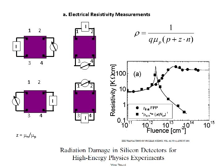
a. Electrical Resistivity Measurements 2 1 I 1 2 I 3 1 4 2 3 4 1 2 3 4 I z = n/ p 4 I 3
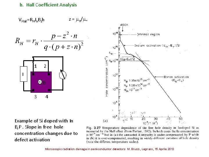
b. Hall Coefficient Analysis z = n/ p VHall=RHJx. Bzh 1 2 I B 3 4 Example of Si doped with In B, P. Slope in free hole concentration changes due to defect activation Microscopic radiation damage in semiconductor detectors M. Bruzzi, Legnaro, 15 Aprile 2013
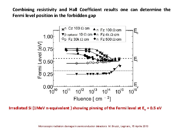
Combining resistivity and Hall Coefficient results one can determine the Fermi level position in the forbidden gap Irradiated Si (1 Me. V n-equivalent ) showing pinning of the Fermi level at Ev + 0. 5 e. V Microscopic radiation damage in semiconductor detectors M. Bruzzi, Legnaro, 15 Aprile 2013

How to detect electrically active defects ? Defect Spectroscopy in semiconductors 1. Thermally Stimulated Currents TSC 2. Deep Level Transient Spectroscopy DLTS 3. Photo Induced Current Transient Spectroscopy PICTS Microscopic radiation damage in semiconductor detectors M. Bruzzi, Legnaro, 15 Aprile 2013
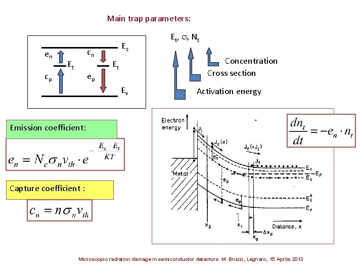
Main trap parameters: en cp cn Et ep Ec Et, , Nt Concentration Cross section Et Ev Activation energy Emission coefficient: Capture coefficient : Microscopic radiation damage in semiconductor detectors M. Bruzzi, Legnaro, 15 Aprile 2013
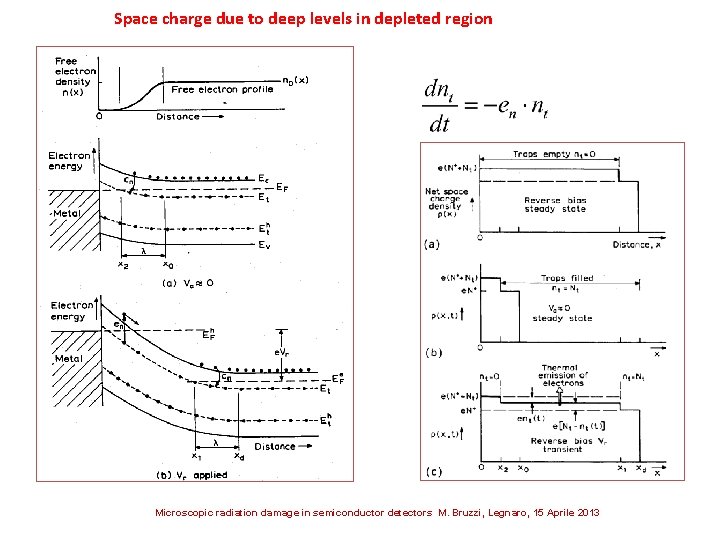
Space charge due to deep levels in depleted region Microscopic radiation damage in semiconductor detectors M. Bruzzi, Legnaro, 15 Aprile 2013
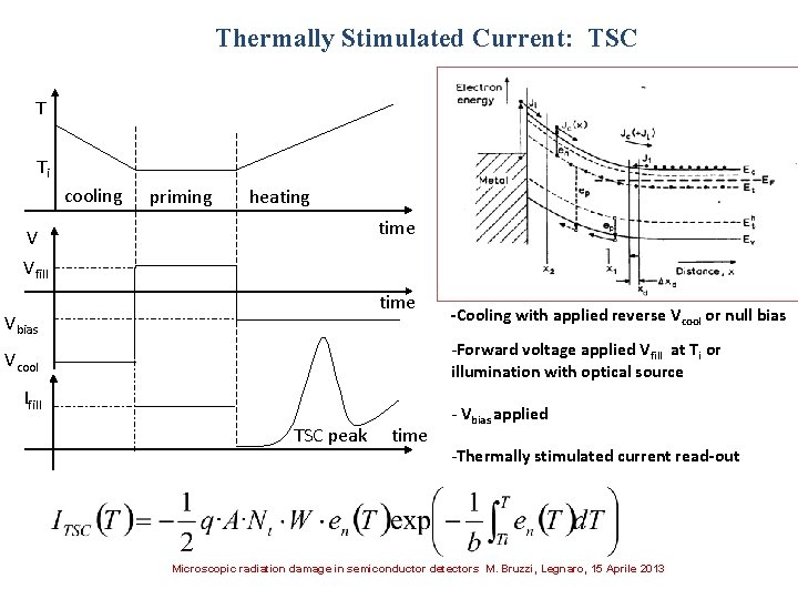
Thermally Stimulated Current: TSC T Ti cooling priming heating time V Vfill time Vbias -Cooling with applied reverse Vcool or null bias -Forward voltage applied Vfill at Ti or illumination with optical source Vcool Ifill TSC peak time - Vbias applied -Thermally stimulated current read-out Microscopic radiation damage in semiconductor detectors M. Bruzzi, Legnaro, 15 Aprile 2013
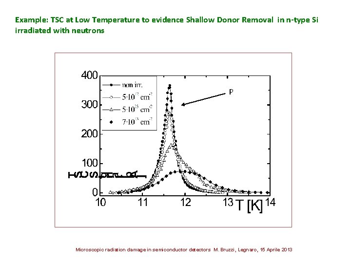
Example: TSC at Low Temperature to evidence Shallow Donor Removal in n-type Si irradiated with neutrons P Microscopic radiation damage in semiconductor detectors M. Bruzzi, Legnaro, 15 Aprile 2013
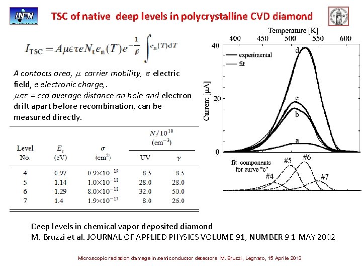
TSC of native deep levels in polycrystalline CVD diamond A contacts area, m carrier mobility, e electric field, e electronic charge, . met = ccd average distance an hole and electron drift apart before recombination, can be measured directly. Deep levels in chemical vapor deposited diamond M. Bruzzi et al. JOURNAL OF APPLIED PHYSICS VOLUME 91, NUMBER 9 1 MAY 2002 Microscopic radiation damage in semiconductor detectors M. Bruzzi, Legnaro, 15 Aprile 2013
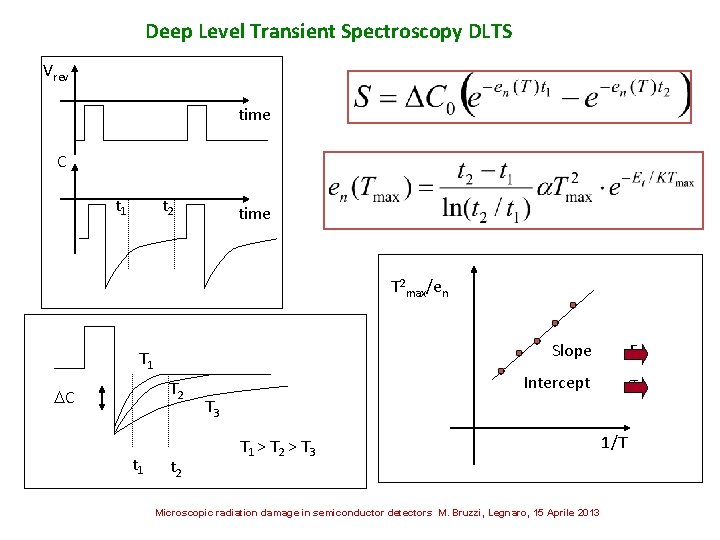
Deep Level Transient Spectroscopy DLTS Vrev time C t 1 t 2 time T 2 max/en Slope Et T 1 T 2 C t 1 t 2 Intercept T 3 T 1 > T 2 > T 3 Microscopic radiation damage in semiconductor detectors M. Bruzzi, Legnaro, 15 Aprile 2013 1/T
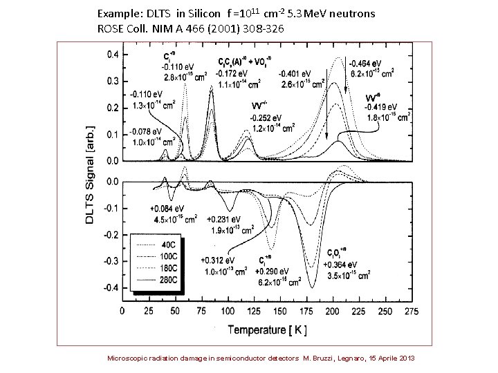
Example: DLTS in Silicon f =1011 cm-2 5. 3 Me. V neutrons ROSE Coll. NIM A 466 (2001) 308 -326 Microscopic radiation damage in semiconductor detectors M. Bruzzi, Legnaro, 15 Aprile 2013
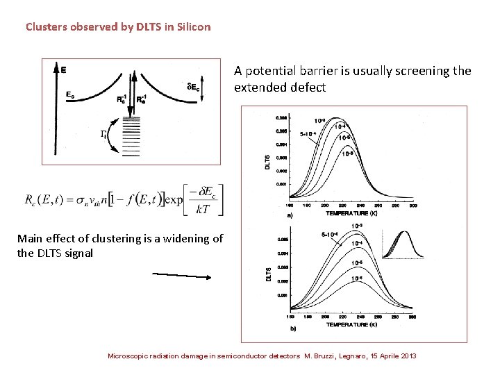
Clusters observed by DLTS in Silicon A potential barrier is usually screening the extended defect Main effect of clustering is a widening of the DLTS signal Microscopic radiation damage in semiconductor detectors M. Bruzzi, Legnaro, 15 Aprile 2013
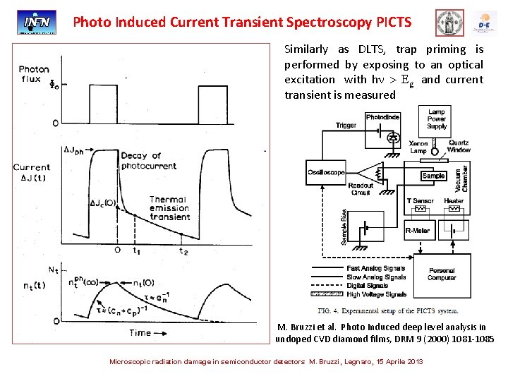
Photo Induced Current Transient Spectroscopy PICTS Similarly as DLTS, trap priming is performed by exposing to an optical excitation with hn > Eg and current transient is measured M. Bruzzi et al. Photo Induced deep level analysis in undoped CVD diamond films, DRM 9 (2000) 1081 -1085 Microscopic radiation damage in semiconductor detectors M. Bruzzi, Legnaro, 15 Aprile 2013
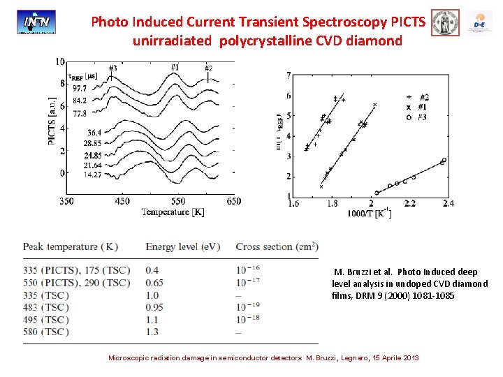
Photo Induced Current Transient Spectroscopy PICTS in unirradiated polycrystalline CVD diamond M. Bruzzi et al. Photo Induced deep level analysis in undoped CVD diamond films, DRM 9 (2000) 1081 -1085 Microscopic radiation damage in semiconductor detectors M. Bruzzi, Legnaro, 15 Aprile 2013
Impact of Defects on Detector properties Microscopic radiation damage in semiconductor detectors M. Bruzzi, Legnaro, 15 Aprile 2013
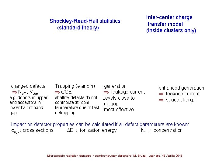
Shockley-Read-Hall statistics (standard theory) Inter-center charge transfer model (inside clusters only) charged defects Neff , Vdep Trapping (e and h) CCE e. g. donors in upper and acceptors in lower half of band gap generation leakage current shallow defects do not Levels close to contribute at room midgap temperature due to fast most effective enhanced generation leakage current space charge detrapping Impact on detector properties can be calculated if all defect parameters are known: n, p : cross sections E : ionization energy Nt : concentration Microscopic radiation damage in semiconductor detectors M. Bruzzi, Legnaro, 15 Aprile 2013
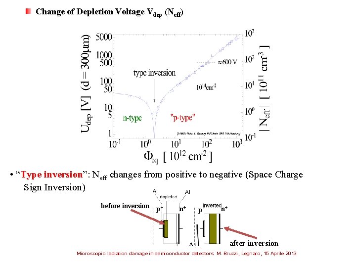
Change of Depletion Voltage Vdep (Neff) • “Type inversion”: Neff changes from positive to negative (Space Charge Sign Inversion) before inversion p+ n+ after inversion Microscopic radiation damage in semiconductor detectors M. Bruzzi, Legnaro, 15 Aprile 2013
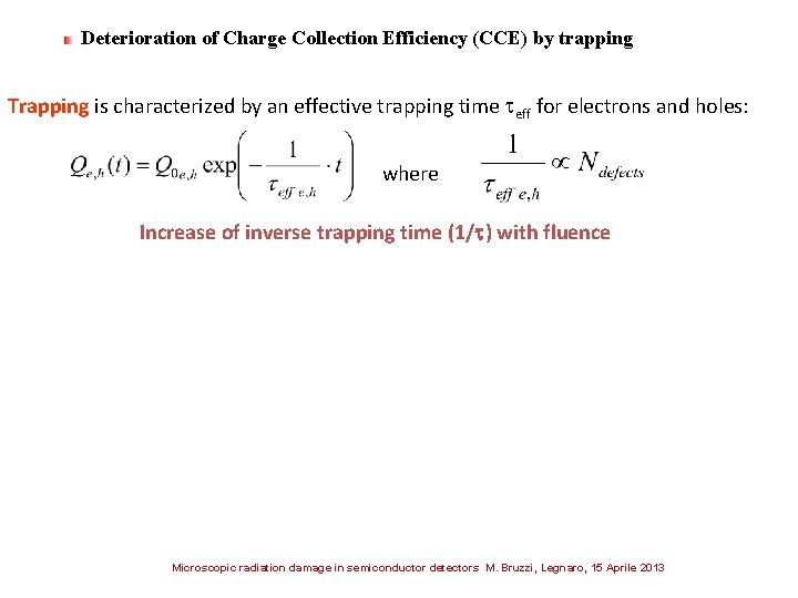
Deterioration of Charge Collection Efficiency (CCE) by trapping Trapping is characterized by an effective trapping time eff for electrons and holes: where Increase of inverse trapping time (1/ ) with fluence Microscopic radiation damage in semiconductor detectors M. Bruzzi, Legnaro, 15 Aprile 2013
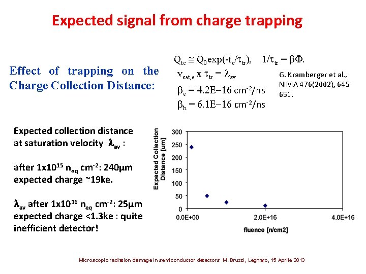
Expected signal from charge trapping Effect of trapping on the Charge Collection Distance: Qtc Q 0 exp(-tc/ tr), vsat, e x tr = lav 1/ tr = b. F. be = 4. 2 E-16 cm-2/ns bh = 6. 1 E-16 cm-2/ns G. Kramberger et al. , NIMA 476(2002), 645651. Expected collection distance at saturation velocity lav : after 1 x 10¹⁵ neq cm-2: 240µm expected charge ~19 ke. lav after 1 x 10¹⁶ neq cm-2: 25µm expected charge <1. 3 ke : quite inefficient detector! Microscopic radiation damage in semiconductor detectors M. Bruzzi, Legnaro, 15 Aprile 2013
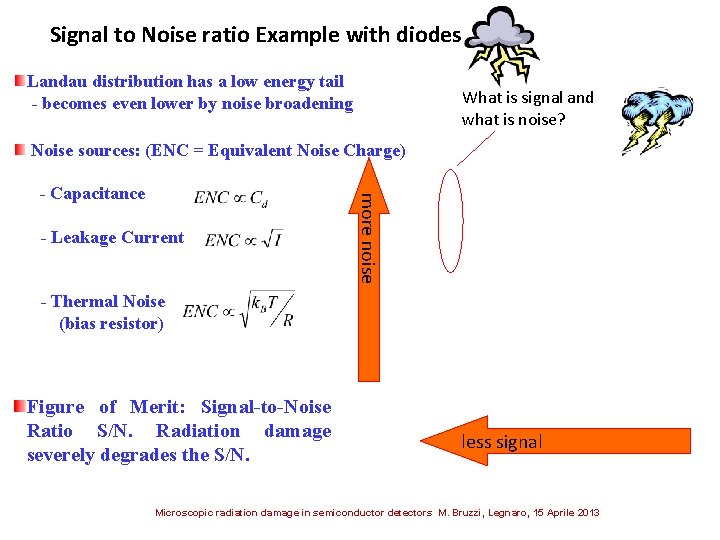
Signal to Noise ratio Example with diodes Landau distribution has a low energy tail - becomes even lower by noise broadening What is signal and what is noise? more noise Noise sources: (ENC = Equivalent Noise Charge) - Capacitance - Leakage Current - Thermal Noise (bias resistor) Figure of Merit: Signal-to-Noise Ratio S/N. Radiation damage severely degrades the S/N. less signal Microscopic radiation damage in semiconductor detectors M. Bruzzi, Legnaro, 15 Aprile 2013
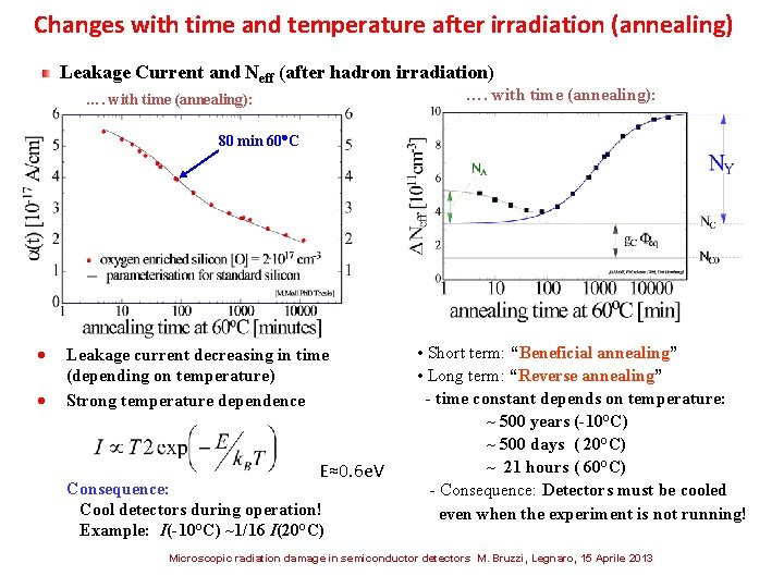
Changes with time and temperature after irradiation (annealing) Leakage Current and Neff (after hadron irradiation) …. with time (annealing): 80 min 60 C Leakage current decreasing in time (depending on temperature) Strong temperature dependence E≈0. 6 e. V Consequence: Cool detectors during operation! Example: I(-10°C) ~1/16 I(20°C) • Short term: “Beneficial annealing” • Long term: “Reverse annealing” - time constant depends on temperature: ~ 500 years (-10°C) ~ 500 days ( 20°C) ~ 21 hours ( 60°C) - Consequence: Detectors must be cooled even when the experiment is not running! Microscopic radiation damage in semiconductor detectors M. Bruzzi, Legnaro, 15 Aprile 2013
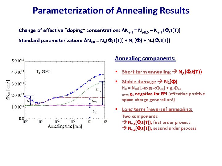
Parameterization of Annealing Results Change of effective “doping“ concentration: Neff = Neff, 0 – Neff ( , t(T)) Standard parameterization: Neff = NA( , t(T)) + NC( ) + NY( , t(T)) Annealing components: § Short term annealing NA( , t(T)) § Stable damage NC( ) NC = NC 0(1 -exp(-cΦeq) + g. CΦeq note: g. C negative for EPI (effective positive space charge generation!) § Long term (reverse) annealing: Two components: NY, 1( , t(T)), first order process NY, 2( , t(T)), second order process
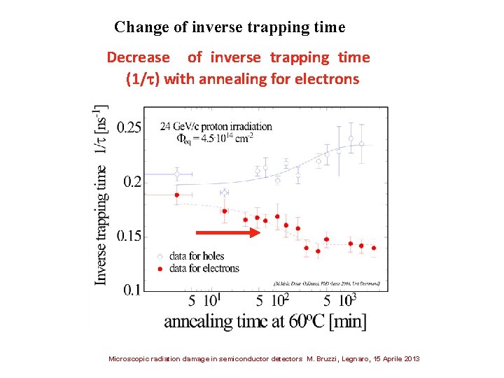
Change of inverse trapping time Decrease of inverse trapping time (1/ ) with annealing for electrons Microscopic radiation damage in semiconductor detectors M. Bruzzi, Legnaro, 15 Aprile 2013
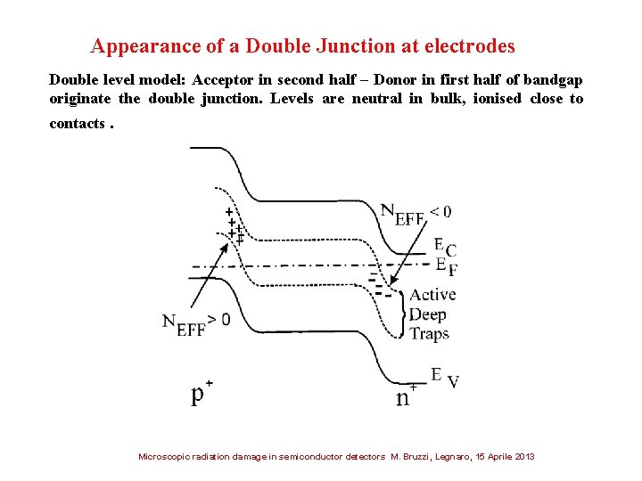
Appearance of a Double Junction at electrodes Double level model: Acceptor in second half – Donor in first half of bandgap originate the double junction. Levels are neutral in bulk, ionised close to contacts. Microscopic radiation damage in semiconductor detectors M. Bruzzi, Legnaro, 15 Aprile 2013
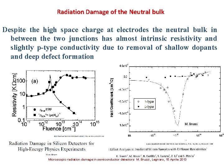
Radiation Damage of the Neutral bulk Despite the high space charge at electrodes the neutral bulk in between the two junctions has almost intrinsic resistivity and slightly p-type conductivity due to removal of shallow dopants and deep defect formation M. Bruzzi Microscopic radiation damage in semiconductor detectors M. Bruzzi, Legnaro, 15 Aprile 2013
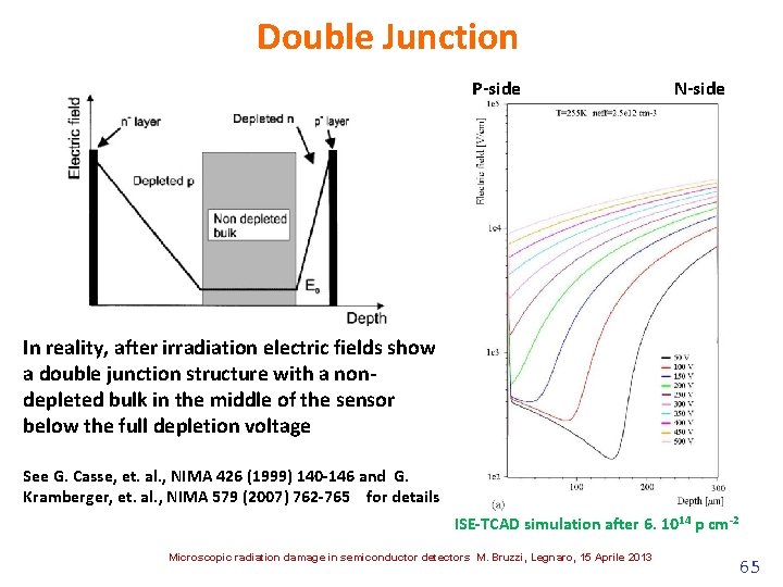
Double Junction P-side N-side In reality, after irradiation electric fields show a double junction structure with a nondepleted bulk in the middle of the sensor below the full depletion voltage See G. Casse, et. al. , NIMA 426 (1999) 140 -146 and G. Kramberger, et. al. , NIMA 579 (2007) 762 -765 for details ISE-TCAD simulation after 6. 1014 p cm-2 Microscopic radiation damage in semiconductor detectors M. Bruzzi, Legnaro, 15 Aprile 2013 65
Material Engineering Microscopic radiation damage in semiconductor detectors M. Bruzzi, Legnaro, 15 Aprile 2013
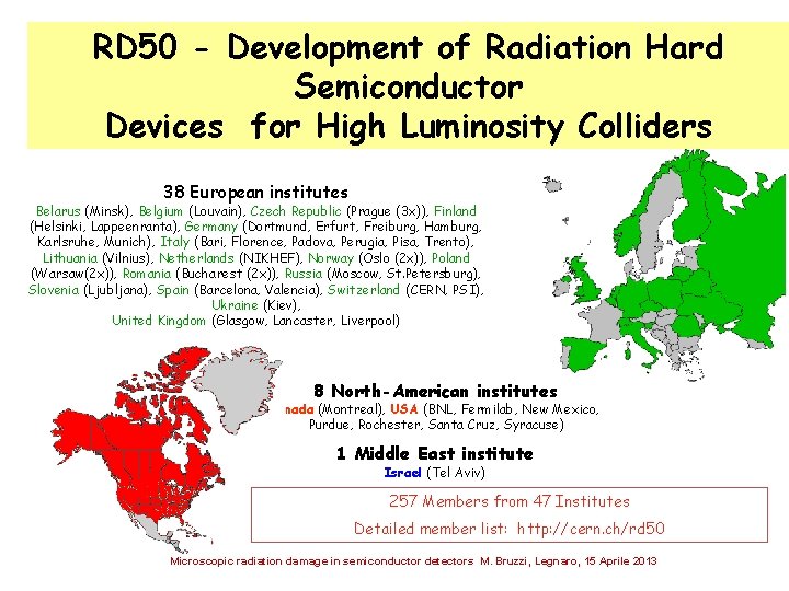
RD 50 - Development of Radiation Hard Semiconductor Devices for High Luminosity Colliders 38 European institutes Belarus (Minsk), Belgium (Louvain), Czech Republic (Prague (3 x)), Finland (Helsinki, Lappeenranta), Germany (Dortmund, Erfurt, Freiburg, Hamburg, Karlsruhe, Munich), Italy (Bari, Florence, Padova, Perugia, Pisa, Trento), Lithuania (Vilnius), Netherlands (NIKHEF), Norway (Oslo (2 x)), Poland (Warsaw(2 x)), Romania (Bucharest (2 x)), Russia (Moscow, St. Petersburg), Slovenia (Ljubljana), Spain (Barcelona, Valencia), Switzerland (CERN, PSI), Ukraine (Kiev), United Kingdom (Glasgow, Lancaster, Liverpool) 8 North-American institutes Canada (Montreal), USA (BNL, Fermilab, New Mexico, Purdue, Rochester, Santa Cruz, Syracuse) 1 Middle East institute Israel (Tel Aviv) 257 Members from 47 Institutes Detailed member list: http: //cern. ch/rd 50 Microscopic radiation damage in semiconductor detectors M. Bruzzi, Legnaro, 15 Aprile 2013
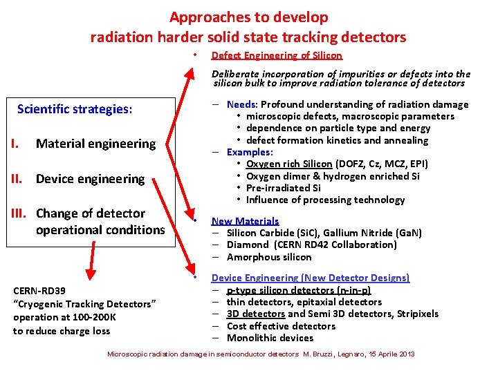
Approaches to develop radiation harder solid state tracking detectors • Defect Engineering of Silicon Deliberate incorporation of impurities or defects into the silicon bulk to improve radiation tolerance of detectors – Needs: Profound understanding of radiation damage • microscopic defects, macroscopic parameters • dependence on particle type and energy • defect formation kinetics and annealing – Examples: • Oxygen rich Silicon (DOFZ, Cz, MCZ, EPI) • Oxygen dimer & hydrogen enriched Si • Pre-irradiated Si • Influence of processing technology Scientific strategies: I. Material engineering II. Device engineering III. Change of detector operational conditions CERN-RD 39 “Cryogenic Tracking Detectors” operation at 100 -200 K to reduce charge loss • New Materials – Silicon Carbide (Si. C), Gallium Nitride (Ga. N) – Diamond (CERN RD 42 Collaboration) – Amorphous silicon • Device Engineering (New Detector Designs) – p-type silicon detectors (n-in-p) – thin detectors, epitaxial detectors – 3 D detectors and Semi 3 D detectors, Stripixels – Cost effective detectors – Monolithic devices Microscopic radiation damage in semiconductor detectors M. Bruzzi, Legnaro, 15 Aprile 2013
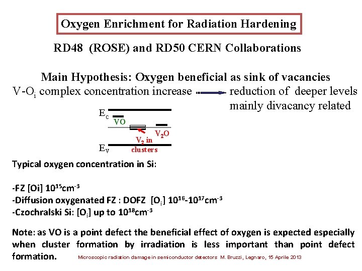
Oxygen Enrichment for Radiation Hardening RD 48 (ROSE) and RD 50 CERN Collaborations Main Hypothesis: Oxygen beneficial as sink of vacancies V-Oi complex concentration increase reduction of deeper levels mainly divacancy related Ec EV VO V 2 in clusters Typical oxygen concentration in Si: -FZ [Oi] 1015 cm-3 -Diffusion oxygenated FZ : DOFZ [Oi] 1016 -1017 cm-3 -Czochralski Si: [Oi] up to 1018 cm-3 Note: as VO is a point defect the beneficial effect of oxygen is expected especially when cluster formation by irradiation is less important than point defect Microscopic radiation damage in semiconductor detectors M. Bruzzi, Legnaro, 15 Aprile 2013 formation.
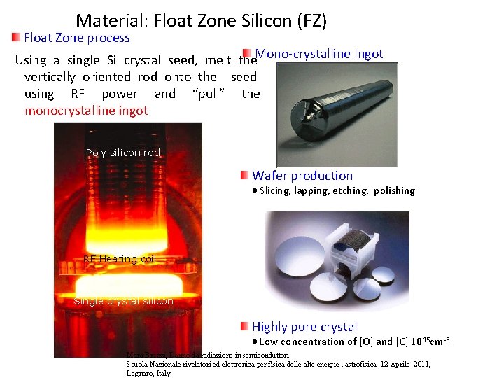
Material: Float Zone Silicon (FZ) Float Zone process Using a single Si crystal seed, melt the Mono-crystalline Ingot vertically oriented rod onto the seed using RF power and “pull” the monocrystalline ingot Poly silicon rod Wafer production Slicing, lapping, etching, polishing RF Heating coil Single crystal silicon Highly pure crystal Low concentration of [O] and [C] 1015 cm-3 Mara Bruzzi, Danno da radiazione in semiconduttori Scuola Nazionale rivelatori ed elettronica per fisica delle alte energie , astrofisica 12 Aprile 2011, Legnaro, Italy
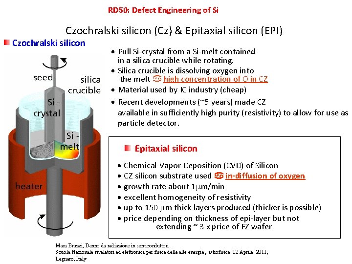
RD 50: Defect Engineering of Si Czochralski silicon (Cz) & Epitaxial silicon (EPI) Czochralski silicon Pull Si-crystal from a Si-melt contained in a silica crucible while rotating. Silica crucible is dissolving oxygen into the melt high concentration of O in CZ Material used by IC industry (cheap) Recent developments (~5 years) made CZ available in sufficiently high purity (resistivity) to allow for use as particle detector. Epitaxial silicon Chemical-Vapor Deposition (CVD) of Silicon CZ silicon substrate used in-diffusion of oxygen growth rate about 1 m/min excellent homogeneity of resistivity up to 150 m thick layers produced (thicker is possible) price depending on thickness of epi-layer but not extending ~ 3 x price of FZ wafer Mara Bruzzi, Danno da radiazione in semiconduttori Scuola Nazionale rivelatori ed elettronica per fisica delle alte energie , astrofisica 12 Aprile 2011, Legnaro, Italy
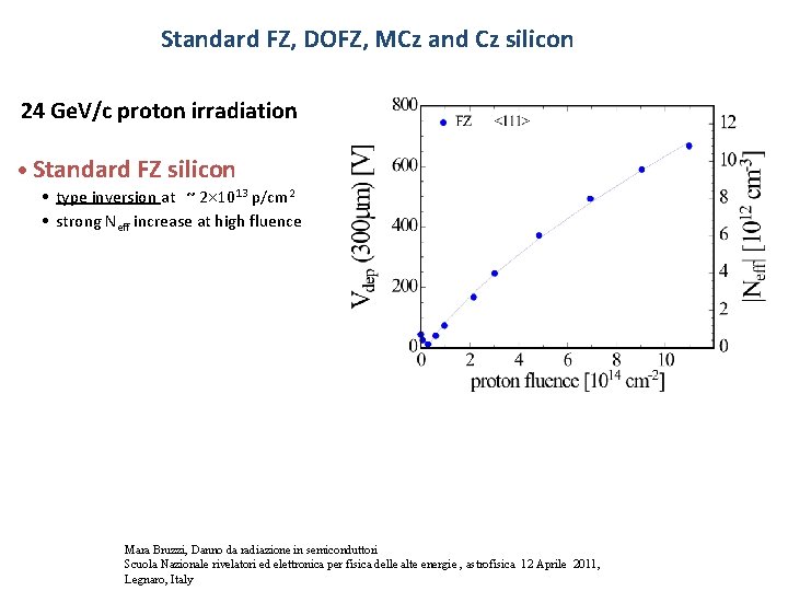
Standard FZ, DOFZ, MCz and Cz silicon 24 Ge. V/c proton irradiation Standard FZ silicon • type inversion at ~ 2 1013 p/cm 2 • strong Neff increase at high fluence Mara Bruzzi, Danno da radiazione in semiconduttori Scuola Nazionale rivelatori ed elettronica per fisica delle alte energie , astrofisica 12 Aprile 2011, Legnaro, Italy
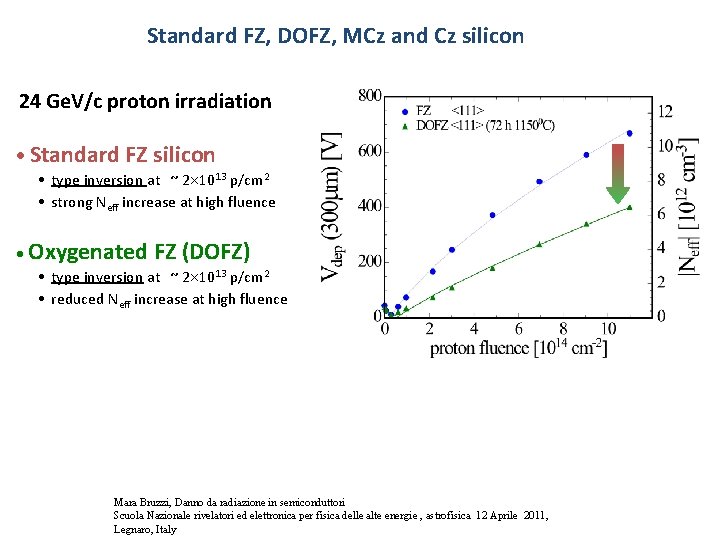
Standard FZ, DOFZ, MCz and Cz silicon 24 Ge. V/c proton irradiation Standard FZ silicon • type inversion at ~ 2 1013 p/cm 2 • strong Neff increase at high fluence Oxygenated FZ (DOFZ) • type inversion at ~ 2 1013 p/cm 2 • reduced Neff increase at high fluence Mara Bruzzi, Danno da radiazione in semiconduttori Scuola Nazionale rivelatori ed elettronica per fisica delle alte energie , astrofisica 12 Aprile 2011, Legnaro, Italy
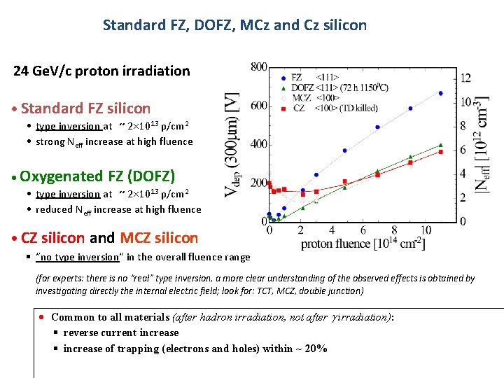
Standard FZ, DOFZ, MCz and Cz silicon 24 Ge. V/c proton irradiation Standard FZ silicon • type inversion at ~ 2 1013 p/cm 2 • strong Neff increase at high fluence Oxygenated FZ (DOFZ) • type inversion at ~ 2 1013 p/cm 2 • reduced Neff increase at high fluence CZ silicon and MCZ silicon § “no type inversion“ in the overall fluence range (for experts: there is no “real” type inversion, a more clear understanding of the observed effects is obtained by investigating directly the internal electric field; look for: TCT, MCZ, double junction) Common to all materials (after hadron irradiation, not after irradiation): § reverse current increase § increase of trapping (electrons and holes) within ~ 20%
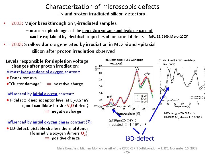
Characterization of microscopic defects - and proton irradiated silicon detectors - • 2003: Major breakthrough on -irradiated samples – macroscopic changes of the depletion voltage and leakage current can be explained by electrical properties of measured defects [APL, 82, 2169, March 2003] • 2005: Shallow donors generated by irradiation in MCz Si and epitaxial silicon after proton irradiation observed Levels responsible for depletion voltage changes after proton irradiation: [G. Lindstroem, RD 50 Workshop, Nov. . 2005] [D. Menichelli, RD 50 Workshop, Nov. . 2005] Almost independent of oxygen content: Donor removal “Cluster damage” negative charge Influenced by initial oxygen content: I–defect: deep acceptor level at EC-0. 54 e. V (good candidate for the V 2 O defect) negative charge Influenced by initial oxygen dimer content (? ): BD-defect: bistable shallow thermal donor (formed via oxygen dimers O 2 i) positive charge Epi 50 m 23 Ge. V p irradiated, F=4× 1014 cm-2 MCz n-type 26 Me. V p irradiated, F=4× 1014 cm-2 BD-defect Mara Bruzzi and Michael Moll on behalf of the RD 50 CERN Collaboration – LHCC, November 16, 2005 -75 -
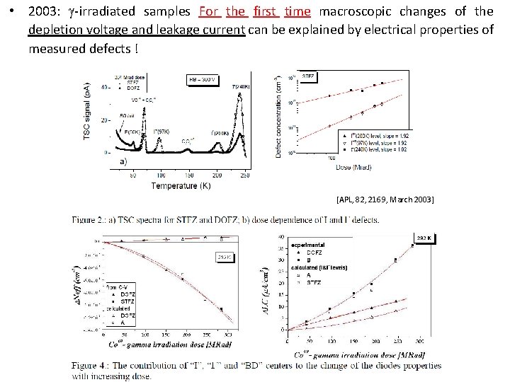
• 2003: -irradiated samples For the first time macroscopic changes of the depletion voltage and leakage current can be explained by electrical properties of measured defects ! [APL, 82, 2169, March 2003]
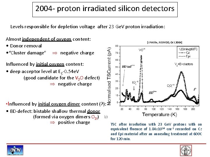
2004 - proton irradiated silicon detectors Levels responsible for depletion voltage after 23 Ge. V proton irradiation: Almost independent of oxygen content: • Donor removal • “Cluster damage” negative charge [I. Pintilie, RESMDD, Oct. 2004] Influenced by initial oxygen content: • deep acceptor level at EC-0. 54 e. V (good candidate for the V 2 O defect) negative charge • Influenced by initial oxygen dimer content (? ): • BD-defect: bistable shallow thermal donor (formed via oxygen dimers O 2 i) positive charge TSC after irradiation with 23 Ge. V protons with an equivalent fluence of 1. 84 x 1014 cm-2 recorded on Cz and Epi material after an annealing treatment at 600 C for 120 min.
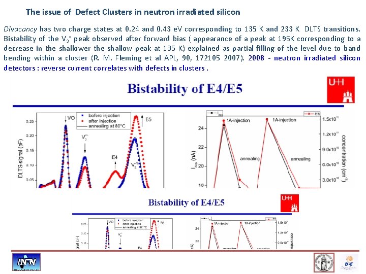
The issue of Defect Clusters in neutron irradiated silicon Divacancy has two charge states at 0. 24 and 0. 43 e. V corresponding to 135 K and 233 K DLTS transitions. Bistability of the V 2= peak observed after forward bias ( appearance of a peak at 195 K corresponding to a decrease in the shallower the shallow peak at 135 K) explained as partial filling of the level due to band bending within a cluster (R. M. Fleming et al APL, 90, 172105 2007). 2008 - neutron irradiated silicon detectors : reverse current correlates with defects in clusters.
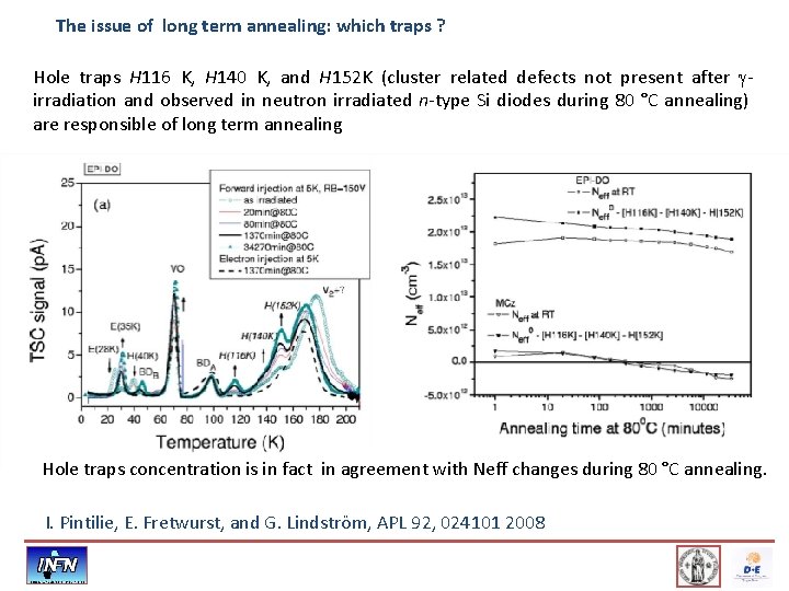
The issue of long term annealing: which traps ? Hole traps H 116 K, H 140 K, and H 152 K (cluster related defects not present after irradiation and observed in neutron irradiated n-type Si diodes during 80 °C annealing) are responsible of long term annealing Hole traps concentration is in fact in agreement with Neff changes during 80 °C annealing. I. Pintilie, E. Fretwurst, and G. Lindström, APL 92, 024101 2008
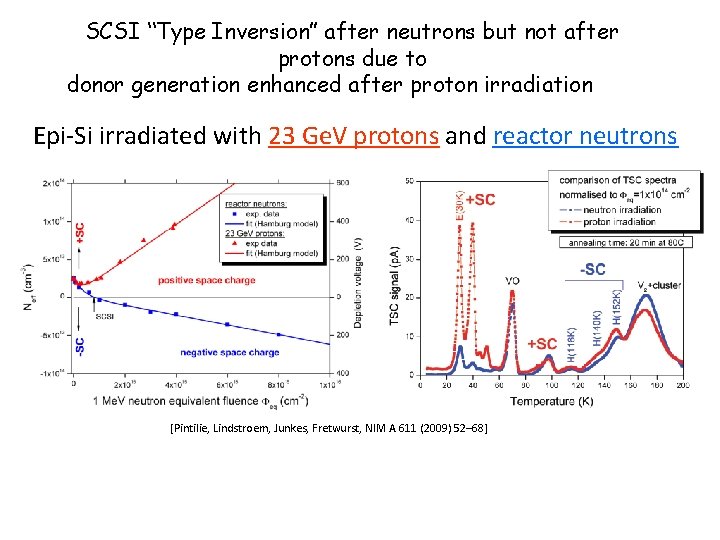
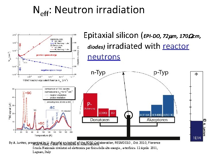
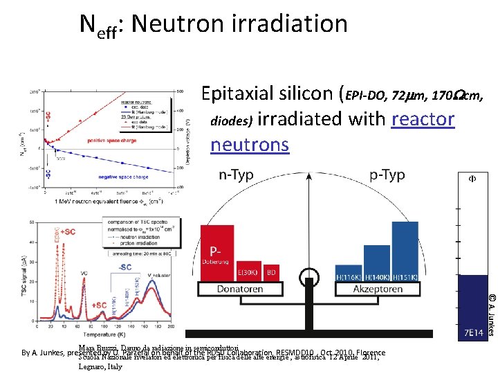
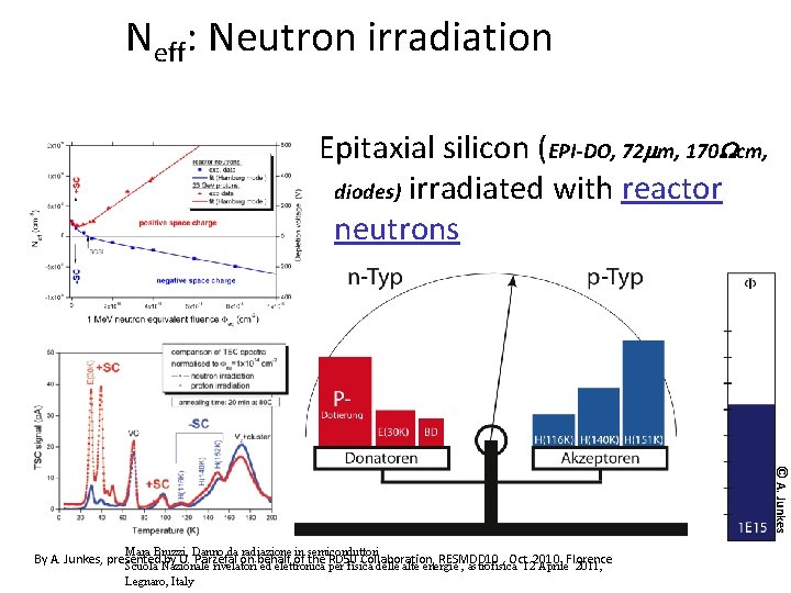
SCSI “Type Inversion” after neutrons but not after protons due to donor generation enhanced after proton irradiation Epi-Si irradiated with 23 Ge. V protons and reactor neutrons [Pintilie, Lindstroem, Junkes, Fretwurst, NIM A 611 (2009) 52– 68]
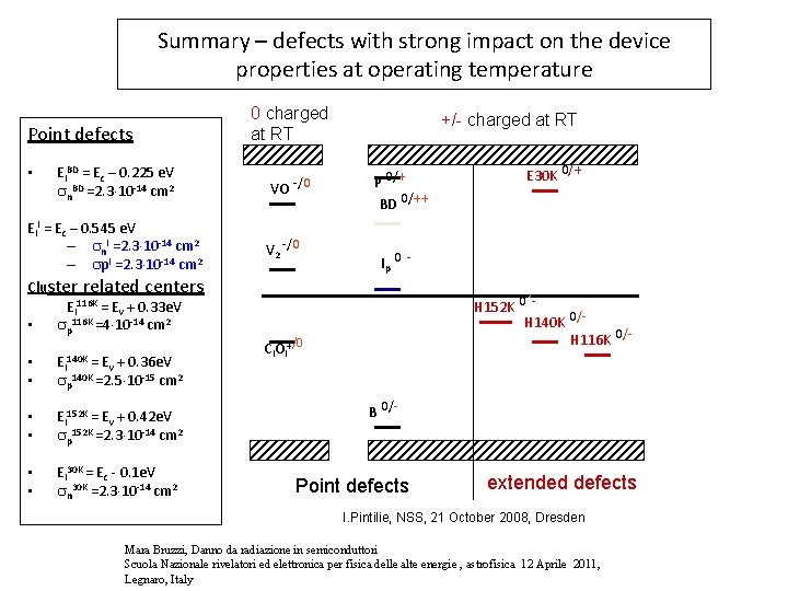
Summary – defects with strong impact on the device properties at operating temperature Point defects Ei. BD = Ec – 0. 225 e. V n. BD =2. 3 10 -14 cm 2 Ei. I = Ec – 0. 545 e. V – n. I =2. 3 10 -14 cm 2 – p. I =2. 3 10 -14 cm 2 Cluster related centers Ei 116 K = Ev + 0. 33 e. V • p 116 K =4 10 -14 cm 2 • • • Ei 140 K = Ev + 0. 36 e. V p 140 K =2. 5 10 -15 cm 2 • • Ei 152 K = Ev + 0. 42 e. V p 152 K =2. 3 10 -14 cm 2 • • Ei 30 K = Ec - 0. 1 e. V n 30 K =2. 3 10 -14 cm 2 0 charged at RT VO -/0 V 2 -/0 +/- charged at RT P 0/+ BD 0/++ E 30 K 0/+ Ip 0/H 152 K 0/H 140 K 0/H 116 K 0/- Ci. Oi+/0 B 0/- Point defects extended defects I. Pintilie, NSS, 21 October 2008, Dresden Mara Bruzzi, Danno da radiazione in semiconduttori Scuola Nazionale rivelatori ed elettronica per fisica delle alte energie , astrofisica 12 Aprile 2011, Legnaro, Italy
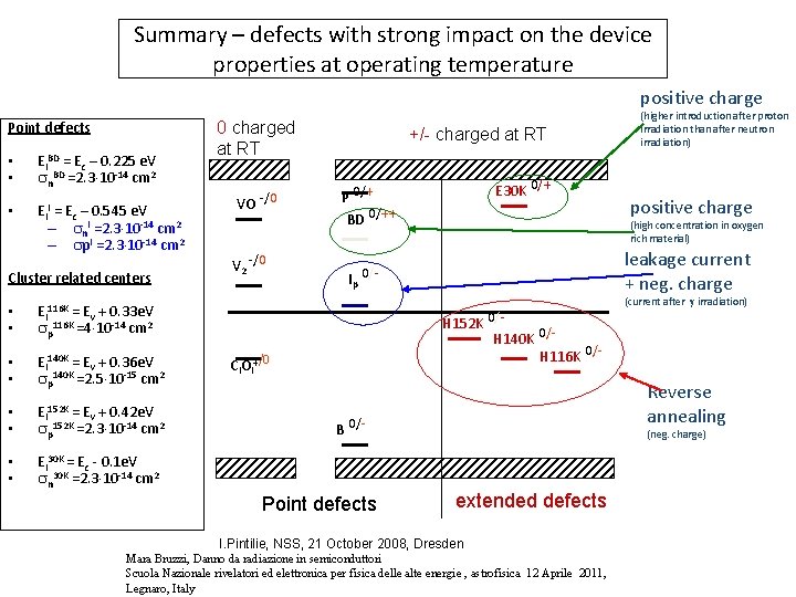
Summary – defects with strong impact on the device properties at operating temperature positive charge Point defects • • • Ei. BD = Ec – 0. 225 e. V n. BD =2. 3 10 -14 cm 2 Ei. I = Ec – 0. 545 e. V – n. I =2. 3 10 -14 cm 2 – p. I =2. 3 10 -14 cm 2 Cluster related centers • • Ei 116 K = Ev + 0. 33 e. V p 116 K =4 10 -14 cm 2 • • Ei 140 K = Ev + 0. 36 e. V p 140 K =2. 5 10 -15 cm 2 • • Ei 152 K = Ev + 0. 42 e. V p 152 K =2. 3 10 -14 cm 2 • • Ei 30 K = Ec - 0. 1 e. V n 30 K =2. 3 10 -14 cm 2 0 charged at RT VO -/0 V 2 -/0 +/- charged at RT E 30 K 0/+ P 0/+ BD 0/++ (higher introduction after proton irradiation than after neutron irradiation) positive charge (high concentration in oxygen rich material) leakage current + neg. charge Ip 0/- (current after irradiation) H 152 K 0/H 140 K 0/H 116 K 0/- Ci. Oi+/0 Reverse annealing B 0/- Point defects (neg. charge) extended defects I. Pintilie, NSS, 21 October 2008, Dresden Mara Bruzzi, Danno da radiazione in semiconduttori Scuola Nazionale rivelatori ed elettronica per fisica delle alte energie , astrofisica 12 Aprile 2011, Legnaro, Italy
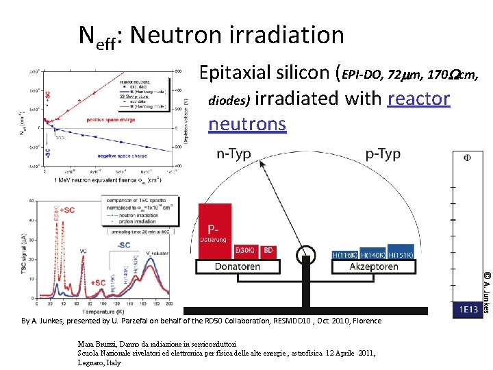
Neff: Neutron irradiation Epitaxial silicon (EPI-DO, 72 mm, 170 Wcm, diodes) irradiated with reactor neutrons © A. Junkes By A. Junkes, presented by U. Parzefal on behalf of the RD 50 Collaboration, RESMDD 10 , Oct. 2010, Florence Mara Bruzzi, Danno da radiazione in semiconduttori Scuola Nazionale rivelatori ed elettronica per fisica delle alte energie , astrofisica 12 Aprile 2011, Legnaro, Italy
Neff: Neutron irradiation Epitaxial silicon (EPI-DO, 72 mm, 170 Wcm, diodes) irradiated with reactor neutrons © A. Junkes By A. Junkes, presented by U. Parzefal on behalf of the RD 50 Collaboration, RESMDD 10 , Oct. 2010, Florence Mara Bruzzi, Danno da radiazione in semiconduttori Scuola Nazionale rivelatori ed elettronica per fisica delle alte energie , astrofisica 12 Aprile 2011, Legnaro, Italy
Neff: Neutron irradiation Epitaxial silicon (EPI-DO, 72 mm, 170 Wcm, diodes) irradiated with reactor neutrons © A. Junkes Mara Bruzzi, Danno da radiazione in semiconduttori Scuola Nazionale rivelatori ed elettronica per fisica delle alte energie , astrofisica 12 Aprile 2011, Legnaro, Italy By A. Junkes, presented by U. Parzefal on behalf of the RD 50 Collaboration, RESMDD 10 , Oct. 2010, Florence
Neff: Neutron irradiation Epitaxial silicon (EPI-DO, 72 mm, 170 Wcm, diodes) irradiated with reactor neutrons © A. Junkes Mara Bruzzi, Danno da radiazione in semiconduttori Scuola Nazionale rivelatori ed elettronica per fisica delle alte energie , astrofisica 12 Aprile 2011, Legnaro, Italy By A. Junkes, presented by U. Parzefal on behalf of the RD 50 Collaboration, RESMDD 10 , Oct. 2010, Florence
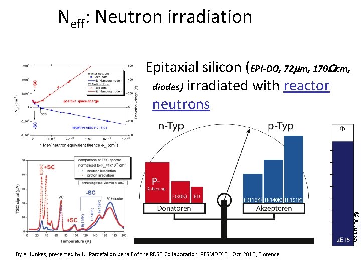
Neff: Neutron irradiation Epitaxial silicon (EPI-DO, 72 mm, 170 Wcm, diodes) irradiated with reactor neutrons © A. Junkes By A. Junkes, presented by U. Parzefal on behalf of the RD 50 Collaboration, RESMDD 10 , Oct. 2010, Florence
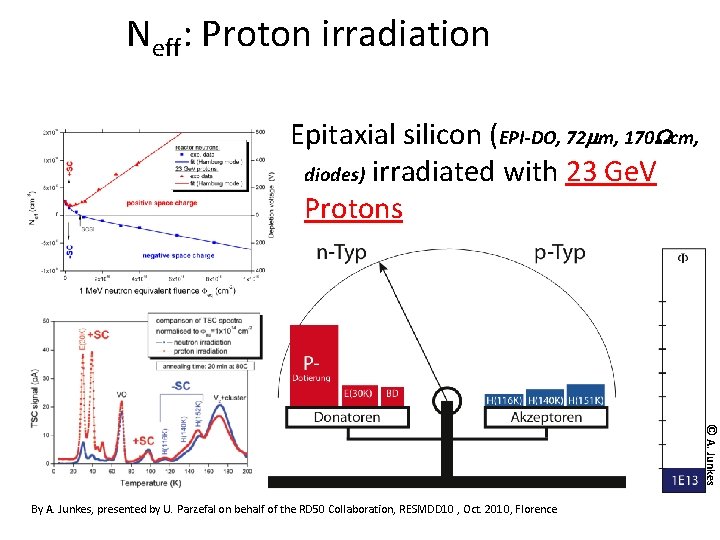
Neff: Proton irradiation Epitaxial silicon (EPI-DO, 72 mm, 170 Wcm, diodes) irradiated with 23 Ge. V Protons © A. Junkes By A. Junkes, presented by U. Parzefal on behalf of the RD 50 Collaboration, RESMDD 10 , Oct. 2010, Florence
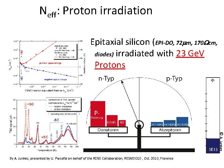
Neff: Proton irradiation Epitaxial silicon (EPI-DO, 72 mm, 170 Wcm, diodes) irradiated with 23 Ge. V Protons © A. Junkes By A. Junkes, presented by U. Parzefal on behalf of the RD 50 Collaboration, RESMDD 10 , Oct. 2010, Florence
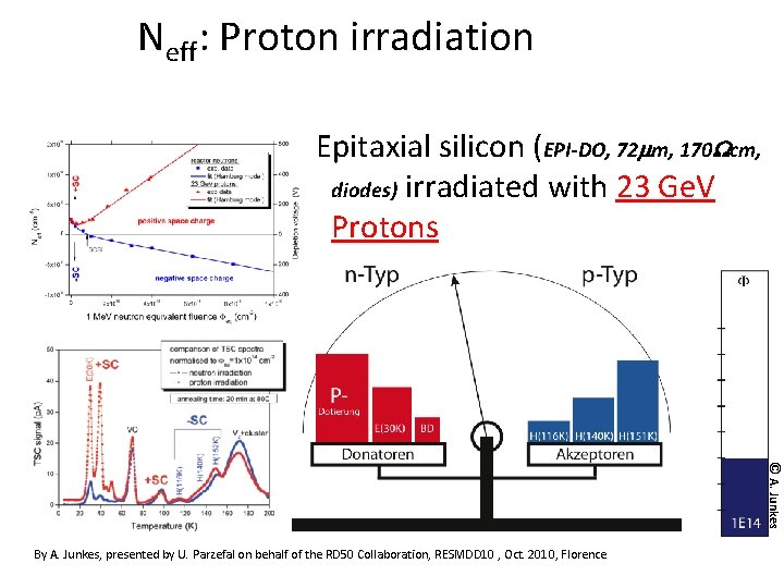
Neff: Proton irradiation Epitaxial silicon (EPI-DO, 72 mm, 170 Wcm, diodes) irradiated with 23 Ge. V Protons © A. Junkes By A. Junkes, presented by U. Parzefal on behalf of the RD 50 Collaboration, RESMDD 10 , Oct. 2010, Florence
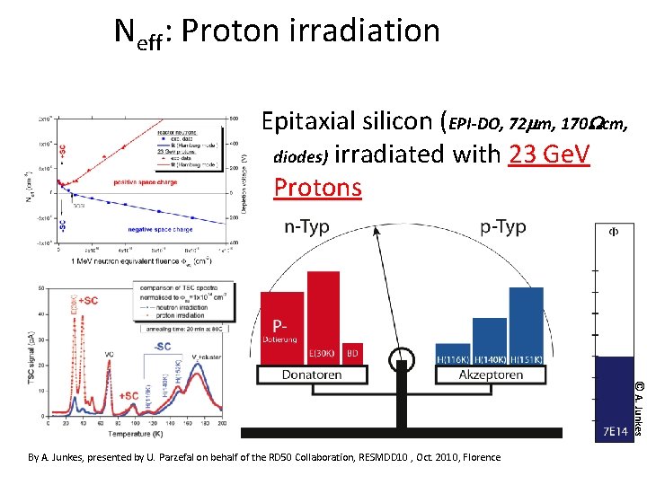
Neff: Proton irradiation Epitaxial silicon (EPI-DO, 72 mm, 170 Wcm, diodes) irradiated with 23 Ge. V Protons © A. Junkes By A. Junkes, presented by U. Parzefal on behalf of the RD 50 Collaboration, RESMDD 10 , Oct. 2010, Florence
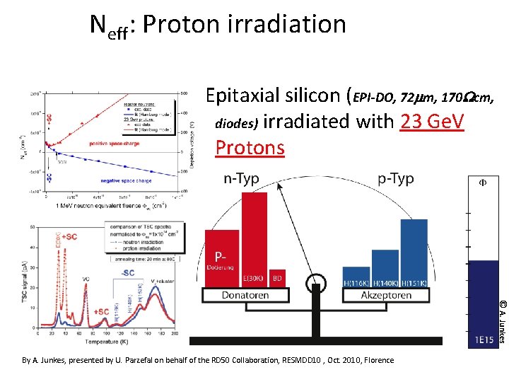
Neff: Proton irradiation Epitaxial silicon (EPI-DO, 72 mm, 170 Wcm, diodes) irradiated with 23 Ge. V Protons © A. Junkes By A. Junkes, presented by U. Parzefal on behalf of the RD 50 Collaboration, RESMDD 10 , Oct. 2010, Florence
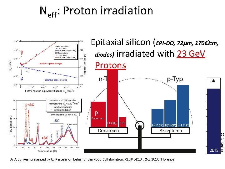
Neff: Proton irradiation Epitaxial silicon (EPI-DO, 72 mm, 170 Wcm, diodes) irradiated with 23 Ge. V Protons © A. Junkes By A. Junkes, presented by U. Parzefal on behalf of the RD 50 Collaboration, RESMDD 10 , Oct. 2010, Florence
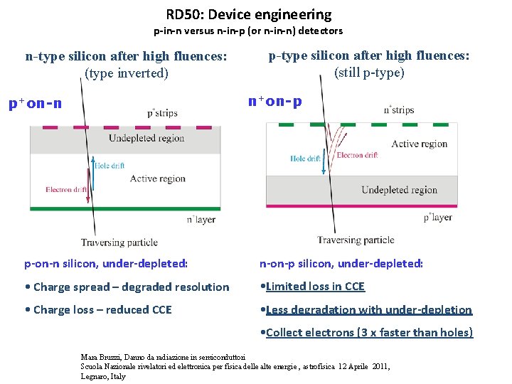
RD 50: Device engineering p-in-n versus n-in-p (or n-in-n) detectors n-type silicon after high fluences: (type inverted) p-type silicon after high fluences: (still p-type) n+on-p p+on-n p-on-n silicon, under-depleted: n-on-p silicon, under-depleted: • Charge spread – degraded resolution • Limited loss in CCE • Charge loss – reduced CCE • Less degradation with under-depletion • Collect electrons (3 x faster than holes) Mara Bruzzi, Danno da radiazione in semiconduttori Scuola Nazionale rivelatori ed elettronica per fisica delle alte energie , astrofisica 12 Aprile 2011, Legnaro, Italy
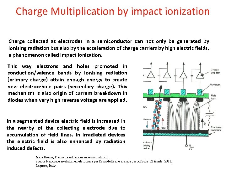
Charge Multiplication by impact ionization Charge collected at electrodes in a semiconductor can not only be generated by ionising radiation but also by the acceleration of charge carriers by high electric fields, a phenomenon called impact ionization. This way electrons and holes promoted in conduction/valence bands by ionising radiation (primary charge) attain enough energy to create new electron-hole pairs (secondary charge). This mechanism is also origin of current breakdown in diodes when very high reverse voltage are applied. In a segmented device electric field is increased in the nearby of the collecting electrode due to accumulation of field lines. In irradiated devices the electric field is also enhanced by radiation induced defects. Mara Bruzzi, Danno da radiazione in semiconduttori Scuola Nazionale rivelatori ed elettronica per fisica delle alte energie , astrofisica 12 Aprile 2011, Legnaro, Italy
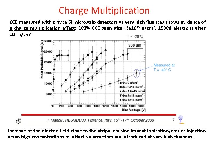
Charge Multiplication CCE measured with p-type Si microstrip detectors at very high fluences shows evidence of a charge multiplication effect: 100% CCE seen after 3 x 10¹⁵ n/cm 2, 15000 electrons after 1016 n/cm 2 Increase of the electric field close to the strips causing impact ionization/carrier injection when high concentrations of effective acceptors are introduced at very high fluences.
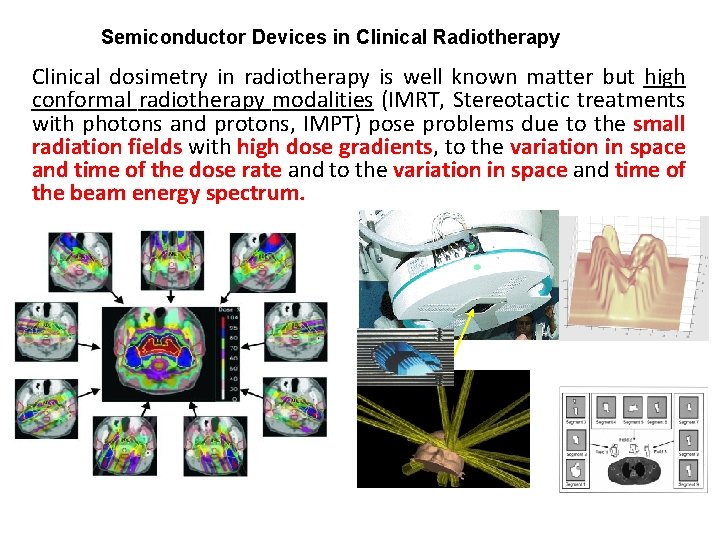
Semiconductor Devices in Clinical Radiotherapy Clinical dosimetry in radiotherapy is well known matter but high conformal radiotherapy modalities (IMRT, Stereotactic treatments with photons and protons, IMPT) pose problems due to the small radiation fields with high dose gradients, to the variation in space and time of the dose rate and to the variation in space and time of the beam energy spectrum.
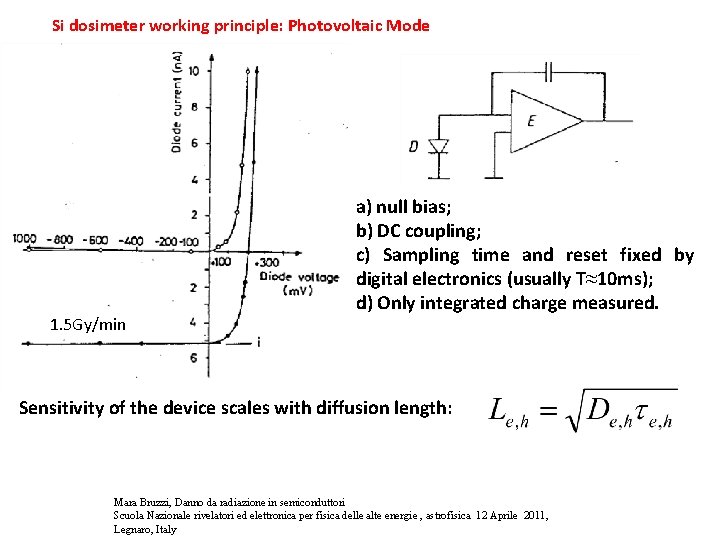
Si dosimeter working principle: Photovoltaic Mode 1. 5 Gy/min a) null bias; b) DC coupling; c) Sampling time and reset fixed by digital electronics (usually T≈10 ms); d) Only integrated charge measured. Sensitivity of the device scales with diffusion length: Mara Bruzzi, Danno da radiazione in semiconduttori Scuola Nazionale rivelatori ed elettronica per fisica delle alte energie , astrofisica 12 Aprile 2011, Legnaro, Italy
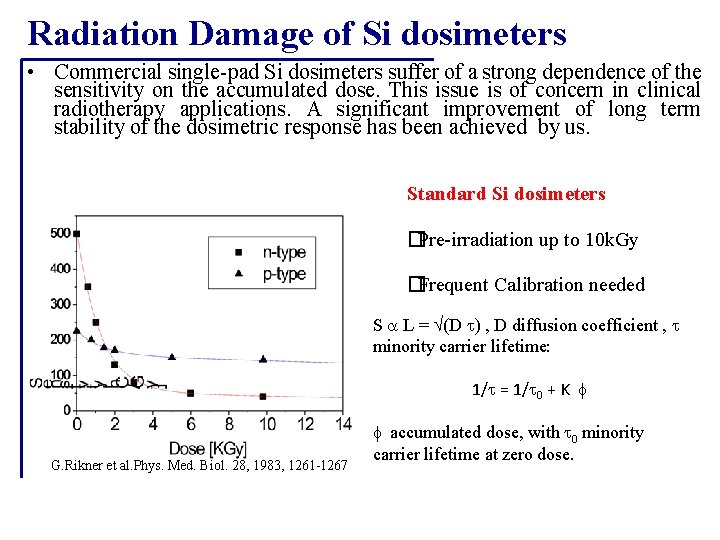
Radiation Damage of Si dosimeters • Commercial single-pad Si dosimeters suffer of a strong dependence of the sensitivity on the accumulated dose. This issue is of concern in clinical radiotherapy applications. A significant improvement of long term stability of the dosimetric response has been achieved by us. Standard Si dosimeters �Pre-irradiation up to 10 k. Gy �Frequent Calibration needed S a L = (D ) , D diffusion coefficient , minority carrier lifetime: 1/ = 1/ 0 + K f G. Rikner et al. Phys. Med. Biol. 28, 1983, 1261 -1267 f accumulated dose, with 0 minority carrier lifetime at zero dose.
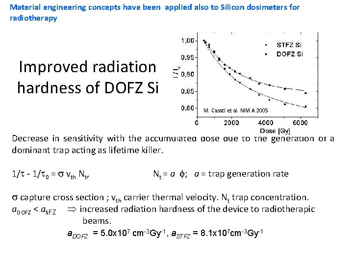
Material engineering concepts have been applied also to Silicon dosimeters for radiotherapy Improved radiation hardness of DOFZ Si M. Casati et al. NIM A 2005 Decrease in sensitivity with the accumulated dose due to the generation of a dominant trap acting as lifetime killer. 1/ - 1/ 0 = vth Nt, Nt = a f; a = trap generation rate capture cross section ; vth carrier thermal velocity. Nt trap concentration. a. DOFZ < a. SFZ increased radiation hardness of the device to radiotherapic beams. a. DOFZ = 5. 0 x 107 cm-3 Gy-1, a. STFZ = 8. 1 x 107 cm-3 Gy-1
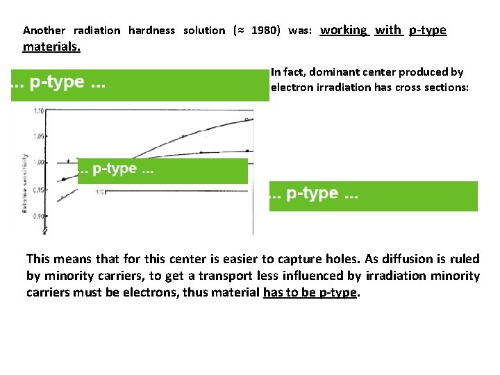
Another radiation hardness solution (≈ 1980) was: working with p-type materials. In fact, dominant center produced by electron irradiation has cross sections: This means that for this center is easier to capture holes. As diffusion is ruled by minority carriers, to get a transport less influenced by irradiation minority carriers must be electrons, thus material has to be p-type.
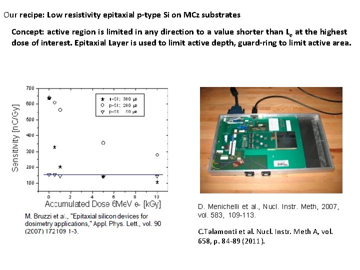
Our recipe: Low resistivity epitaxial p-type Si on MCz substrates Concept: active region is limited in any direction to a value shorter than Le at the highest dose of interest. Epitaxial Layer is used to limit active depth, guard-ring to limit active area. D. Menichelli et al. , Nucl. Instr. Meth, 2007, vol. 583, 109 -113. C. Talamonti et al. Nucl. Instr. Meth A, vol. 658, p. 84 -89 (2011).
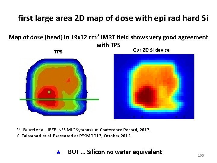
first large area 2 D map of dose with epi rad hard Si Map of dose (head) in 19 x 12 cm 2 IMRT field shows very good agreement with TPS Our 2 D Si device M. Bruzzi et al. , IEEE NSS MIC Symposium Conference Record, 2012. C. Talamonti et al. Presented at RESMDD 12, October 2012. BUT … Silicon no water equivalent 103
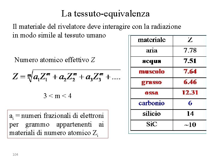
La tessuto-equivalenza Il materiale del rivelatore deve interagire con la radiazione in modo simile al tessuto umano Numero atomico effettivo Z 3<m<4 ai = numeri frazionali di elettroni per grammo appartenenti ai materiali di numero atomico Zi 104
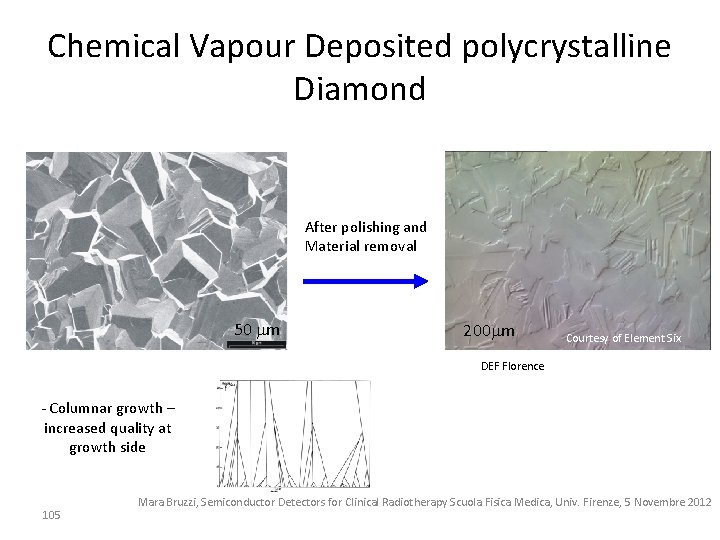
Chemical Vapour Deposited polycrystalline Diamond After polishing and Material removal 50 m 200 m Courtesy of Element Six DEF Florence - Columnar growth – increased quality at growth side 105 Mara Bruzzi, Semiconductor Detectors for Clinical Radiotherapy Scuola Fisica Medica, Univ. Firenze, 5 Novembre 2012
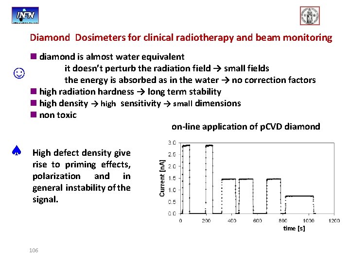
Diamond Dosimeters for clinical radiotherapy and beam monitoring ☺ n diamond is almost water equivalent it doesn’t perturb the radiation field → small fields the energy is absorbed as in the water → no correction factors n high radiation hardness → long term stability n high density → high sensitivity → small dimensions n non toxic on-line application of p. CVD diamond High defect density give rise to priming effects, polarization and in general instability of the signal. 106
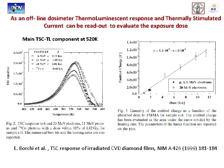
As an off- line dosimeter Thermo. Luminescent response and Thermally Stimulated Current can be read-out to evaluate the exposure dose Main TSC-TL component at 520 K E. Borchi et al. , TSC response of irradiated CVD diamond films, NIM A 426 (1999) 181 -184
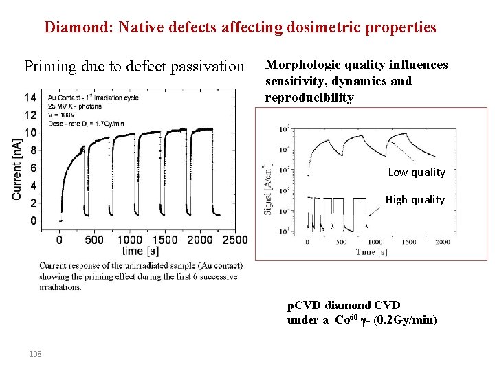
Diamond: Native defects affecting dosimetric properties Priming due to defect passivation Morphologic quality influences sensitivity, dynamics and reproducibility Low quality High quality p. CVD diamond CVD under a Co 60 g- (0. 2 Gy/min) 108
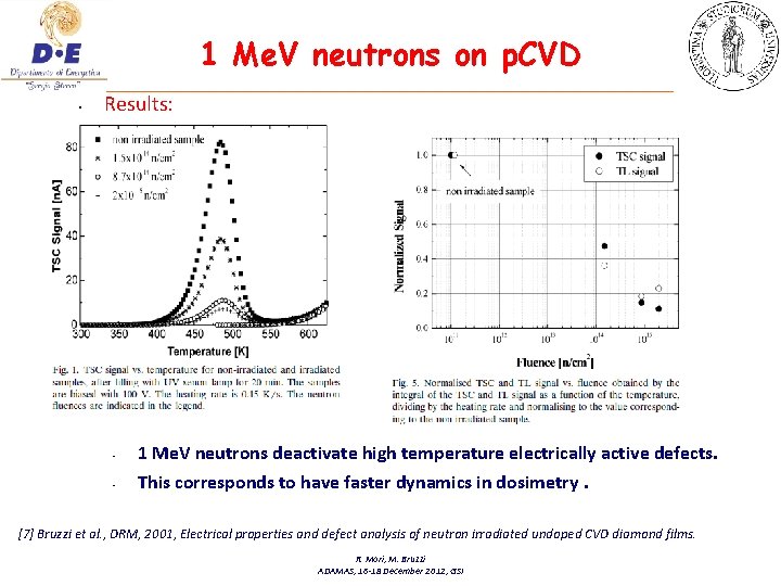
1 Me. V neutrons on p. CVD • Results: • 1 Me. V neutrons deactivate high temperature electrically active defects. • This corresponds to have faster dynamics in dosimetry. [7] Bruzzi et al. , DRM, 2001, Electrical properties and defect analysis of neutron irradiated undoped CVD diamond films. R. Mori, M. Bruzzi ADAMAS, 16 -18 December 2012, GSI
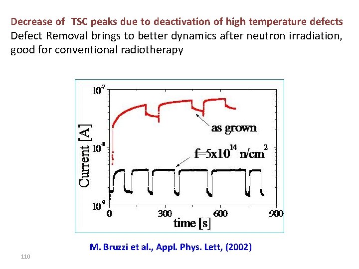
Decrease of TSC peaks due to deactivation of high temperature defects Defect Removal brings to better dynamics after neutron irradiation, good for conventional radiotherapy M. Bruzzi et al. , Appl. Phys. Lett, (2002) 110
Conclusions • Microscopic view of radiation Damage is a useful tool to quantitatively explain macroscopic radiation damage in semiconductor devices • Material/Device Enginering successful • Best to work on the subject interdisciplinarly • RD 50 forum for development of Ultra Radiation Hard Semiconductor Detectors • Performance can improve after irradiation (see diamond dosimeters) due to passivation of native defects.
- Slides: 111