MICROPROCESSOR SYSTEMS Week6 INTERFACING Semiconductor Memory Types Memory

- Slides: 40

MICROPROCESSOR SYSTEMS Week-6 INTERFACING

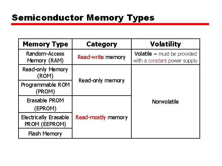
Semiconductor Memory Types Memory Type Category Random-Access Memory (RAM) Read-write memory Read-only Memory (ROM) Programmable ROM (PROM) Flash Memory Volatile – must be provided with a constant power supply Read-only memory Erasable PROM (EPROM) Electrically Erasable PROM (EEPROM) Volatility Nonvolatile Read-mostly memory

Semiconductor Memory • RAM —Misnamed as all semiconductor memory is random access (as all of the types listed in the previous table) —Read/Write —Volatile —Temporary storage

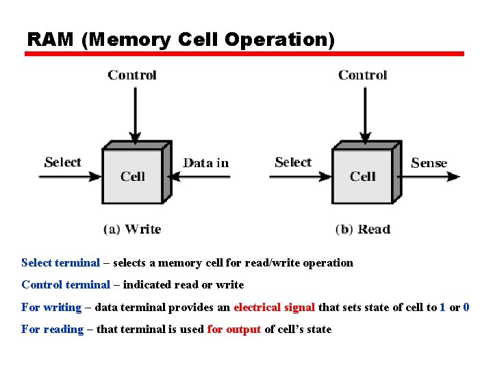
RAM (Memory Cell Operation) Select terminal – selects a memory cell for read/write operation Control terminal – indicated read or write For writing – data terminal provides an electrical signal that sets state of cell to 1 or 0 For reading – that terminal is used for output of cell’s state

Semiconductor Memory ØRAM technology is divided into two technologies: — Dynamic and Static

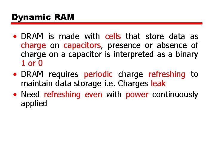
Dynamic RAM • DRAM is made with cells that store data as charge on capacitors, presence or absence of charge on a capacitor is interpreted as a binary 1 or 0 • DRAM requires periodic charge refreshing to maintain data storage i. e. Charges leak • Need refreshing even with power continuously applied

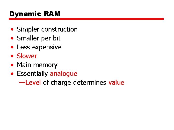
Dynamic RAM • • • Simpler construction Smaller per bit Less expensive Slower Main memory Essentially analogue —Level of charge determines value

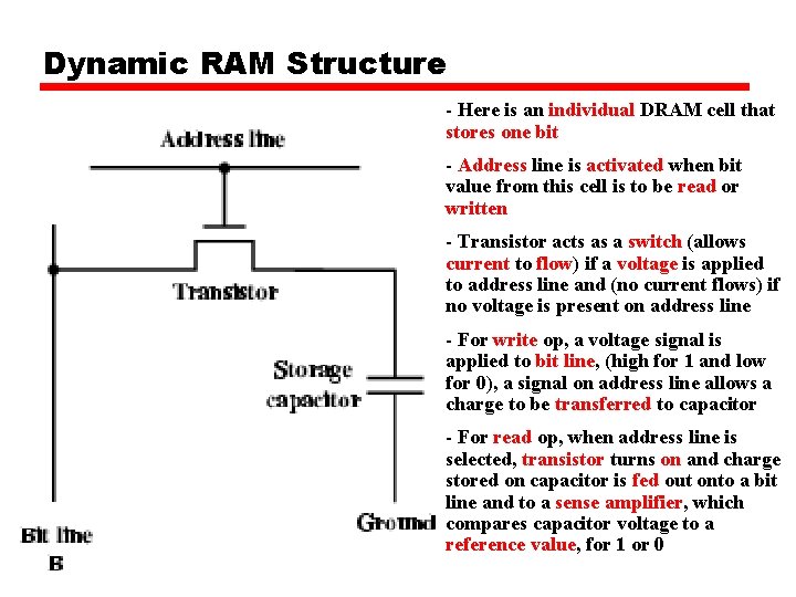
Dynamic RAM Structure - Here is an individual DRAM cell that stores one bit - Address line is activated when bit value from this cell is to be read or written - Transistor acts as a switch (allows current to flow) if a voltage is applied to address line and (no current flows) if no voltage is present on address line - For write op, a voltage signal is applied to bit line, (high for 1 and low for 0), a signal on address line allows a charge to be transferred to capacitor - For read op, when address line is selected, transistor turns on and charge stored on capacitor is fed out onto a bit line and to a sense amplifier, which compares capacitor voltage to a reference value, for 1 or 0

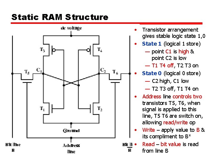
Static RAM Structure • • • Transistor arrangement gives stable logic state 1, 0 State 1 (logical 1 store) — point C 1 is high & point C 2 is low — T 1 T 4 off, T 2 T 3 on State 0 (logical 0 store) — C 2 high, C 1 low — T 2 T 3 off, T 1 T 4 on Address line controls two transistors T 5, T 6, when signal is applied to this line, T 5 T 6 are switch on, allowing read/write op Write – apply value to B & its compliment to B* Read – bit value is read from line B

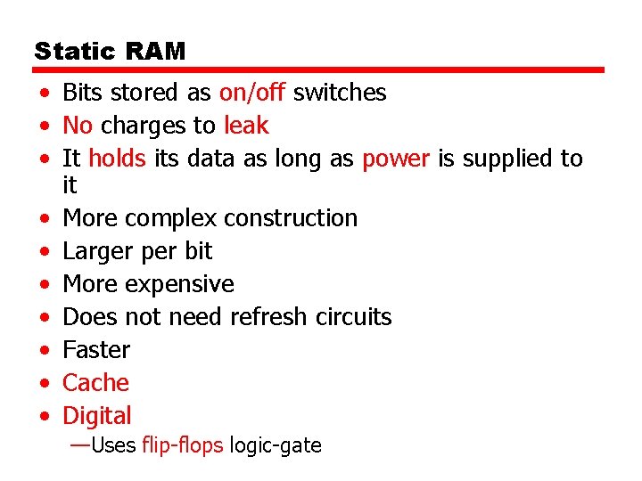
Static RAM • Bits stored as on/off switches • No charges to leak • It holds its data as long as power is supplied to it • More complex construction • Larger per bit • More expensive • Does not need refresh circuits • Faster • Cache • Digital —Uses flip-flops logic-gate

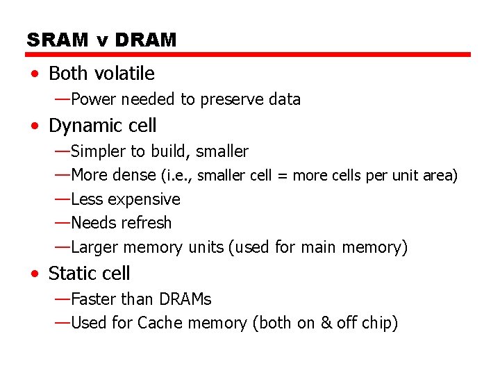
SRAM v DRAM • Both volatile —Power needed to preserve data • Dynamic cell —Simpler to build, smaller —More dense (i. e. , smaller cell = more cells per unit area) —Less expensive —Needs refresh —Larger memory units (used for main memory) • Static cell —Faster than DRAMs —Used for Cache memory (both on & off chip)

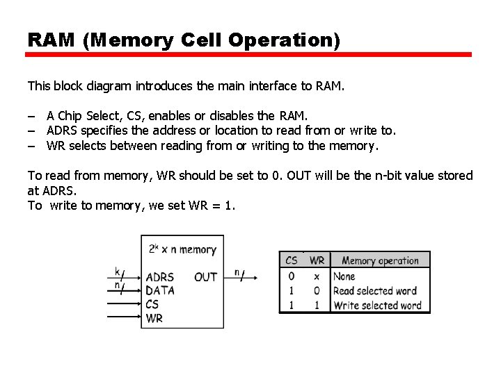
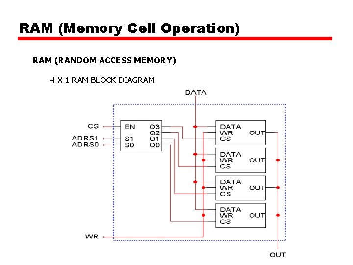
RAM (Memory Cell Operation) This block diagram introduces the main interface to RAM. – A Chip Select, CS, enables or disables the RAM. – ADRS specifies the address or location to read from or write to. – WR selects between reading from or writing to the memory. To read from memory, WR should be set to 0. OUT will be the n-bit value stored at ADRS. To write to memory, we set WR = 1.

RAM (Memory Cell Operation) RAM (RANDOM ACCESS MEMORY) 4 X 1 RAM BLOCK DIAGRAM

Read Only Memory (ROM) • Permanent storage —Nonvolatile • • Microprogramming Library subroutines Systems programs (BIOS) Function tables

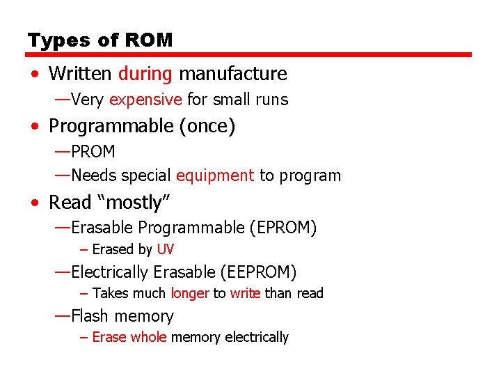
Types of ROM • Written during manufacture —Very expensive for small runs • Programmable (once) —PROM —Needs special equipment to program • Read “mostly” —Erasable Programmable (EPROM) – Erased by UV —Electrically Erasable (EEPROM) – Takes much longer to write than read —Flash memory – Erase whole memory electrically

Semiconductor Memory Types PROM Small, written only once, special equipment is required for programming Ø In read-mostly-memory, the Read op are far more frequent than write op EPROM All storage cells must be erased to same initial state by an ultraviolet light, it takes 20 min to perform, can be used multiple times

Semiconductor Memory Types EEPROM That can be written into at any time without erasing prior contents; only byte or bytes addressed are updated. Write op takes longer time than read op, 100 µsec/byte. FLASH MEMORY Ø Kind of Non-volatile random-access memory Ø Slower than RAM but faster than hard drives

INTERFACING MEMORY WITH 8085 Ø Programs and data that are executed by the microprocessor have to be stored in ROM/EPROM and RAM Ø 8085 has 16 address lines (A 0 A 15) Maximum of 64 KB (= 2^16 bytes) of memory locations can be interfaced Ø Memory address space takes values from 0000 H to FFFFH Ø IO/M , RD and WR when it wants to read from and write into memory or I/O devices

INTERFACING MEMORY WITH 8085 Ø CE or CS(chip enable or chip select) Ø OE or RD (output enable or read) Ø WE or WR (write enable or write)

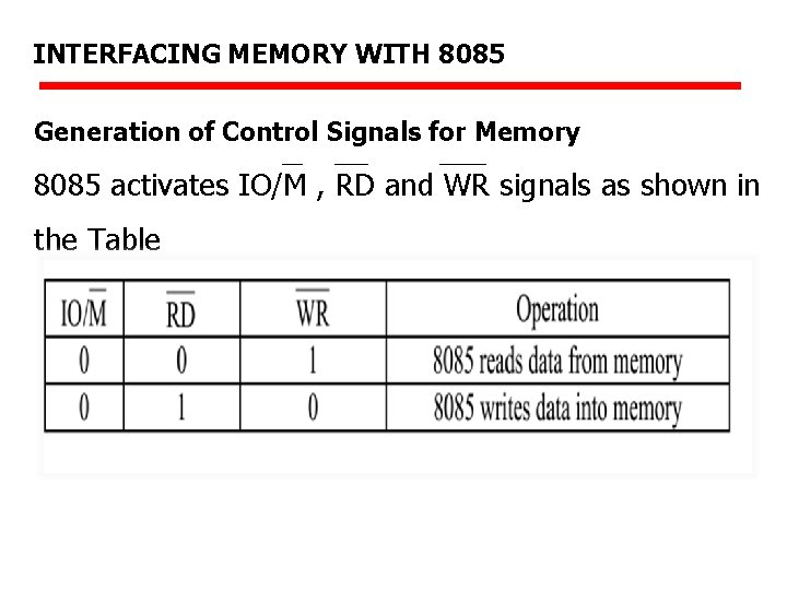
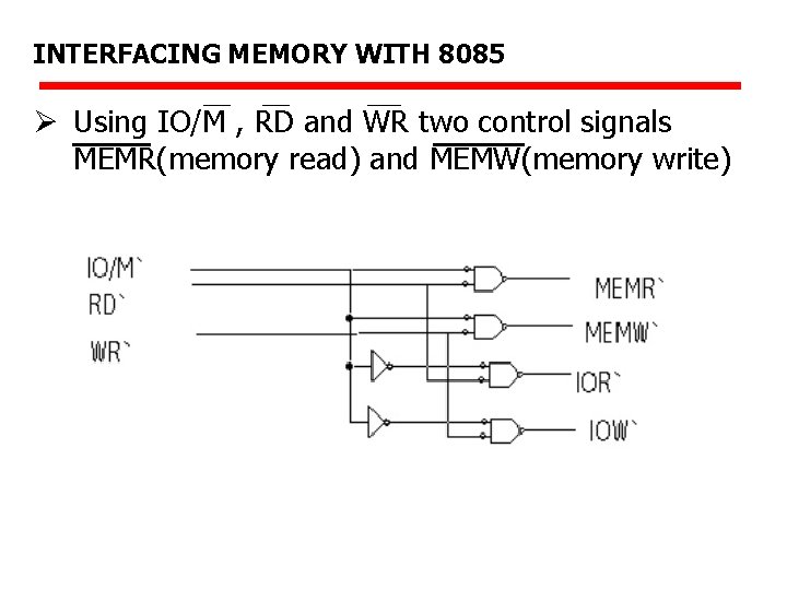
INTERFACING MEMORY WITH 8085 Generation of Control Signals for Memory 8085 activates IO/M , RD and WR signals as shown in the Table

INTERFACING MEMORY WITH 8085 Ø Using IO/M , RD and WR two control signals MEMR(memory read) and MEMW(memory write)

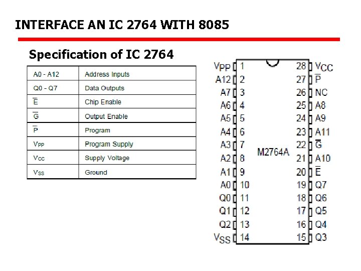
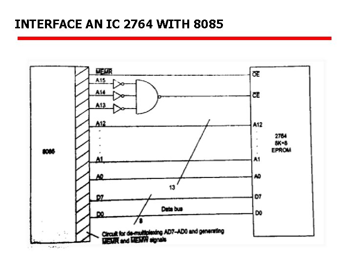
INTERFACE AN IC 2764 WITH 8085 Specification of IC 2764

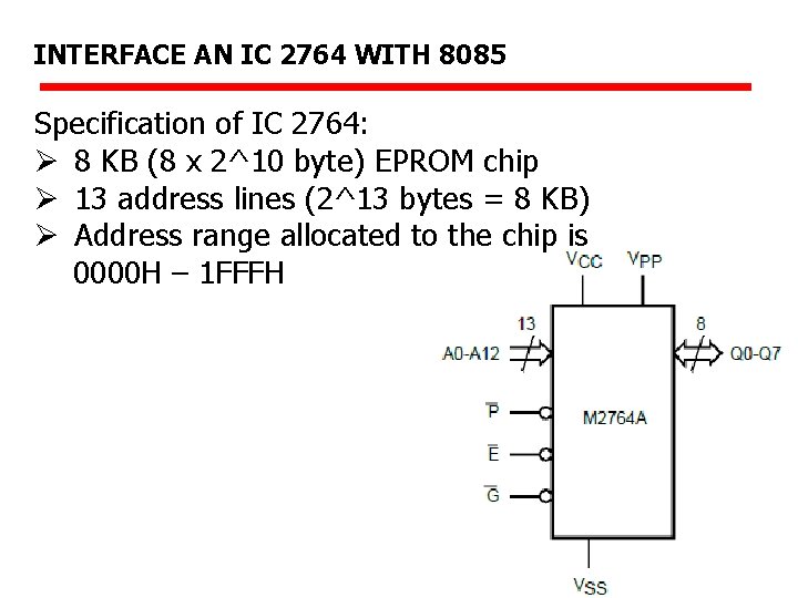
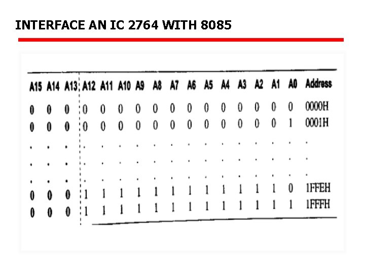
INTERFACE AN IC 2764 WITH 8085 Specification of IC 2764: Ø 8 KB (8 x 2^10 byte) EPROM chip Ø 13 address lines (2^13 bytes = 8 KB) Ø Address range allocated to the chip is 0000 H – 1 FFFH

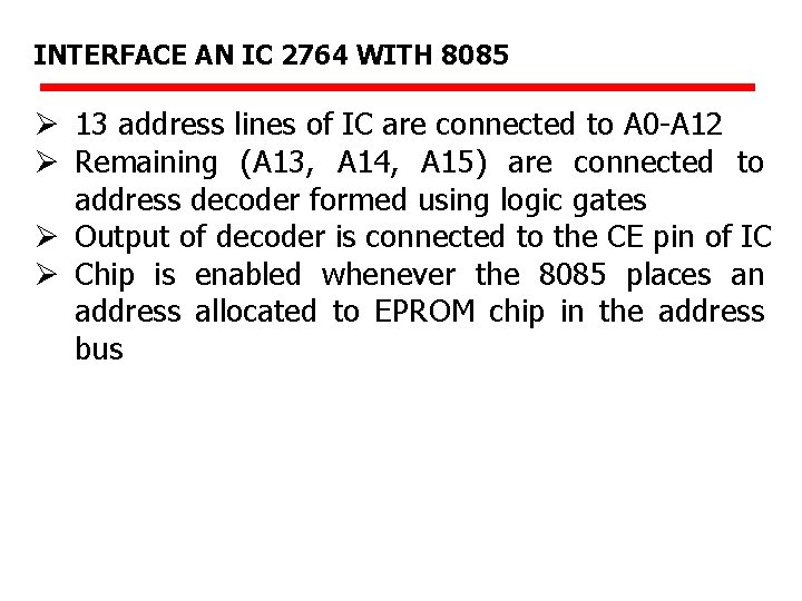
INTERFACE AN IC 2764 WITH 8085 Ø 13 address lines of IC are connected to A 0 -A 12 Ø Remaining (A 13, A 14, A 15) are connected to address decoder formed using logic gates Ø Output of decoder is connected to the CE pin of IC Ø Chip is enabled whenever the 8085 places an address allocated to EPROM chip in the address bus

INTERFACE AN IC 2764 WITH 8085

INTERFACE AN IC 2764 WITH 8085

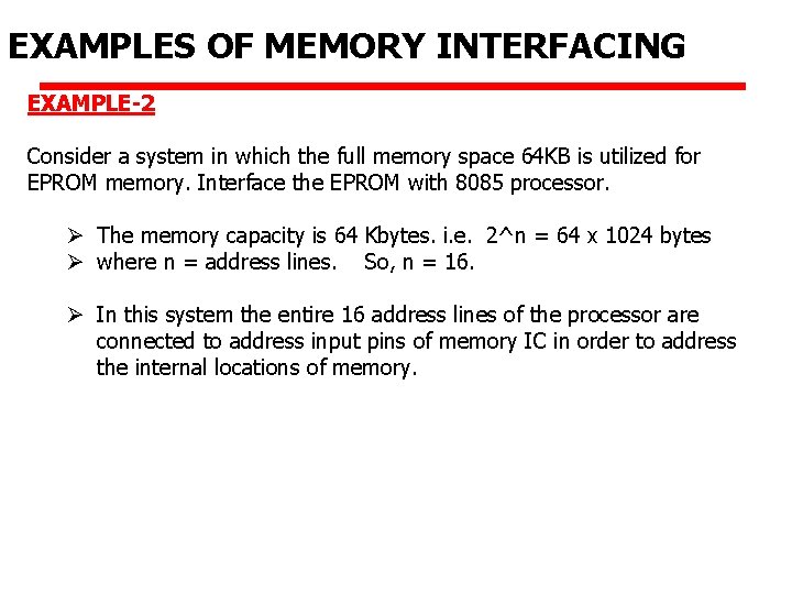
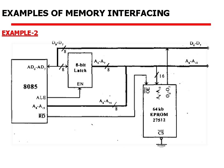
EXAMPLES OF MEMORY INTERFACING EXAMPLE-2 Consider a system in which the full memory space 64 KB is utilized for EPROM memory. Interface the EPROM with 8085 processor. Ø The memory capacity is 64 Kbytes. i. e. 2^n = 64 x 1024 bytes Ø where n = address lines. So, n = 16. Ø In this system the entire 16 address lines of the processor are connected to address input pins of memory IC in order to address the internal locations of memory.

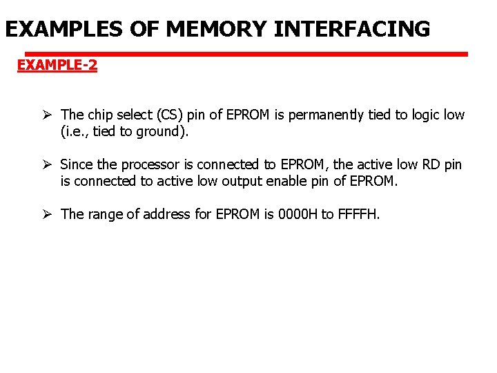
EXAMPLES OF MEMORY INTERFACING EXAMPLE-2 Ø The chip select (CS) pin of EPROM is permanently tied to logic low (i. e. , tied to ground). Ø Since the processor is connected to EPROM, the active low RD pin is connected to active low output enable pin of EPROM. Ø The range of address for EPROM is 0000 H to FFFFH.

EXAMPLES OF MEMORY INTERFACING EXAMPLE-2

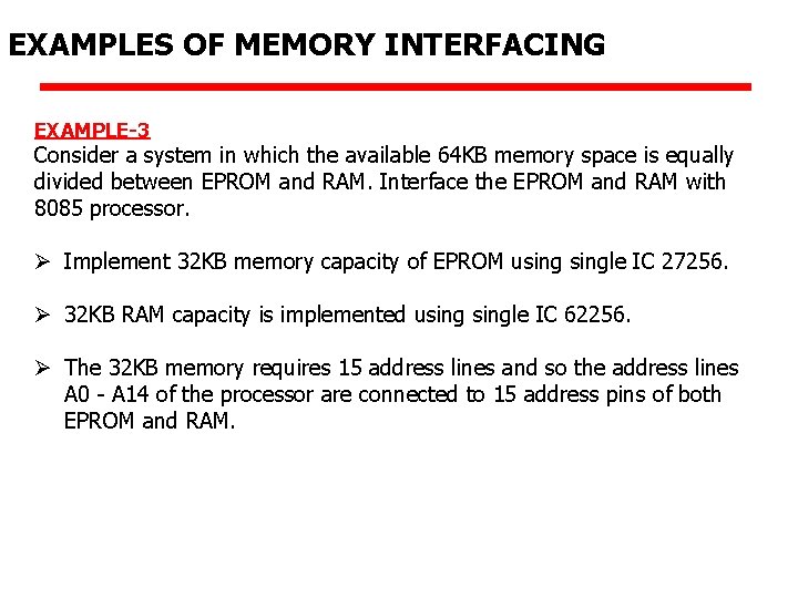
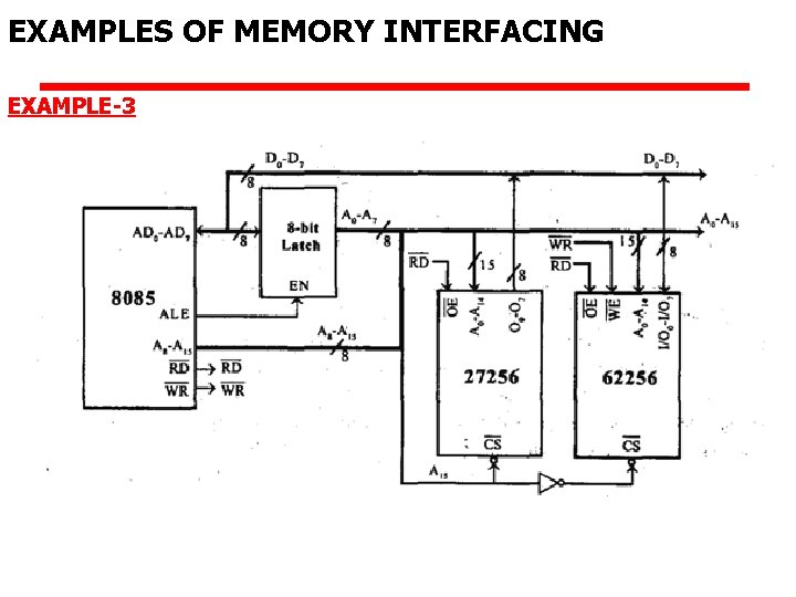
EXAMPLES OF MEMORY INTERFACING EXAMPLE-3 Consider a system in which the available 64 KB memory space is equally divided between EPROM and RAM. Interface the EPROM and RAM with 8085 processor. Ø Implement 32 KB memory capacity of EPROM usingle IC 27256. Ø 32 KB RAM capacity is implemented usingle IC 62256. Ø The 32 KB memory requires 15 address lines and so the address lines A 0 - A 14 of the processor are connected to 15 address pins of both EPROM and RAM.

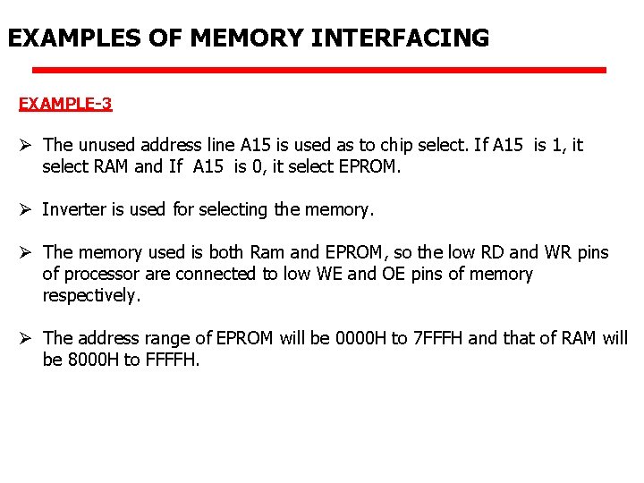
EXAMPLES OF MEMORY INTERFACING EXAMPLE-3 Ø The unused address line A 15 is used as to chip select. If A 15 is 1, it select RAM and If A 15 is 0, it select EPROM. Ø Inverter is used for selecting the memory. Ø The memory used is both Ram and EPROM, so the low RD and WR pins of processor are connected to low WE and OE pins of memory respectively. Ø The address range of EPROM will be 0000 H to 7 FFFH and that of RAM will be 8000 H to FFFFH.

EXAMPLES OF MEMORY INTERFACING EXAMPLE-3

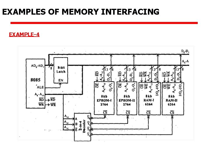
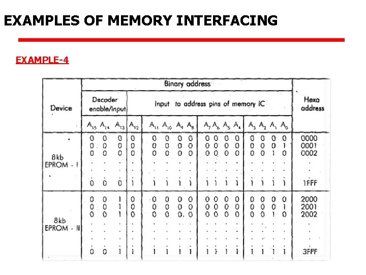
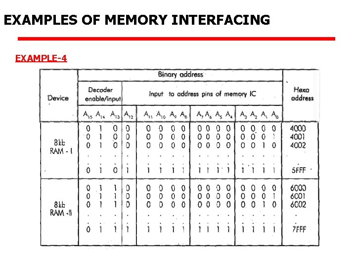
EXAMPLES OF MEMORY INTERFACING EXAMPLE-4 Consider a system in which 32 KB memory space is implemented using four numbers of 8 KB memory. Interface the EPROM and RAM with 8085 processor. Ø The total memory capacity is 32 KB. So, let two number of 8 KB memory be EPROM and the remaining two numbers be RAM. Ø Each 8 KB memory requires 13 address lines and so the address lines A 0 - A 12 of the processor are connected to 13 address pins of all the memory.

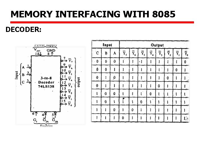
EXAMPLES OF MEMORY INTERFACING EXAMPLE-4 Ø The address lines and A 13 - A 14 can be decoded using a 2 -to-4 decoder to generate four chip select signals. Ø These four chip select signals can be used to select one of the four memory IC at any one time. Ø The address line A 15 is used as enable for decoder. Ø The simplified schematic memory organization is shown.

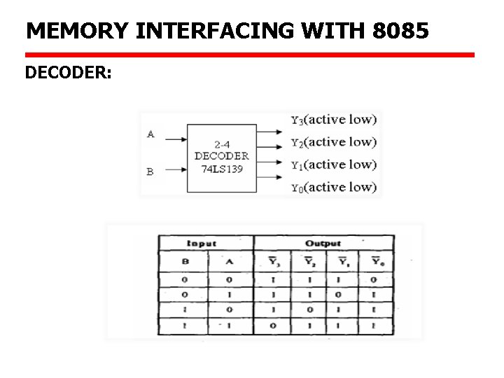
MEMORY INTERFACING WITH 8085 DECODER:

EXAMPLES OF MEMORY INTERFACING EXAMPLE-4

EXAMPLES OF MEMORY INTERFACING EXAMPLE-4

EXAMPLES OF MEMORY INTERFACING EXAMPLE-4

MEMORY INTERFACING WITH 8085 DECODER:

REVIEW