MICROPROCESSOR MODULE 3 INTEL 8086 8088 P IMPORTANT


 • Min mode • Pin 33 (MN/MX)")


 cycle = four clock cycles, • Each CLK")


 hold the address of")
 • Step 2 27")
 • Step 3 28")
 • Step 4 29")
 • Step 5 30")
 • Step 6 31")


- Slides: 40
MICROPROCESSOR MODULE 3 INTEL 8086 & 8088 µP IMPORTANT DETAILS 8086 16 BIT µP 8088 8 BIT µP
MAIN DIFFERENCE B/W 8088 & 8086 v 8086 16 BIT µP v 8088 8 BIT VERSION OF 8086 v INTERNALLY SAME ARCHITECTURE THEN WHY 8 BIT ? • BECAUSE IN 8080, 8085: I/O DEVICES 8 BIT DATA PATHS, SO CODING DIFFERNCE IN 16 BIT µP
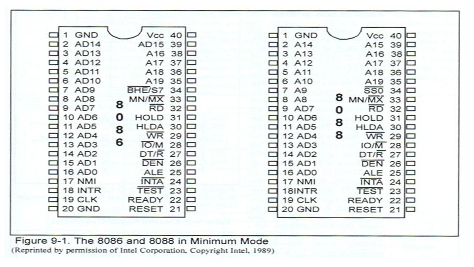
v NEXT SLIDE SHOWS THE PIN DIAGRAMS IN DIL PACKAGE FOR 8088 AND 8086 IN MINIMUM MODE
2 MODES OF OERATIONS IN 8086 & 8088 v MINIMUM MODE v MAXIMUM MODE v IN MODE, µP OPERATES AS SINGLE PROCESSOR IN THE COMPUTER v IN MAX MODE, µP OPERATES IN MULTIPROCESSOR SYSTEM. HOW? q BY INTERFACING EXTRA µP, Ics and USING: q STATUS SIGNALS: S 0, S 1. S 2
MAXIMUM MODE
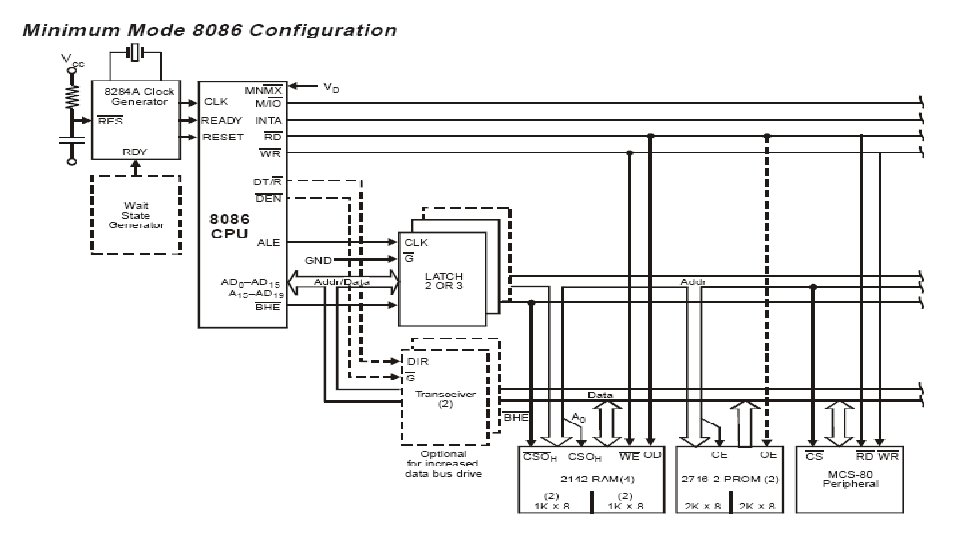
SEPARATION of DATA AND ADRS BUS IN 8086/8088 v AD 0 TO AD 15 ARE MUXED v MAY BE SEPARATED IN MANY WAYS v ONE WAY IS SHOWN IN NEXT SLIDE USING D LATCHES v ADRS BITS ARE LATCHED BEFORE THEY BECOME DATA BITS
DEMUXING OF ADRS & DATA BUSSES IN 8088
Min / Max Mode (Pin 24– 31) • Min mode • Pin 33 (MN/MX) to +5 V, Logic 1 • Pin 24 -31 are used as memory and I/O control signal • Control signals generated internally by the 8086/88 • More cost-effective • Max mode • Pin #33 (MN/MX) to GD • Some control signals generated by 8288 bus controller • Max mode is used when math 8087 MATH P is used Engr 4862 Microprocessors
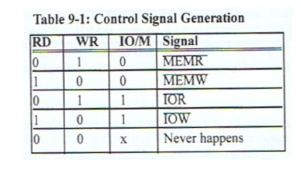
MAX MODE STATUS PINS: S 0, S 1, S 2, S 1, S 0 0 0 1 1 1 0 0 1 1 1 connect directly to 8288 INTA Interrupt Acknowledgment IORC Read I/O Port IOWC Write I/O Port NONE Halt MRDC Code Access MRDC Read Memory MWTC Write Memory Passive None
Clock in µP • Clock signal is important to operation of a µP ct. • Synchronizes sequential activities of µP and computer system Engr 4862 Microprocessors
µP clock Rate • The speed at which µP executes instructions. EVERY P contains an internal clock that regulates the rate at which instructions are executed and synchronizes all the various computer components. • µP requires a number of clock cycles to execute each instruction. Faster the clock, more instructions the P can execute per second. Clock speeds are in MHz or GHz • Some µP are superscalar, which means they can execute more than one instruction per clock cycle • Like Ps, expansion buses also have clock speeds. Ideally, P clock speed and bus clock speed should be t same so that neither component slows down the other. In practice, bus clock speed is slower than P clock speed, which creates a bottleneck 12
8284 Clock Generator & Driver IC 33% Duty Cycle
8284 PIN DIAGRAM Engr 4862 Microprocessors
Why 8284 Clock Generator • Provides proper clock signal • Uses a crystal oscillator (3 oscillations per clock) • Provides correct waveforms for other signals to µP For: • RESET • Request for wait state Engr 4862 Microprocessors
8284 DETAILS • 18 -pin chip. Provides clock • synchronization for µP • READY signal for insertion of WAIT states into µP bus cycle • Input Pins • RES (Reset In): from power supply • X 1 and X 2 (Crystal In): crystal f must be 3 times desired f for µP • For IBM PC, 14. 31818 MHz (max 24 MHz) • RDY 1 and AEN 1: provide a Ready signal to m. Pro, which will insert a WAIT state to µP read/write cycle. • RDY 2 and AEN 2: For multiprocessor systems Engr 4862 Microprocessors
8284 DETAILS • Output Signals • RESET: To reset 8086/88, activated by RES • OSC (oscillator): provide to the expansion slot • CLK (clock): 1/3 of the OSC or EFI input, with a duty cycle of 33% • In IBM PC, OSC = 14. 31818 MHz, so CLK = 4. 772776 MHz • PCLK: one-half of CLK (1/6 of crystal) with duty cycle of 50% and is TTL compatible. Provide to 8253 Timer to generate speaker tones • READY: connect to READY input of µP to insert WAIT state Engr 4862 Microprocessors
TIMING: Machine Cycles AKA Bus Cycles • Def • • One discrete information transfer on the buses • This includes the address, data, and control information Engr 4862 Microprocessors
Timing • Period of one bus cycle is at least 4 times a clock cycle • In 10 -MHz 8086 µP • Each clock cycle has a period of 100 ns • Machine cycle period is 400 n. S Engr 4862 Microprocessors
Timing 400 ns 100 ns Engr 4862 Microprocessors 20
Machine Cycles • If machine (bus) cycle = four clock cycles, • Each CLK cycle called a T state • A defined action occurs during T 1, T 2, T 3, T 4 states: • T 1: Address is output • T 2: Bus cycle type (Mem/IO, read/write) • T 3: Data is supplied • T 4: Data latched by µP, then control signals removed Engr 4862 Microprocessors
Timing Wait state inserted here Engr 4862 Microprocessors
• Why T states? • In 8086/8088, address and data lines are multiplexed • µP needs time to change signals during each bus cycle • Memory devices need time to decipher address value and then read/write the data (access time) Engr 4862 Microprocessors
Timing • system clock has a constant period, bus cycle does not • Slow devices (memory or I/O) may need extra time • µP inserts extra wait states b/w states T 3 and T 4 • Alternatives are: • to slow down system clock • or to use faster devices Engr 4862 Microprocessors
Fetching & Execution Cycles • Fetching Cycle • Takes the instruction required from MM, stores it in instruction register, and moves the program counter Reg (P C)/ Insturction Pointer Reg (IP) , on one, so that it points to next instruction. • Execute cycle • Actual actions occur during execute cycle of instruction. • Depend on both type of instruction and addressing mode specified to access required data 25
Fetching an instruction • Step 1 Instruction pointer (program counter) hold the address of the next instruction to be fetch. 26
FETCHING AN INSTRUCTION (cont. ) • Step 2 27
FETCHING AN INSTRUCTION (cont. ) • Step 3 28
FETCHING AN INSTRUCTION (cont. ) • Step 4 29
FETCHING AN INSTRUCTION (cont. ) • Step 5 30
FETCHING AN INSTRUCTION (cont. ) • Step 6 31
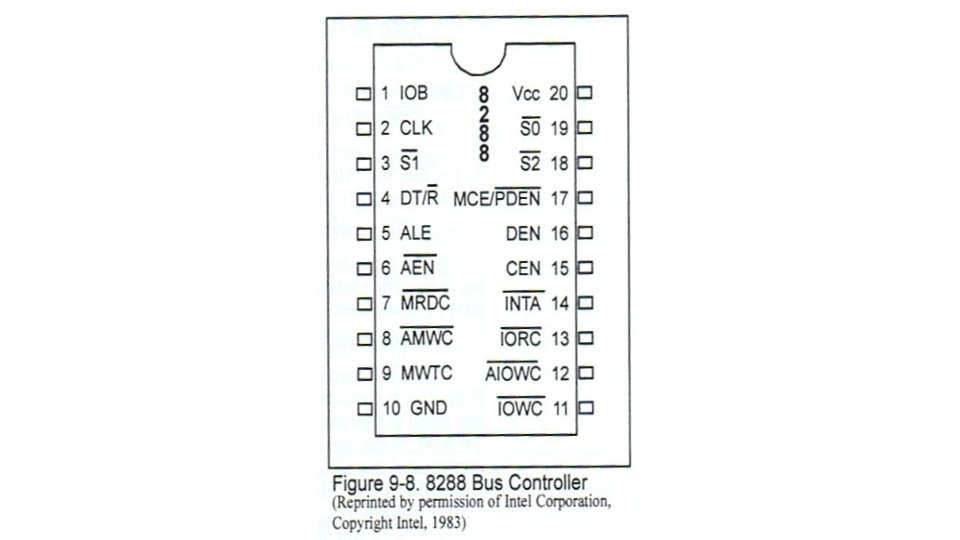
Other Supporting Chips • 8288 Bus Controller • A 20 -pin chip to provide all control signals when the 8086/88 is in the maximum mode • 74 LS 373 Latch • Provide isolation and bus boosting • 74 LS 244 Unidirectional data transceiver chip • 74 LS 245 Bidirectional data transceiver chip • Provide bus buffering and boosting Engr 4862 Microprocessors
8288 Bus Controller Engr 4862 Microprocessors
Programmable Peripheral I/O 8255 PPI : 40 -pin DIP IC provides 3 programmable I/O ports, A, B, and C. v Each port may be programmed as to be input or output port, flexible than (74 LS 373, 73 LS 244, Ics which must be hardwired) v Engr 4862 Microprocessors
8255 Design Example A 2 System Address Bus D 0 D 7 IOW IOR WR RD A 0 A 1 CS A 7 Engr 4862 Microprocessors A B CL CH
8255 Design Example • Any of ports A, B, C can be programmed as input or output • Port can not be both an input and output port at the same time • Port C can be programmed with CL, CH separately Engr 4862 Microprocessors
COMPARISON MIN MODE ONE 8086 ONLY ALE BY 8086 INTA BY 8086 CT SIMPLE LOW PERFORMANCE MAX MODE MAY BE MULYIPLE Ps ALE BY BUS CONTROLLER 8288 IC INTA BY 8288 CT COMLEX HIGH PERFORMANCE