Microprocessor Design in the Face of Process Variations









- Slides: 52

Microprocessor Design in the Face of Process Variations Csaba Andras Moritz Electrical & Computer Engineering University of Massachusetts, Amherst Nov, 2007 Csaba Andras Moritz © 2007

Outline l Introduction l Impact of Process Variations l A Process Variation Resilient Pipeline l A Process Variation Resilient Adaptive Cache Architecture l Results l Conclusion Csaba Andras Moritz - Software Systems & Architecture Lab, Electrical & Computer Engineering; © 2007

Introduction l As technology scales, the feature size reduces thereby requiring a sophisticated fabrication process. l The process variations increase as the feature reduces due to the difficulty of fabricating small structures consistently across a die or a wafer. l These variations cause mismatches between identical structures. Device and interconnect variation trends l With respect to circuits, this translates to a change in all devices or interconnects parameters from their mean value. for different technology generations Sani Nassif, etl. “Models of Process Variations in Device and Interconnect”. IEEE Press 2000 Csaba Andras Moritz - Software Systems & Architecture Lab, Electrical & Computer Engineering; © 2007

Introduction l Two main sources of process variation: ¨ ¨ l Physical factors (intrinsic variation) Environmental factors (dynamic variation) The physical factors are permanent and result from limitations in the fabrication process ¨ Effective Channel Length (Geometric Variations): l ¨ Threshold Voltage (Electrical Parameter Variation): l l Variation in device geometry Random dopant fluctuations changes in oxide thickness The environmental factors depend on the operation of the circuit and include variations in: ¨ l Imperfections in photolithography (mask, lens, photo system deviations) Temperature, Power Supply, Switching Activity The performance and power consumption of integrated circuits can be greatly affected. Csaba Andras Moritz - Software Systems & Architecture Lab, Electrical & Computer Engineering; © 2007

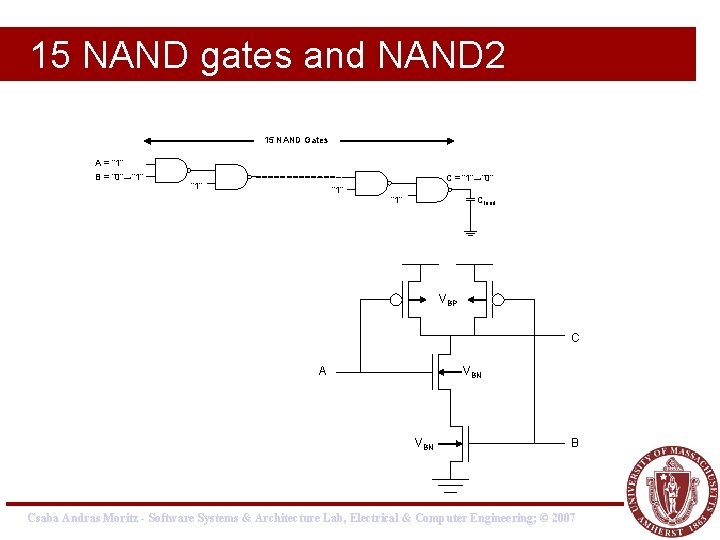
Pipeline design l 10 -20 gate delays typically l Let us review variation with a NAND chain Csaba Andras Moritz - Software Systems & Architecture Lab, Electrical & Computer Engineering; © 2007

15 NAND gates and NAND 2 15 NAND Gates A = “ 1” B = “ 0”→“ 1” C = “ 1”→“ 0” “ 1” Cload VBP C A VBN B Csaba Andras Moritz - Software Systems & Architecture Lab, Electrical & Computer Engineering; © 2007

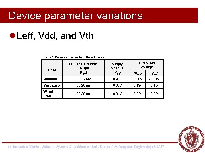
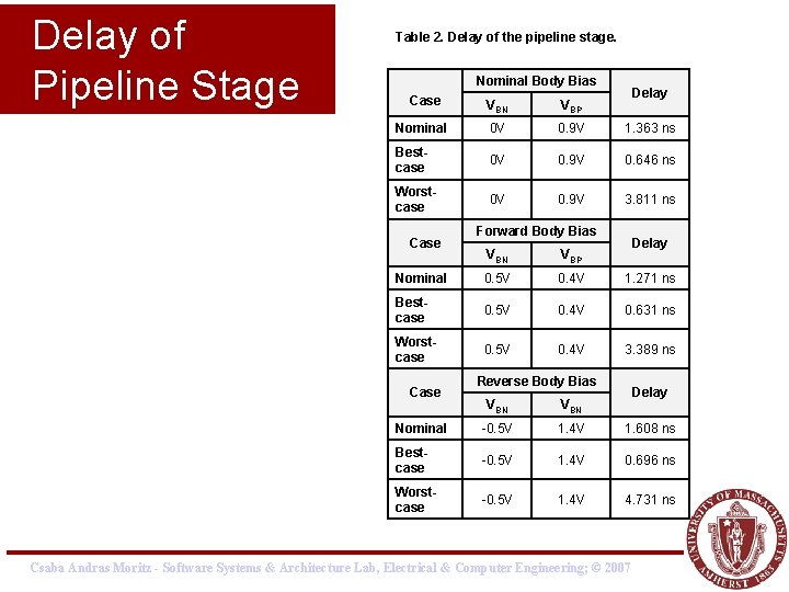
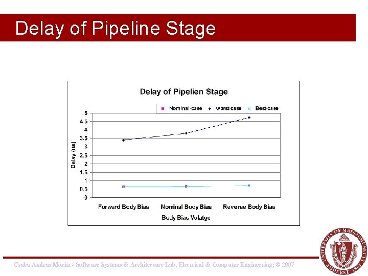
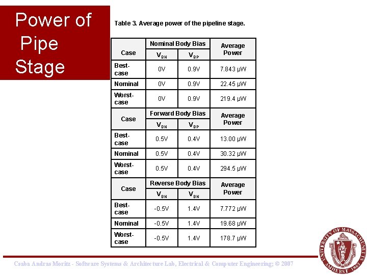
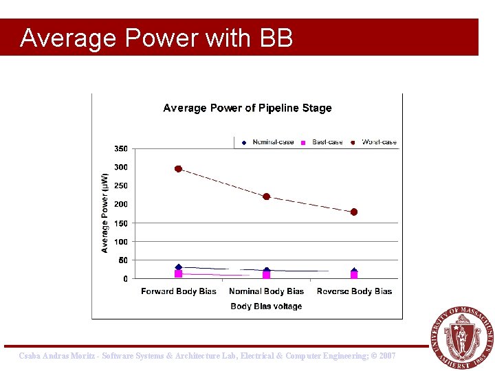
Assumptions l We target a future 32 -nm technology process where leakage and process variation are significant l In the nominal delay we assume there is no process variations impact on the pipeline stage. l In worst-case we assume the worst values of the parameter variations at each transistor that will result in the maximum delay or power consumption. l A body bias is a voltage applied between the source or drain of a transistor and its substrate, effectively changing the transistor’s Vth. l Depending on the polarity of the voltage applied, Vth increases or decreases. If it increases, the transistor becomes less leaky and slower (reverse body bias); if it decreases, the transistor becomes leakier and faster (forward body bias). l Table 1 shows parameter values of process variations for different cases. Figure 3 and Table 2 show delay of the pipeline at different body bias voltages. Figure 4 and Table 3 show average power consumption of the pipeline stage with different body bias voltages. Csaba Andras Moritz - Software Systems & Architecture Lab, Electrical & Computer Engineering; © 2007

Device parameter variations l Leff, Vdd, and Vth Table 1. Parameter values for different cases Threshold Voltage Effective Channel Length (Leff) Supply Voltage (Vdd) (Vthn) (Vthp) Nominal 25. 32 nm 0. 90 V 0. 20 V -0. 21 V Best-case 20. 26 nm 0. 96 V 0. 18 V -0. 19 V Worstcase 30. 38 nm 0. 84 V 0. 22 V -0. 23 V Case Csaba Andras Moritz - Software Systems & Architecture Lab, Electrical & Computer Engineering; © 2007

Delay of Pipeline Stage Table 2. Delay of the pipeline stage. Nominal Body Bias Delay Case VBN VBP Nominal 0 V 0. 9 V 1. 363 ns Bestcase 0 V 0. 9 V 0. 646 ns Worstcase 0 V 0. 9 V 3. 811 ns Case Forward Body Bias Delay VBN VBP Nominal 0. 5 V 0. 4 V 1. 271 ns Bestcase 0. 5 V 0. 4 V 0. 631 ns Worstcase 0. 5 V 0. 4 V 3. 389 ns Case Reverse Body Bias Delay VBN Nominal -0. 5 V 1. 4 V 1. 608 ns Bestcase -0. 5 V 1. 4 V 0. 696 ns Worstcase -0. 5 V 1. 4 V 4. 731 ns Csaba Andras Moritz - Software Systems & Architecture Lab, Electrical & Computer Engineering; © 2007

Delay of Pipeline Stage Csaba Andras Moritz - Software Systems & Architecture Lab, Electrical & Computer Engineering; © 2007

Power of Pipe Stage Table 3. Average power of the pipeline stage. Nominal Body Bias Case Average Power VBN VBP Bestcase 0 V 0. 9 V 7. 843 μW Nominal 0 V 0. 9 V 22. 45 μW Worstcase 0 V 0. 9 V 219. 4 μW Case Forward Body Bias Average Power VBN VBP Bestcase 0. 5 V 0. 4 V 13. 00 μW Nominal 0. 5 V 0. 4 V 30. 32 μW Worstcase 0. 5 V 0. 4 V 294. 5 μW Case Reverse Body Bias Average Power VBN Bestcase -0. 5 V 1. 4 V 7. 772 μW Nominal -0. 5 V 1. 4 V 19. 68 μW Worstcase -0. 5 V 1. 4 V 178. 7 μW Csaba Andras Moritz - Software Systems & Architecture Lab, Electrical & Computer Engineering; © 2007

Average Power with BB Csaba Andras Moritz - Software Systems & Architecture Lab, Electrical & Computer Engineering; © 2007

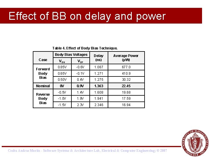
Effect of BB on delay and power Table 4. Effect of Body Bias Technique. Body Bias Voltages Case Forward Body Bias Nominal Reverse Body Bias Delay (ns) Average Power (μW) VBN VBP 0. 85 V -0. 6 V 1. 087 677. 0 0. 65 V -0. 1 V 1. 271 410. 9 0. 50 V 0. 4 V 1. 275 30. 32 0 V 0. 9 V 1. 363 22. 45 -0. 5 V 1. 4 V 1. 608 19. 68 -1. 0 V 1. 941 17. 59 -1. 5 V 2. 346 16. 94 Csaba Andras Moritz - Software Systems & Architecture Lab, Electrical & Computer Engineering; © 2007

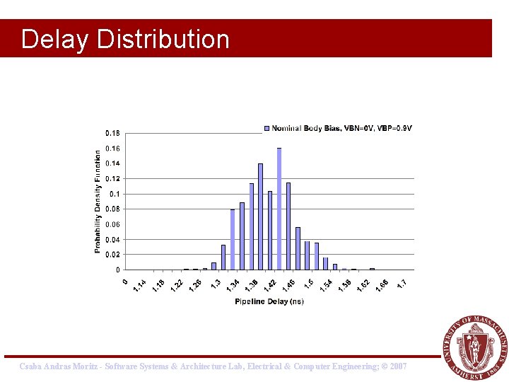
Delay Distribution Csaba Andras Moritz - Software Systems & Architecture Lab, Electrical & Computer Engineering; © 2007

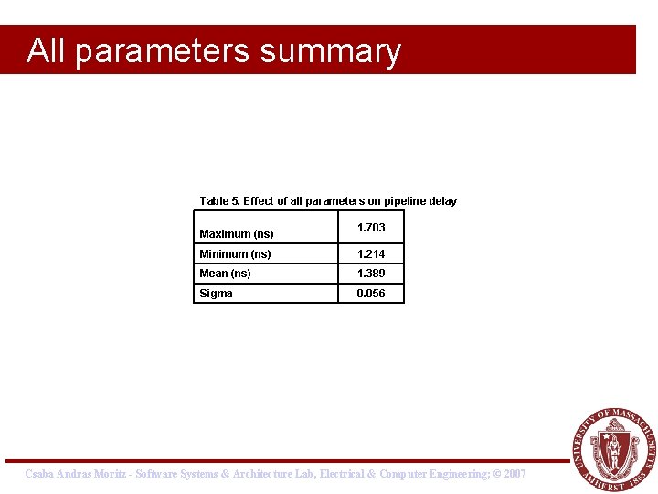
All parameters summary Table 5. Effect of all parameters on pipeline delay Maximum (ns) 1. 703 Minimum (ns) 1. 214 Mean (ns) 1. 389 Sigma 0. 056 Csaba Andras Moritz - Software Systems & Architecture Lab, Electrical & Computer Engineering; © 2007

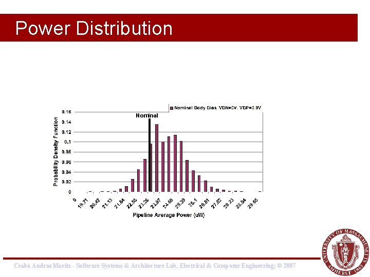
Power Distribution Nominal Csaba Andras Moritz - Software Systems & Architecture Lab, Electrical & Computer Engineering; © 2007

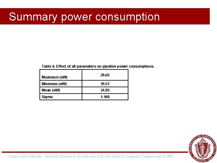
Summary power consumption Table 6. Effect of all parameters on pipeline power consumptions. Maximum (u. W) 29. 65 Minimum (u. W) 19. 51 Mean (u. W) 24. 05 Sigma 1. 168 Csaba Andras Moritz - Software Systems & Architecture Lab, Electrical & Computer Engineering; © 2007

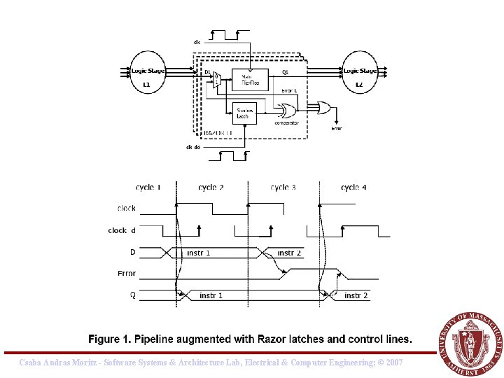
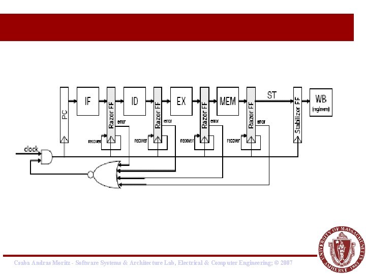
Razor Latches l Latch concept to sample output of a stage two different times l Compare outputs l If not equal resample inter-stage latch and delay pipeline by one cycle l Implications? Csaba Andras Moritz - Software Systems & Architecture Lab, Electrical & Computer Engineering; © 2007

Csaba Andras Moritz - Software Systems & Architecture Lab, Electrical & Computer Engineering; © 2007

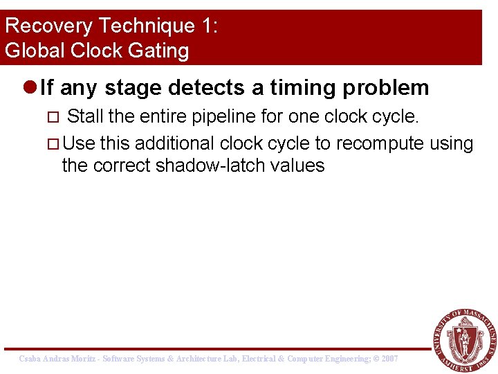
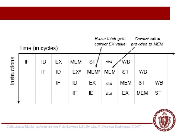
Recovery Technique 1: Global Clock Gating l If any stage detects a timing problem Stall the entire pipeline for one clock cycle. ¨ Use this additional clock cycle to recompute using the correct shadow-latch values ¨ Csaba Andras Moritz - Software Systems & Architecture Lab, Electrical & Computer Engineering; © 2007

Csaba Andras Moritz - Software Systems & Architecture Lab, Electrical & Computer Engineering; © 2007

Csaba Andras Moritz - Software Systems & Architecture Lab, Electrical & Computer Engineering; © 2007

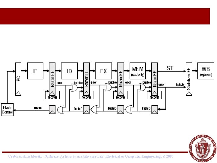
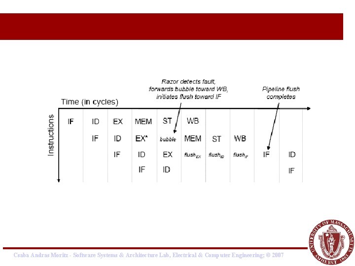
Recovery Technique 2: Counterflow Pipelining l When a mismatch (between regular and shadow latch contents) is detected: ¨ Assert a bubble signal, to specify that the erring pipeline slot is now to be considered a bubble. ¨ In the subsequent cycle, inject the shadow latch value into the next stage, allowing the errant operation to continue with the correct values ¨ Trigger a flush train, traveling backwards from the errant stage, flushing operations at each stage it visits Csaba Andras Moritz - Software Systems & Architecture Lab, Electrical & Computer Engineering; © 2007

Csaba Andras Moritz - Software Systems & Architecture Lab, Electrical & Computer Engineering; © 2007

Csaba Andras Moritz - Software Systems & Architecture Lab, Electrical & Computer Engineering; © 2007

Process Variation Impact on Memory Systems l The process variations are random in nature and are expected to become significant in the smaller geometry transistors commonly used in memories. l Process variations in caches affect the performance of circuits like ¨ ¨ ¨ l Sense amplifiers that require identical device characteristics SRAM cells that require near-minimum-sized cell stability for large arrays in embedded, low-power applications The delay of the address decoders suffer from the process variations that can result in shorter time left for accessing the SRAM cells Question is whethere is a significant delay variation overall that will drive a change in memory architecture design. Csaba Andras Moritz - Software Systems & Architecture Lab, Electrical & Computer Engineering; © 2007

Motivation l To account for the worst-case scenario we might need to increase the cache access time by 2 to 3 cycles in conventional design. l Application performance could be impacted by as much as 30 -40%! l These results suggest that process variations must be taken into consideration ¨ New types of circuits and architectures? Csaba Andras Moritz - Software Systems & Architecture Lab, Electrical & Computer Engineering; © 2007

Introduction l There are several ideas that could be exploited in a memory system: ¨ reduce performance by operating at a lower clock frequency (conservative approach) ¨ increase cache access latency assuming worst-case delay (conservative approach) ¨ variable-delay cache architecture (adaptive approach) Csaba Andras Moritz - Software Systems & Architecture Lab, Electrical & Computer Engineering; © 2007

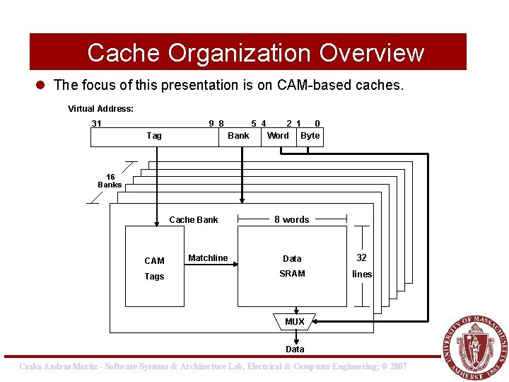
Cache Organization Overview l The focus of this presentation is on CAM-based caches. Virtual Address: 31 9 8 Tag 5 4 Bank 2 1 0 Word Byte 16 Banks Cache Bank CAM Tags Matchline 8 words Data 32 SRAM lines MUX Data Csaba Andras Moritz - Software Systems & Architecture Lab, Electrical & Computer Engineering; © 2007

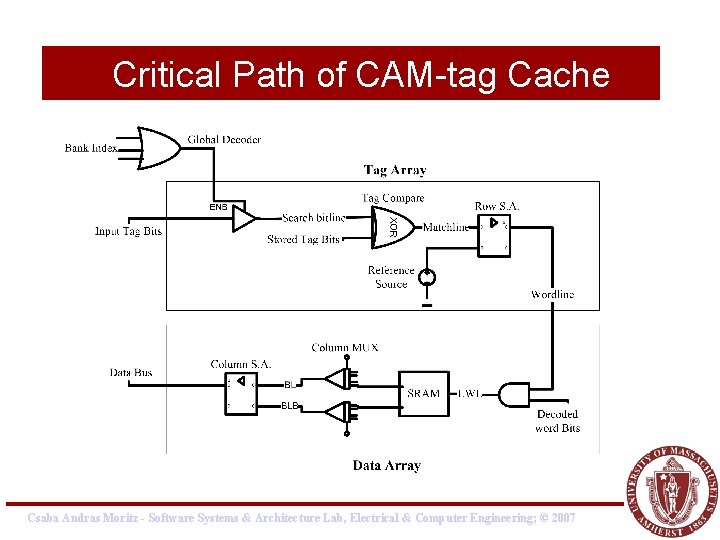
Critical Path of CAM-tag Cache Csaba Andras Moritz - Software Systems & Architecture Lab, Electrical & Computer Engineering; © 2007

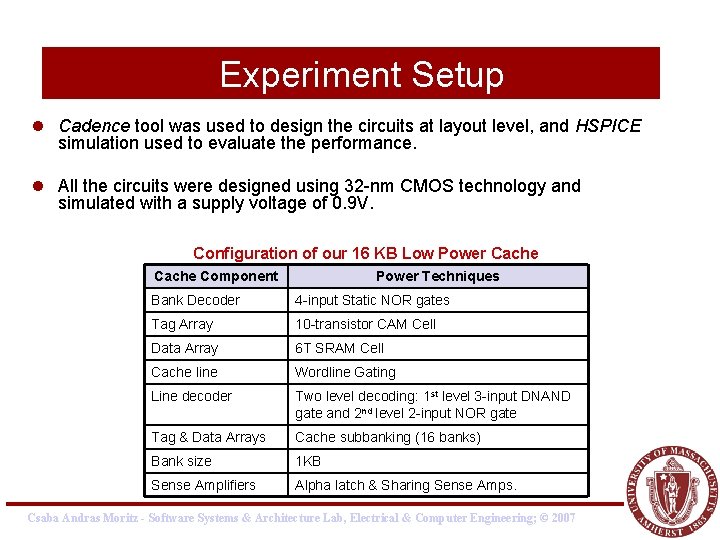
Experiment Setup l Cadence tool was used to design the circuits at layout level, and HSPICE simulation used to evaluate the performance. l All the circuits were designed using 32 -nm CMOS technology and simulated with a supply voltage of 0. 9 V. Configuration of our 16 KB Low Power Cache Component Power Techniques Bank Decoder 4 -input Static NOR gates Tag Array 10 -transistor CAM Cell Data Array 6 T SRAM Cell Cache line Wordline Gating Line decoder Two level decoding: 1 st level 3 -input DNAND gate and 2 nd level 2 -input NOR gate Tag & Data Arrays Cache subbanking (16 banks) Bank size 1 KB Sense Amplifiers Alpha latch & Sharing Sense Amps. Csaba Andras Moritz - Software Systems & Architecture Lab, Electrical & Computer Engineering; © 2007

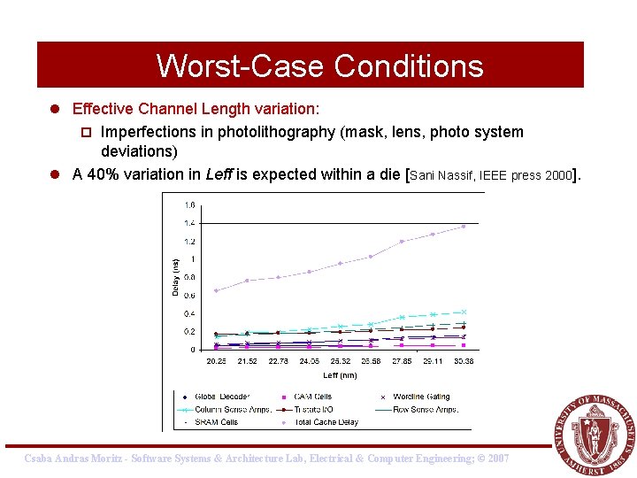
Worst-Case Conditions l Effective Channel Length variation: ¨ Imperfections in photolithography (mask, lens, photo system deviations) l A 40% variation in Leff is expected within a die [Sani Nassif, IEEE press 2000]. Csaba Andras Moritz - Software Systems & Architecture Lab, Electrical & Computer Engineering; © 2007

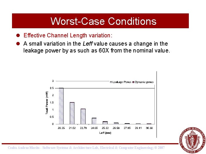
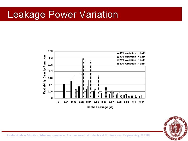
Worst-Case Conditions l Effective Channel Length variation: l A small variation in the Leff value causes a change in the leakage power by as such as 60 X from the nominal value. Csaba Andras Moritz - Software Systems & Architecture Lab, Electrical & Computer Engineering; © 2007

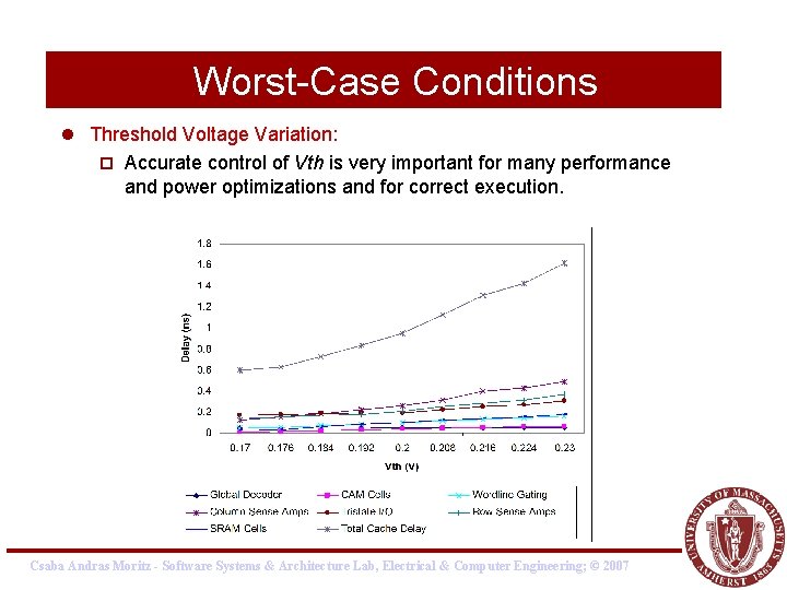
Worst-Case Conditions l Threshold Voltage Variation: ¨ Accurate control of Vth is very important for many performance and power optimizations and for correct execution. Csaba Andras Moritz - Software Systems & Architecture Lab, Electrical & Computer Engineering; © 2007

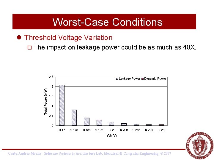
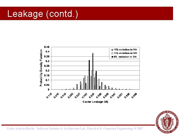
Worst-Case Conditions l Threshold Voltage Variation ¨ The impact on leakage power could be as much as 40 X. Csaba Andras Moritz - Software Systems & Architecture Lab, Electrical & Computer Engineering; © 2007

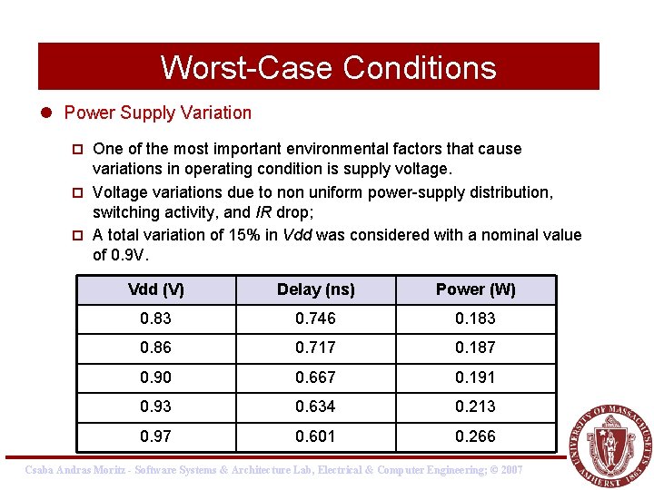
Worst-Case Conditions l Power Supply Variation One of the most important environmental factors that cause variations in operating condition is supply voltage. ¨ Voltage variations due to non uniform power-supply distribution, switching activity, and IR drop; ¨ A total variation of 15% in Vdd was considered with a nominal value of 0. 9 V. ¨ Vdd (V) Delay (ns) Power (W) 0. 83 0. 746 0. 183 0. 86 0. 717 0. 187 0. 90 0. 667 0. 191 0. 93 0. 634 0. 213 0. 97 0. 601 0. 266 Csaba Andras Moritz - Software Systems & Architecture Lab, Electrical & Computer Engineering; © 2007

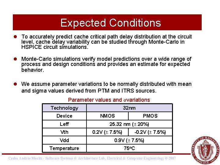
Expected Conditions l To accurately predict cache critical path delay distribution at the circuit level, cache delay variability can be studied through Monte-Carlo in HSPICE circuit simulations. l Monte-Carlo simulations verify model predictions over a wide range of process and design conditions and provides an estimate for expected behavior. l We assume parameter variations to be normally distributed with mean and sigma values derived from PTM and ITRS sources. Parameter values and σvariations Technology Device Leff Vth 32 nm NMOS PMOS 25. 32 nm (± 20%) 0. 2 V (± 7. 5%) -0. 2 V (± 7. 5%) Vdd 0. 9 V (± 7. 5%) Temperature 75 o. C Csaba Andras Moritz - Software Systems & Architecture Lab, Electrical & Computer Engineering; © 2007

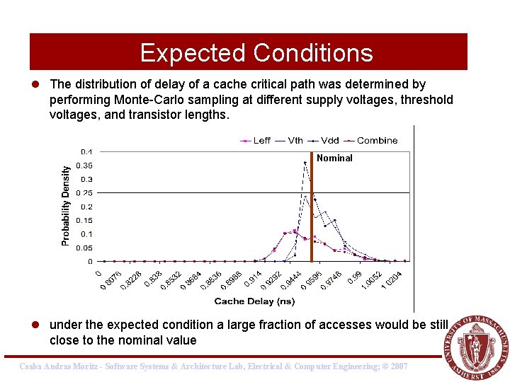
Expected Conditions l The distribution of delay of a cache critical path was determined by performing Monte-Carlo sampling at different supply voltages, threshold voltages, and transistor lengths. Nominal l under the expected condition a large fraction of accesses would be still close to the nominal value Csaba Andras Moritz - Software Systems & Architecture Lab, Electrical & Computer Engineering; © 2007

Architectural Techniques l How do we design a memory system in the face of process variations and help mitigate the negative impact on performance? l We can select a cache design using worst case assumptions ¨ ALL VARIATIONS and ALL COMPONENTS on the critical path l Alternatively, we need to design circuits and architectures that would work adaptively depending on actual delay ¨ Process variation resilient design ¨ Resilience against delays in different parts of the cache Csaba Andras Moritz - Software Systems & Architecture Lab, Electrical & Computer Engineering; © 2007

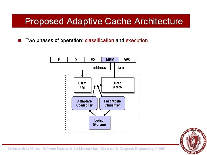
Proposed Adaptive Cache Architecture l Two phases of operation: classification and execution F D EX MEM address CAM Tag Adaptive Controller WB data Data Array Test Mode Classifier Delay Storage Csaba Andras Moritz - Software Systems & Architecture Lab, Electrical & Computer Engineering; © 2007

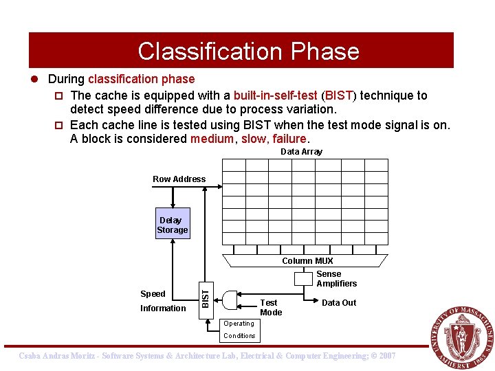
Classification Phase l During classification phase ¨ The cache is equipped with a built-in-self-test (BIST) technique to detect speed difference due to process variation. ¨ Each cache line is tested using BIST when the test mode signal is on. A block is considered medium, slow, failure. Data Array Row Address Delay Storage Column MUX Speed Information BIST Sense Amplifiers Test Mode Data Out Operating Conditions Csaba Andras Moritz - Software Systems & Architecture Lab, Electrical & Computer Engineering; © 2007

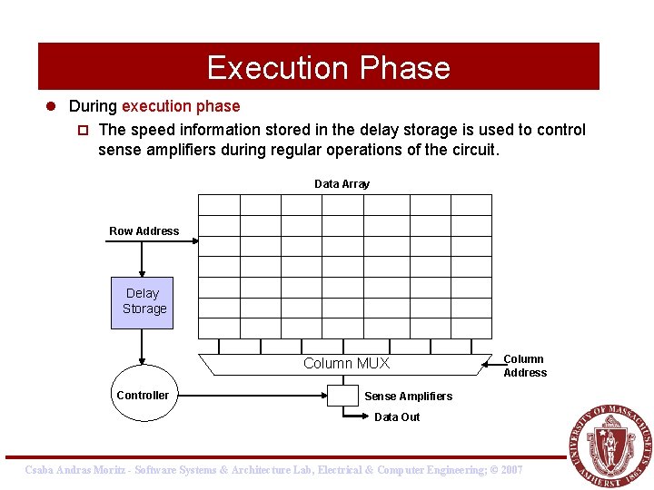
Execution Phase l During execution phase ¨ The speed information stored in the delay storage is used to control sense amplifiers during regular operations of the circuit. Data Array Row Address Delay Storage Column MUX Controller Column Address Sense Amplifiers Data Out Csaba Andras Moritz - Software Systems & Architecture Lab, Electrical & Computer Engineering; © 2007

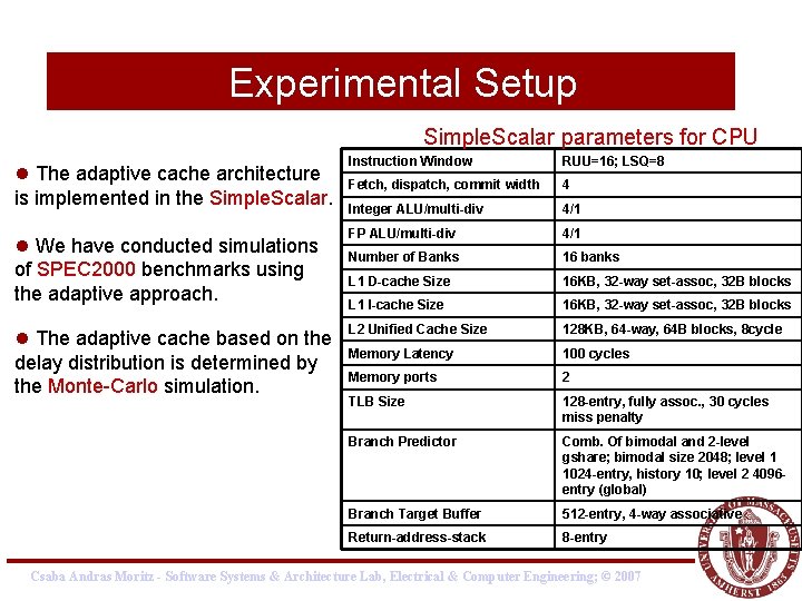
Experimental Setup Simple. Scalar parameters for CPU l The adaptive cache architecture is implemented in the Simple. Scalar. l We have conducted simulations of SPEC 2000 benchmarks using the adaptive approach. l The adaptive cache based on the delay distribution is determined by the Monte-Carlo simulation. Instruction Window RUU=16; LSQ=8 Fetch, dispatch, commit width 4 Integer ALU/multi-div 4/1 FP ALU/multi-div 4/1 Number of Banks 16 banks L 1 D-cache Size 16 KB, 32 -way set-assoc, 32 B blocks L 1 I-cache Size 16 KB, 32 -way set-assoc, 32 B blocks L 2 Unified Cache Size 128 KB, 64 -way, 64 B blocks, 8 cycle Memory Latency 100 cycles Memory ports 2 TLB Size 128 -entry, fully assoc. , 30 cycles miss penalty Branch Predictor Comb. Of bimodal and 2 -level gshare; bimodal size 2048; level 1 1024 -entry, history 10; level 2 4096 entry (global) Branch Target Buffer 512 -entry, 4 -way associative Return-address-stack 8 -entry Csaba Andras Moritz - Software Systems & Architecture Lab, Electrical & Computer Engineering; © 2007

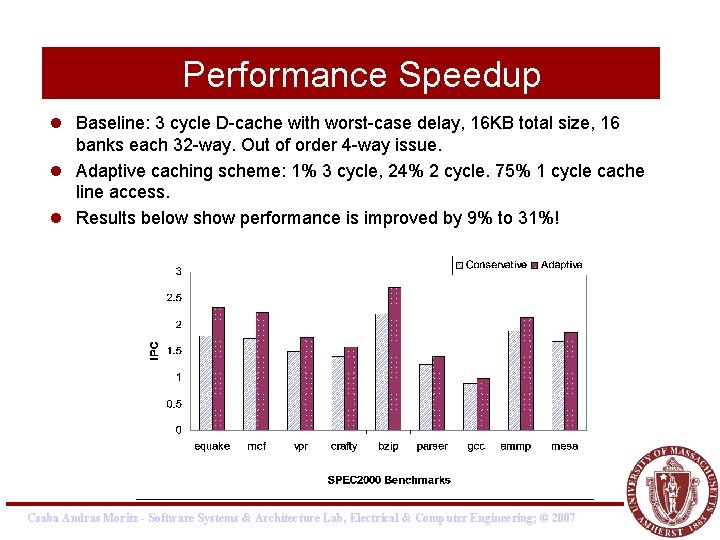
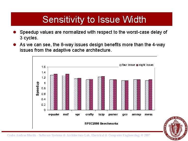
Performance Speedup l Baseline: 3 cycle D-cache with worst-case delay, 16 KB total size, 16 banks each 32 -way. Out of order 4 -way issue. l Adaptive caching scheme: 1% 3 cycle, 24% 2 cycle. 75% 1 cycle cache line access. l Results below show performance is improved by 9% to 31%! Csaba Andras Moritz - Software Systems & Architecture Lab, Electrical & Computer Engineering; © 2007

Sensitivity to Issue Width l Speedup values are normalized with respect to the worst-case delay of 3 cycles. l As we can see, the 8 -way issues design benefits more than the 4 -way issues from the adaptive cache architecture. Csaba Andras Moritz - Software Systems & Architecture Lab, Electrical & Computer Engineering; © 2007

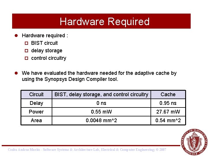
Hardware Required l Hardware required : ¨ BIST circuit ¨ delay storage ¨ control circuitry l We have evaluated the hardware needed for the adaptive cache by using the Synopsys Design Compiler tool. Circuit BIST, delay storage, and control circuitry Cache Delay 0 ns 0. 95 ns Power 0. 55 m. W 27. 67 m. W Area 0. 0048 mm^2 0. 54 mm^2 Csaba Andras Moritz - Software Systems & Architecture Lab, Electrical & Computer Engineering; © 2007

Power Issues Csaba Andras Moritz - Software Systems & Architecture Lab, Electrical & Computer Engineering; © 2007

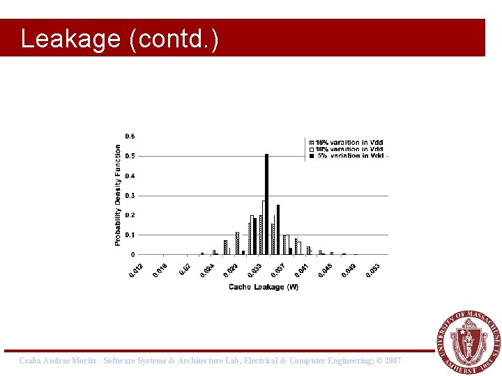
Leakage Power Variation Csaba Andras Moritz - Software Systems & Architecture Lab, Electrical & Computer Engineering; © 2007

Leakage (contd. ) Csaba Andras Moritz - Software Systems & Architecture Lab, Electrical & Computer Engineering; © 2007

Leakage (contd. ) Csaba Andras Moritz - Software Systems & Architecture Lab, Electrical & Computer Engineering; © 2007

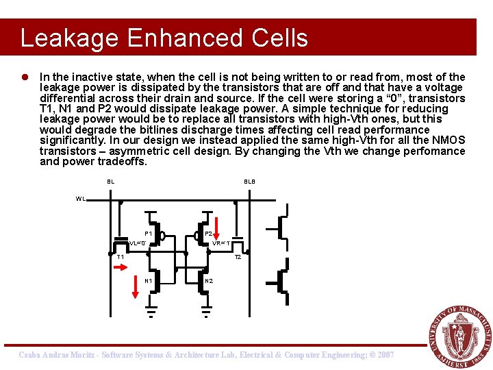
Leakage Enhanced Cells l In the inactive state, when the cell is not being written to or read from, most of the leakage power is dissipated by the transistors that are off and that have a voltage differential across their drain and source. If the cell were storing a “ 0”, transistors T 1, N 1 and P 2 would dissipate leakage power. A simple technique for reducing leakage power would be to replace all transistors with high-Vth ones, but this would degrade the bitlines discharge times affecting cell read performance significantly. In our design we instead applied the same high-Vth for all the NMOS transistors – asymmetric cell design. By changing the Vth we change perfomance and power tradeoffs. BL BLB WL P 1 VL=‘ 0’ P 2 VR=‘ 1’ T 1 T 2 N 1 N 2 Csaba Andras Moritz - Software Systems & Architecture Lab, Electrical & Computer Engineering; © 2007

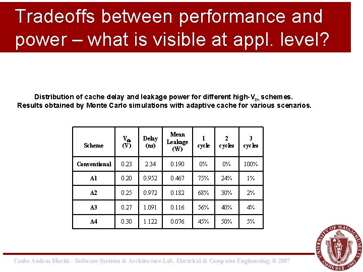
Tradeoffs between performance and power – what is visible at appl. level? Distribution of cache delay and leakage power for different high-Vth schemes. Results obtained by Monte Carlo simulations with adaptive cache for various scenarios. Scheme Vth (V) Delay (ns) Mean Leakage (W) 1 cycle 2 cycles 3 cycles Conventional 0. 23 2. 34 0. 190 0% 0% 100% A 1 0. 20 0. 952 0. 467 75% 24% 1% A 2 0. 25 0. 972 0. 182 68% 30% 2% A 3 0. 27 1. 091 0. 116 56% 40% 4% A 4 0. 30 1. 122 0. 076 45% 50% 5% Csaba Andras Moritz - Software Systems & Architecture Lab, Electrical & Computer Engineering; © 2007