MICROELETTRONICA Design methodologies Lection 8 Design methodologies general
- Slides: 24

MICROELETTRONICA Design methodologies Lection 8

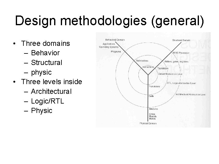
Design methodologies (general) • Three domains – Behavior – Structural – physic • Three levels inside – Architectural – Logic/RTL – Physic

Evaluation of an I. C: • • Performance – speed, power, function, flexibility Size of the die Time to design – i. e cost of engineering Easy of verification, test generation and testability BUT the system could be also realized by micro, FPGA, PAL, etc. ECONOMIC EVALUATION

Design principles • • Hierarchy Regularity Modularity Locality

Hierarchy • Divide and conquer • Divide in modules and repeating untill each submodule is comprehensible prebuilt component available • Virtual components IP

Regularity • Similar submodules • All level of design hierarchy: equal size transistors, standard cell type library, parameterized RAM, etc. • Design reuse

Modularity • Well defined functions and interfaces • Interaction with other modules well characterized • Behavioral, structural and physical interfaces (function, signals, electrical and timing constraints)

Locality • The internal variables of a module don’t interest other modules correspond to reduce global variables in HDL • Advantage for the clock

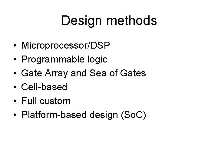
Design methods • • • Microprocessor/DSP Programmable logic Gate Array and Sea of Gates Cell-based Full custom Platform-based design (So. C)

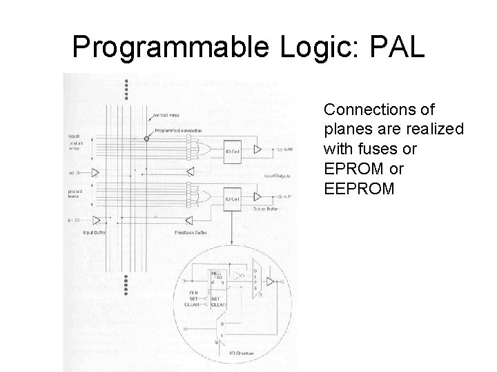
Programmable Logic: PAL Connections of planes are realized with fuses or EPROM or EEPROM

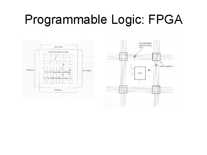
Programmable Logic: FPGA

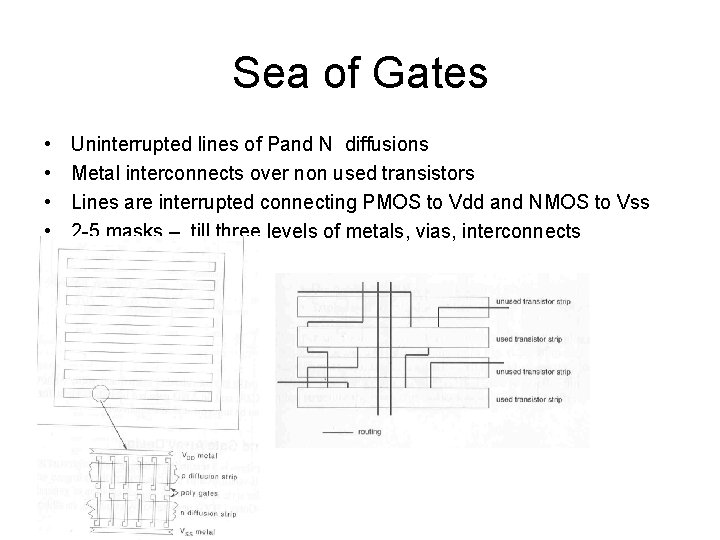
Sea of Gates • • Uninterrupted lines of Pand N diffusions Metal interconnects over non used transistors Lines are interrupted connecting PMOS to Vdd and NMOS to Vss 2 -5 masks – till three levels of metals, vias, interconnects

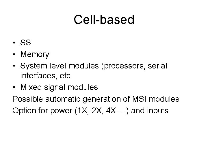
Cell-based • SSI • Memory • System level modules (processors, serial interfaces, etc. • Mixed signal modules Possible automatic generation of MSI modules Option for power (1 X, 2 X, 4 X…. ) and inputs

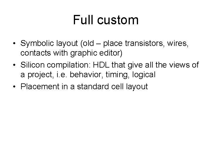
Full custom • Symbolic layout (old – place transistors, wires, contacts with graphic editor) • Silicon compilation: HDL that give all the views of a project, i. e. behavior, timing, logical • Placement in a standard cell layout

Platform-based design (So. C) • Processors, memory, I/O functions, FPGA • Use of IP, hw/sw codesign

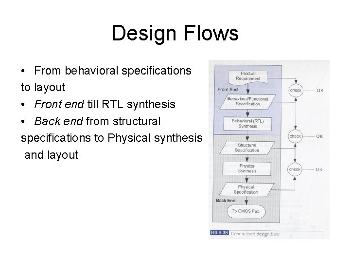
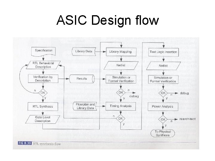
Design Flows • From behavioral specifications to layout • Front end till RTL synthesis • Back end from structural specifications to Physical synthesis and layout

ASIC Design flow Fig. 8. 39

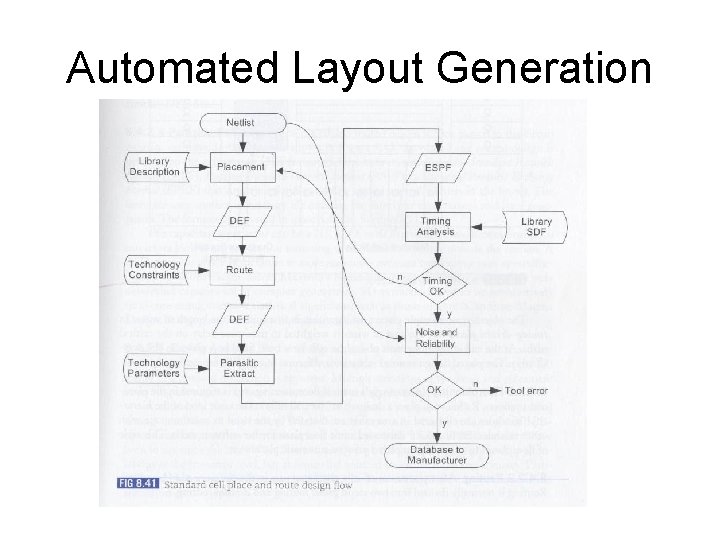
Automated Layout Generation Fig. 8. 41

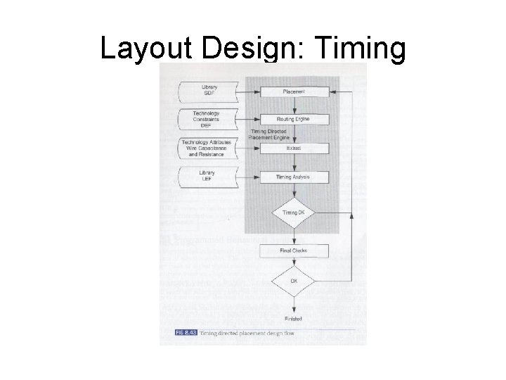
Layout Design: Timing Fig. 8. 43

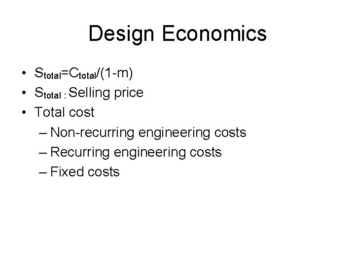
Design Economics • Stotal=Ctotal/(1 -m) • Stotal : Selling price • Total cost – Non-recurring engineering costs – Recurring engineering costs – Fixed costs

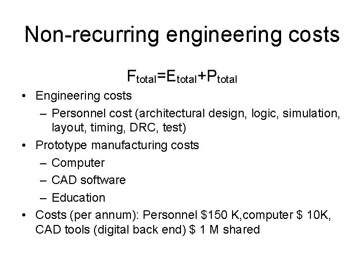
Non-recurring engineering costs Ftotal=Etotal+Ptotal • Engineering costs – Personnel cost (architectural design, logic, simulation, layout, timing, DRC, test) • Prototype manufacturing costs – Computer – CAD software – Education • Costs (per annum): Personnel $150 K, computer $ 10 K, CAD tools (digital back end) $ 1 M shared

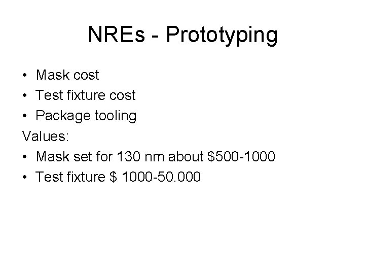
NREs - Prototyping • Mask cost • Test fixture cost • Package tooling Values: • Mask set for 130 nm about $500 -1000 • Test fixture $ 1000 -50. 000

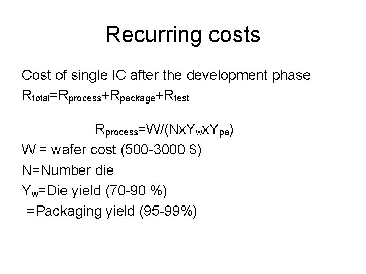
Recurring costs Cost of single IC after the development phase Rtotal=Rprocess+Rpackage+Rtest Rprocess=W/(Nx. Ywx. Ypa) W = wafer cost (500 -3000 $) N=Number die Yw=Die yield (70 -90 %) =Packaging yield (95 -99%)

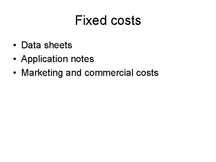
Fixed costs • Data sheets • Application notes • Marketing and commercial costs