Microelectronics Device Fabrication Vacuum Tube Devices Thermionic valve
Microelectronics & Device Fabrication
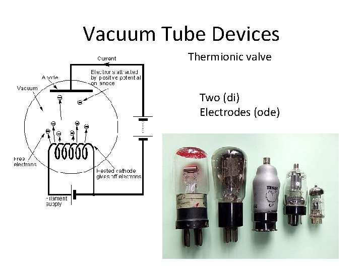
Vacuum Tube Devices Thermionic valve Two (di) Electrodes (ode)
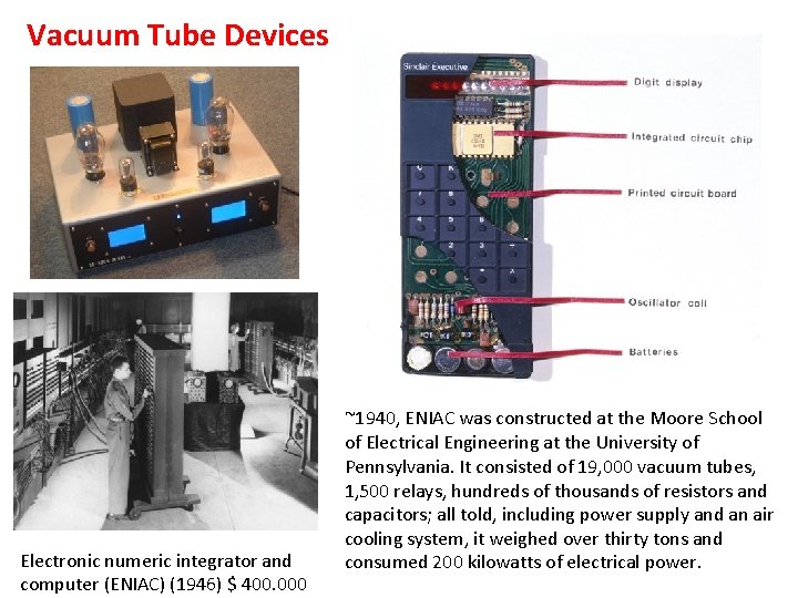
Vacuum Tube Devices ~1940, ENIAC was constructed at the Moore School Electronic numeric integrator and computer (ENIAC) (1946) $ 400. 000 of Electrical Engineering at the University of Pennsylvania. It consisted of 19, 000 vacuum tubes, 1, 500 relays, hundreds of thousands of resistors and capacitors; all told, including power supply and an air cooling system, it weighed over thirty tons and consumed 200 kilowatts of electrical power.
Solid State Devices • Transistors (BJT, FET, etc. ) • Semiconductor materials can generate and sense light OPTOELECTRONIC DEVICES • They can also sense magnetism, temperature, pressure variety of SENSOR devices and TRANSDUCERS (energy converters) appeared on the market.
• Although semiconductor diodes and transistors are still widely used as individual components, • 1959: Robert Noyce discovered that more than one transistor could be constructed on a single piece of semiconductor material. • Then other components (resistors, capacitors, etc. ) were added with transistors and then interconnected to form a complete circuit on a single chip or piece of semiconductor material. Integrated Circuit (IC) or IC Chip
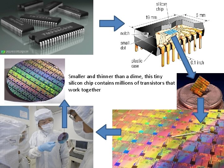
Smaller and thinner than a dime, this tiny silicon chip contains millions of transistors that work together
Steps • Growth of Semiconductor • Device Fabrication – Oxidation – Patterning (lithography, deposition, etching) • Packaging
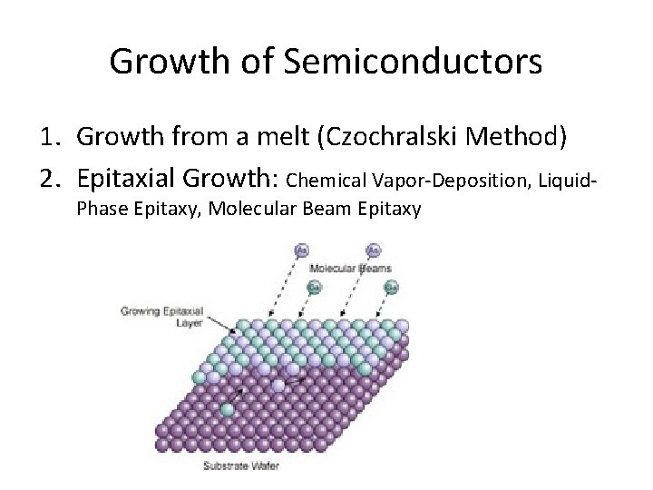
Growth of Semiconductors 1. Growth from a melt (Czochralski Method) 2. Epitaxial Growth: Chemical Vapor-Deposition, Liquid. Phase Epitaxy, Molecular Beam Epitaxy
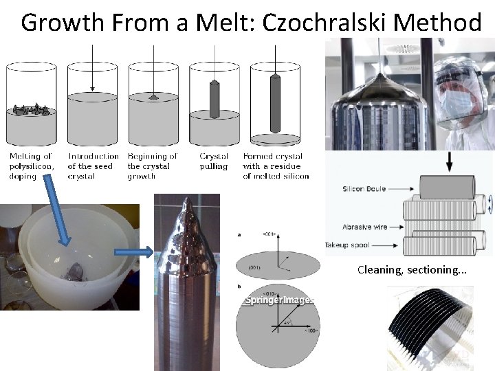
Growth From a Melt: Czochralski Method Cleaning, sectioning. . .
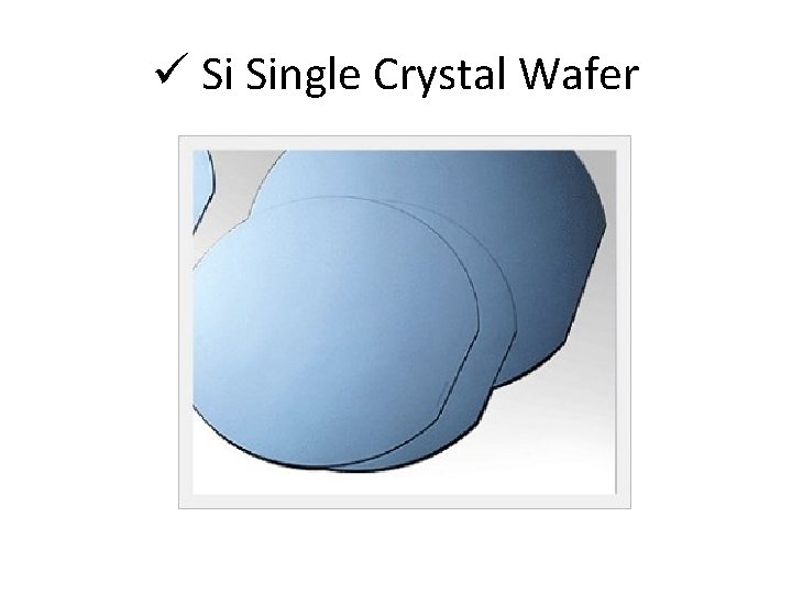
ü Si Single Crystal Wafer
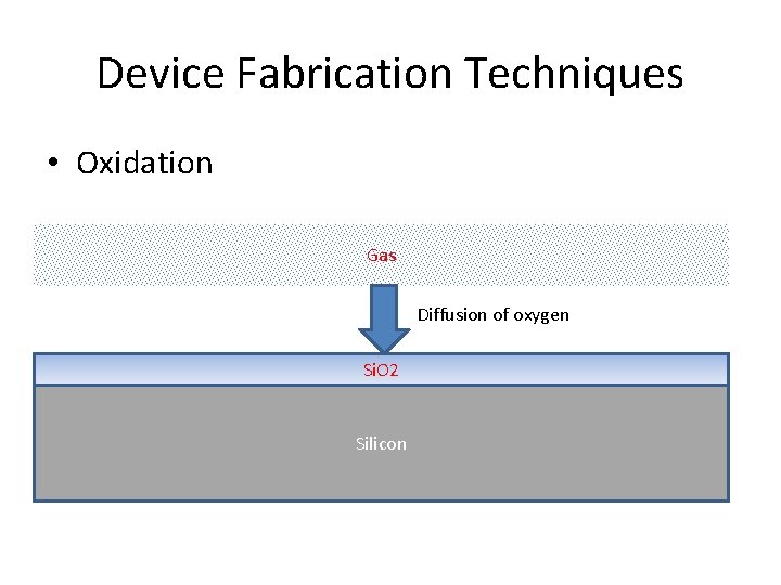
Device Fabrication Techniques • Oxidation Gas Diffusion of oxygen Si. O 2 Silicon
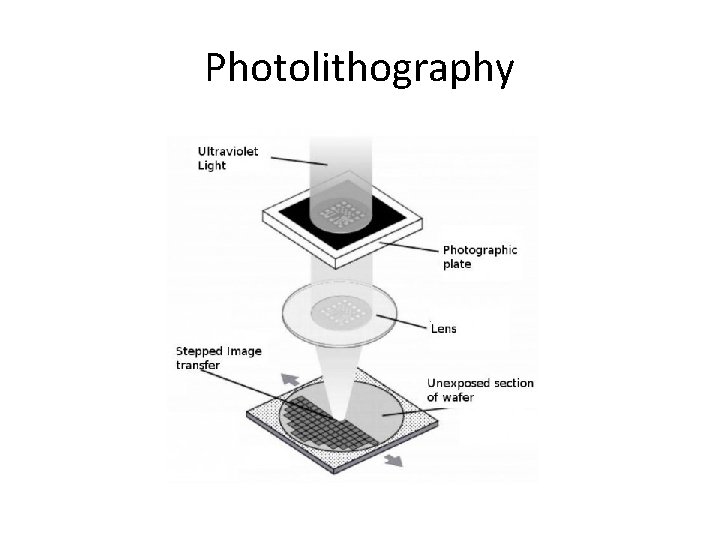
Photolithography
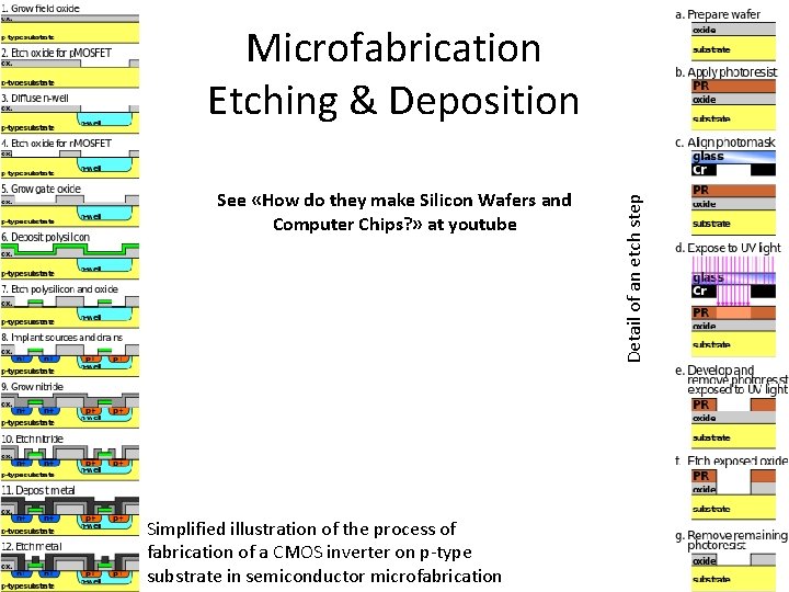
See «How do they make Silicon Wafers and Computer Chips? » at youtube Simplified illustration of the process of fabrication of a CMOS inverter on p-type substrate in semiconductor microfabrication Detail of an etch step Microfabrication Etching & Deposition
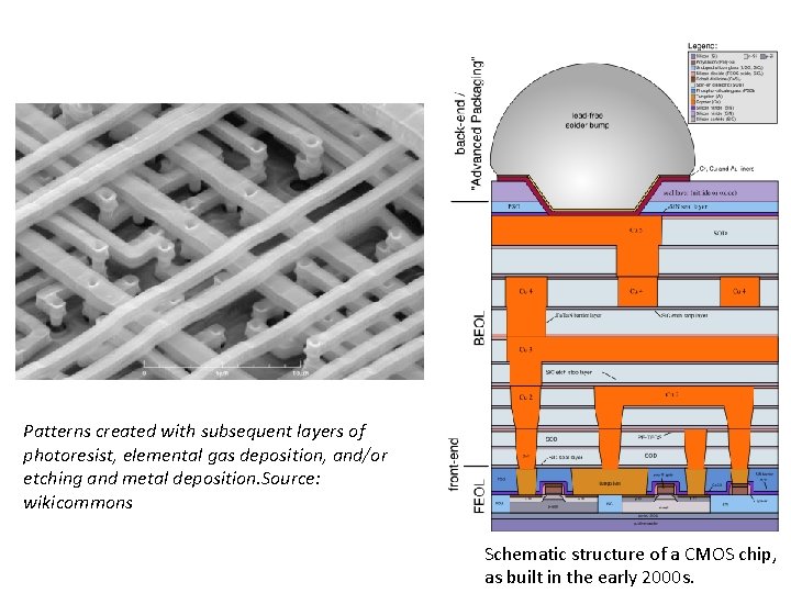
Patterns created with subsequent layers of photoresist, elemental gas deposition, and/or etching and metal deposition. Source: wikicommons Schematic structure of a CMOS chip, as built in the early 2000 s.
- Slides: 14