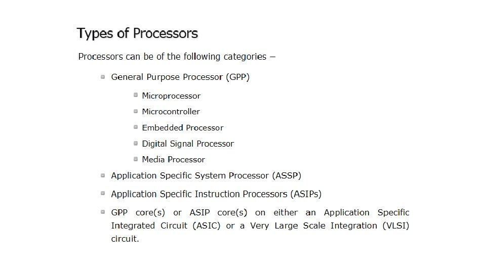
Microcontroller and Embedded Systems Lecture 2 Brief History

Microcontroller and Embedded Systems Lecture 2

Brief History of 8051 • • The first microprocessor 4004 was invented by Intel Corporation. 8085 and 8086 microprocessors were also invented by Intel. In 1981, Intel introduced an 8 -bit microcontroller called the 8051. It was referred as system on a chip because it had • 128 bytes of RAM, • 4 K byte of on-chip ROM, • two timers, • one serial port, and • 4 ports (8 -bit wide), all on a single chip. • When it became widely popular, Intel allowed other manufacturers to make and market different flavors of 8051 with its code compatible with 8051. • It means that if you write your program for one flavor of 8051, it will run on other flavors too, regardless of the manufacturer. • This has led to several versions with different speeds and amounts of onchip RAM.

Features of 8051 Microcontroller An 8051 microcontroller comes bundled with the following features − • 64 K bytes on-chip program memory (ROM) • 128 bytes on-chip data memory (RAM) • Four register banks • 128 user defined software flags • 8 -bit bidirectional data bus • 16 -bit unidirectional address bus • 32 general purpose registers each of 8 -bit • 16 bit Timers (usually 2, but may have more or less) • Three internal and two external Interrupts • Four 8 -bit ports, (short model have two 8 -bit ports) • 16 -bit program counter and data pointer • 8051 may also have a number of special features such as UARTs, ADC, Op-amp, etc. • Full duplex serial data transmitter/ receiver • On chip Oscillator and clock circuits

Block Diagram of 8051 Microcontroller

Pin Diagram 8051

• • In 8051, I/O operations are done using four ports and 40 pins. The following pin diagram shows the details of the 40 pins. I/O operation port reserves 32 pins where each port has 8 pins. The other 8 pins are designated as Vcc, GND, XTAL 1, XTAL 2, RST, EA (bar), ALE/PROG (bar), and PSEN (bar).

I/O Ports and their Functions • The four ports P 0, P 1, P 2, and P 3, each use 8 pins, making them 8 -bit ports. • Upon RESET, all the ports are configured as inputs, ready to be used as input ports. • When the first 0 is written to a port, it becomes an output. • To reconfigure it as an input, a 1 must be sent to a port.
 • It has 8 pins")
Port 0 (Pin No 32 – Pin No 39) • It has 8 pins (32 to 39). • It can be used for input or output. • Unlike P 1, P 2, and P 3 ports, we normally connect P 0 to 10 K-ohm pull-up resistors to use it as an input or output port being an open drain. • It is also designated as AD 0 -AD 7, allowing it to be used as both address and data. • ALE (Pin no 31) indicates if P 0 has address or data. • When ALE = 0, it provides data D 0 -D 7, but when ALE = 1, it has address A 0 -A 7. • In case no external memory connection is available, P 0 must be connected externally to a 10 K-ohm pull-up resistor.
")
Port 0 (Pin No 32 – Pin No 39)
 • • It is an 8 -bit port")
Port 1 (Pin 1 through 8) • • It is an 8 -bit port (pin 1 through 8) and can be used either as input or output. It doesn't require pull-up resistors because they are already connected internally. Upon reset, Port 1 is configured as an input port. The following code can be used to send alternating values of 55 H and AAH to Port 1.
 If Port 1 is configured to be used")
Port 1 (Pin 1 through 8) If Port 1 is configured to be used as an output port, then to use it as an input port again, program it by writing 1 to all of its bits as in the following code.
 • Port 2 occupies a total of 8")
Port 2 (Pin 21 through 28) • Port 2 occupies a total of 8 pins (pins 21 through 28) and • can be used for both input and output operations. • Just as P 1 (Port 1), P 2 also doesn't require external Pull-up resistors because they are already connected internally. • It must be used along with P 0 to provide the 16 -bit address for the external memory. • So it is also designated as (A 0–A 7), as shown in the pin diagram. • When the 8051 is connected to an external memory, it provides path for upper 8 -bits of 16 bits address, and it cannot be used as I/O. • Upon reset, Port 2 is configured as an input port. • The following code can be used to send alternating values of 55 H and AAH to port 2.
")
Port 2 (Pin 21 through 28)
 If Port 2 is configured to be used")
Port 2 (Pin 21 through 28) If Port 2 is configured to be used as an output port, then to use it as an input port again, program it by writing 1 to all of its bits as in the following code.
 • It is also of 8 bits and")
Port 3 (Pin 10 through 17) • It is also of 8 bits and can be used as Input/Output. • This port provides some extremely important signals. • P 3. 0 and P 3. 1 are Rx. D (Receiver) and Tx. D (Transmitter) respectively and are collectively used for Serial Communication. • P 3. 2 and P 3. 3 pins are used for external interrupts. • P 3. 4 and P 3. 5 are used for timers T 0 and T 1 respectively. • P 3. 6 and P 3. 7 are Write (WR) and Read (RD) pins. • These are active low pins, means they will be active when 0 is given to them and these are used to provide Read and Write operations to External ROM in 8031 based systems.
")
Port 3 (Pin 10 through 17)

Dual Role of Port 0 and Port 2 Dual role of Port 0 − Port 0 is also designated as AD 0–AD 7, as it can be used for both data and address handling. While connecting an 8051 to external memory, Port 0 can provide both address and data. The 8051 microcontroller then multiplexes the input as address or data in order to save pins. Dual role of Port 2 − Besides working as I/O, Port P 2 is also used to provide 16 -bit address bus for external memory along with Port 0. Port P 2 is also designated as (A 8– A 15), while Port 0 provides the lower 8 -bits via A 0–A 7. In other words, we can say that when an 8051 is connected to an external memory (ROM) which can be maximum up to 64 KB and this is possible by 16 bit address bus because we know 216 = 64 KB. Port 2 is used for the upper 8 -bit of the 16 bits address, and it cannot be used for I/O and this is the way any Program code of external ROM is addressed.

Architectural block diagram

• It consists of a Central Processing Unit • Two kinds of memory (data RAM plus program ROM/EPROM) Input/Output ports • The mode status, and data registers and random logic needed for a variety of peripheral functions. • These elements communicate through an eight bit data bus which runs throughout the chip referred as internal data bus. This bus is buffered to the outside world through an I/O port when memory or I/O expansion is desired.
: • eight-bit Arithmetic and Logic unit with associated")
• Central Processing Unit (CPU): • eight-bit Arithmetic and Logic unit with associated registers like A, B, PSW, SP • the sixteen bit program counter and “Data pointer” (DPTR) registers. • ALU: • perform arithmetic and logic functions on eight bit variables. • The arithmetic unit can perform addition, subtraction, multiplication and division. • The logic unit can perform logical operations such as AND, OR, and Exclusive-OR, as well as rotate, clear, and complement. • The ALU also looks after the branching ‘decisions. An important and unique feature of the Intel 8051 Architecture and 8031 Architecture is that the ALU can also manipulate one bit as well as eight-bit data types. Individual bits may be set, cleared, complemented, moved, tested, and used in logic computation.

Accumulator: • It is an 8 -bit register. • It holds a source operand receives the result of the arithmetic instructions (addition, subtraction, multiplication, and division). • The accumulator can be the source or destination for logical operations and a number of special data movement instructions, including look-up tables and external RAM expansion. • Several functions apply exclusively to the accumulator : rotate, parity computation, testing for zero, and so on. • In addition to accumulator, an 8 -bit B-register is available as a general purpose register when it is not being used for the hardware multiply/divide operation.
")
Program Status Word: • Many instructions implicitly or explicitly affect (or are affected by) several status flags, which are grouped together to form the Program Status Word. • It is an 8 -bit word, containing the information as follows.

Other CPU Registers: • Stack Pointer : • The stack pointer register is 8 bit wide. • It is incremented before data is stored during PUSH and ALL instructions. • The stack array can reside anywhere in on-chip RAM. • The stack pointer is initialized to 07 H after a reset. This causes the stack to begin at location 08 H. • Data Pointer (DPTR) : • The data pointer (DPTR) consists of a high byte (DPH) and a low byte (DPL). • Its function is to hold a 16 bit address. • It may be manipulated as a 16 bit data register or as two independent 8 bit registers. • It serves as a base register in indirect jumps, lookup table instructions and external data transfer.

• Memory Organization: • It can access upto 64 K program memory and 64 K data memory. • The 8051 has 4 Kbytes of internal program memory and 256 bytes of internal data memory. • Each memory type has different addressing mechanism, different control signals, and a different function. • Each may be added independently, and each uses the same address and data buses, but with different control signals. •

Memory Structure of 8051

Program Memory : • when the EA pin is connected to Vcc, program fetches to addresses 0000 H through OFFFH are directed to the internal ROM and program fetches to addresses 1000 H through FFFFH are directed to external ROM/EPROM. • On the other hand when EA pin is grounded, all addresses (0000 H to FFFFH) fetched by program are directed to the external ROM/EPROM.

Accessing External Program Memory • The PSEN signal is used to activate output enable signal of the external ROM/EPROM • The port 0 is used as a multiplexed address/data bus. • It gives lower order 8 -bit address in the initial T-cycle and later it is used as a data bus. • The 8 -bit address is latched using external latch and ALE signal generated by Intel 8051 Architecture. • The port 2 provides the higher order 8 -bit address.

Accessing External Program Memory

Timing Waveforms for External Program Memory read cycle

Interrupt /Vector locations in the lower part of program memory • The lower part of program memory stores the vector addresses for various interrupt service routines. • Each interrupt is assigned with a fixed location in program memory. • If interrupt is going to be used, its service routine must begin at corresponding location. If the interrupt is not going to be used, its service location is available as general purpose program memory. • For example, • external interrupt 0 is assigned to location 0003 H. • The interrupt service locations are spaced at 8 -byte intervals such as 0003 H for External Interrupt 0, • 000 BH for Timer 0, • 0013 H for External Interrupt 1, • 001 BH for Timer 1,

Interrupt /Vector locations in the lower part of program memory

Data Memory • The 8051 can address upto 64 Kbytes of external data memory. • The “MOVX” instruction is used to access the external data memory. • The internal data memory space for Intel 8051 Architecture and 8031 Architecture is divided into three blocks : • Lower 128 bytes, Upper 128 bytes and SFRs. • The upper addresses and SFRs occupy the same block of address space, 80 H through FFH, although they are physically separate entities. • The upper address space is accessible by indirect addressing only and SFRs are accessible by direct addressing only. • Lower address space can be accessed either by direct addressing or by indirect addressing.

A Map of 8051 Data Memory

Accessing External Data Memory The multiplexed address/data bus provided by port 0 is demultiplexed by external latch and ALE signal. • Port 2 gives the higher order address bus. The RD and WR signals from 8051 selects the memory read and memory write operation, respectively. •

Timing waveforms for external data memory read cycles

Timing waveforms for external data memory write cycles

In addition to the program and data memory, • there is another physical address space, some of these – • B, • SP, • PSW, • DPH and DPL registers are discussed earlier. • Others-I/O ports and peripheral function registers collectively referred as special function registers will be introduced in the next sections.

Special Function Register • 8051 uses memory mapped I/O through a set of special function registers that are implemented in the address space immediately above the 128 bytes of RAM. • All access to • the four I/O ports, • the CPU registers, • interrupt-control registers, • the timer/counter, UART, and • power control are performed through registers between 80 H and FFH.

RAM bit Address SFR Bit Address

Input Output Port • The MCS-51 family I/O port structure is extremely versatile. • The 8051 has 32 I/0 pins configured as four eight-bit parallel ports ( P 0, P 1, P 2, and P 3 ). • All four ports are bidirectional, i. e. each pin will be configured as input or output (or both) under software control. • Each port consists of a latch, an output driver, and an input buffer. • The output drives of Ports 0 and 2 and the input buffers of Port 0, are used in access to external memory. • Port 0 outputs the low order byte of the external memory address, time multiplexed with the data being written or read, Port 2 outputs the high order byte of the external memory address when the address is 16 bits wide. • Otherwise Port 2 gives the contents of special function register P 2. • All port pins of Port 3 are multi functional. • They have special functions including two external interrupts, two counter inputs, two special data lines and two timing control strobes.

Alternate Special Function of Port 3

Port 0 Bit • functional diagram of a typical bit latch and I/O buffers in each of the four ports. • The bit latch is nothing but the one bit in the port’s SFR. • It is represented as a D flip-flop. The signal “write to latch” acts as clock input for D flipflop. • The data from the internal bus is clock-in in response to a “write to latch” signal from the CPU. • The Q output or Q output after inversion from D flip-flop is connected at the gate input of the drive FET. • The On and OFF state of the drive FET due to the data available at the output of latch decides the status of the output pin. • It is possible to read Q output of latch by activating “read latch” signal from the CPU. • The actual port status can be read by activating “read pin” signal,

Port 0 Bit

for Port 0 and Port 2 drivers are switchable to internal ADDR/DATA and ADDR bus, respectively, by internal CONTROL signal. The switching is required to access external memory. During external memory acceses, the P 2 SFR remains unchanged, but P 0 SFR gets is written to it.

Port 1 Bit

• Port 3 has multifunction pins. • Each pin of Port 3 can be programmed to use as I/O or as one of the alternate function. • This is achieved by the another control input, “Alternate output function’, • When latch bit of Port 3 contains 1, the output level is controlled by control input, “alternate output function. ”

Port 2 Bit

• The port pin can be configured as an input by writing 1 in the latch bit of the corresponding pin. • It turn OFF the output driver FET. Then for, Ports 1, 2 and 3, the pin is pulled high by the internal pull-up, but can be pulled low by an external source. • There is no internal pull-up for port 0. Therefore, its output pin floats when 1 is written in the latch bit, and pin can be used as a high impedance input. The port. 0 is said to be “true bidirectional“, because when configured as an input it floats. • On the otherhand, the output of Ports 1, 2 and 3 are pulled high with pullup registers, when configured as an input. Thus they are sometimes called “quasi bidirectional” ports. .

Port 3 bit
 of 8051 Microcontroller NOTE: The External Access Pin (EA Pin) must")
Program Memory (ROM) of 8051 Microcontroller NOTE: The External Access Pin (EA Pin) must be pulled HIGH i. e. when the EA Pin is high, the CPU first fetches instructions from the Internal Program Memory in the address range of 0000 H to 0 FFFFH and if the memory addresses exceed the limit, then the instructions are fetched from the external ROM in the address range of 1000 H to FFFFH.

NOTE: Ignore the Internal ROM and fetch all the instructions only from the External Program Memory (External ROM). For this scenario, the EA Pin must be connected to GND. In this case, the memory addresses of the external ROM will be from 0000 H to FFFFH.
 of 8051 Microcontroller")
Data Memory (RAM) of 8051 Microcontroller

• The Data Memory or RAM of the 8051 Microcontroller stores temporary data and intermediate results that are generated and used during the normal operation of the microcontroller. Original Intel’s 8051 Microcontroller had 128 B of internal RAM. • The first 128 B i. e. memory addresses from 00 H to 7 FH is divided in to Working Registers (organized as Register Banks), Bit – Addressable Area and General Purpose RAM (also known as Scratchpad area). • In the first 128 B of RAM (from 00 H to 7 FH), the first 32 B i. e. memory from addresses 00 H to 1 FH consists of 32 Working Registers that are organized as four banks with 8 Registers in each Bank. • The 4 banks are named as Bank 0, Bank 1, Bank 2 and Bank 3. Each Bank consists of 8 registers named as R 0 – R 7. Each Register can be addressed in two ways: either by name or by address • To address the register by name, first the corresponding Bank must be selected. In order to select the bank, we have to use the RS 0 and RS 1 bits of the Program Status Word (PSW) Register (RS 0 and RS 1 are 3 rd and 4 th bits in the PSW Register).

Accessing External Program Memory

Timing Waveforms for External Program Memory read cycle

Accessing External Data Memory The multiplexed address/data bus provided by port 0 is demultiplexed by external latch and ALE signal. • Port 2 gives the higher order address bus. The RD and WR signals from 8051 selects the memory read and memory write operation, respectively. •

Timing waveforms for external data memory read cycles

Timing waveforms for external data memory write cycles

Interfacing External Memory with 8051 Microcontroller NOTE: A maximum of 64 B of Program Memory (ROM) and Data can be interface with the 8051 Microcontroller.

74 LS 373 D Latch • ALE is an output pin for the 8031/51 microcontroller. • ALE = 0 the 8031 uses PO for the data path • ALE = 1, it uses it for the address path. • To extract the addresses from the PO pins we connect PO to a 74 LS 373 latch and use the ALE pin to latch the address as shown in Figure • This extracting of addresses from PO is called address/data demultiplexing.

74 LS 373 D Latch • To extract the addresses from the PO pins we connect PO to a 74 LS 373 latch and use the ALE pin to latch the address as shown in Figure • This extracting of addresses from PO is called address/data demultiplexing.

NOTE: ALE = 0, and PO is used as a data bus, sending data out or bringing data in. Whenever the 8031/51 wants to use PO as an address bus, it puts the addresses AO – A 7 on the PO pins and activates ALE = 1 to indicate that PO has the addresses.

Data, Address, and Control Buses for the 8031
 • Another important signal for the 8031/51 is the PSEN")
PSEN (program store enable) • Another important signal for the 8031/51 is the PSEN signal. PSEN is an output signal for the 8031/51 microcontroller • Must be connected to the OE pin of a ROM containing the program code. • In other words, to access external ROM containing program code, the 8031/51 uses the PSEN signal. It is important to emphasize the role of EA and PSEN when connecting the 8031/51 to external ROM.

When the EA pin is connected to GND, the 8031/51 fetches opcode from external ROM by using PSEN. The connection of the PSEN pin to the OE pin of ROM. In systems based on the 8751/89 C 51/DS 5000 where EA is connected to VCC, these chips do not activate the PSEN pin. This indicates that the on-chip ROM contains program code.

On-chip and off-chip code ROM On-chip and Off-chip Program Code Access
 Interfacing INTERFACING OF ROM/EPROM TO µC")
MEMORY AND I/O INTERFACING External ROM (program memory) Interfacing INTERFACING OF ROM/EPROM TO µC 8051
 Interfacing INTERFACING OF RAM(DATA MEMORY) TO µC 8051.")
External RAM (data memory) Interfacing INTERFACING OF RAM(DATA MEMORY) TO µC 8051.

LINEAR AND ABSOLUTE DECODING Absolute Decoding all higher address lines : decoded to select memory chip for specific logic levels. for other logic levels memory chip is disabled. generally used in large memory systems. figure below shows memory interfacing using absolute decoding.
 INTERFACING USING ABSOLUTE DECODING.")
MEMORY (RAM) INTERFACING USING ABSOLUTE DECODING.
 for small systems : individual higher order address lines used")
Linear Decoding (Partial Decoding) for small systems : individual higher order address lines used to select memory chip. Reducing the cost of decoding, drawback is- multiple addresses. as shown in figure below, A 14 line is directly connected to chip select line, A 15 line not connected anywhere, kept open. so, status of A 15 not considered for generation of chip select signal.
 INTERFACING USING LINEAR DECODING")
MEMORY (RAM) INTERFACING USING LINEAR DECODING

Solved Examples: Example 1: Design a µController system using 8051. Interface the external RAM of size 16 k x 8.
 INTERFACING TO µC 8051")
16 K X 8 MEMORY (RAM) INTERFACING TO µC 8051

Example 2: Design a µController system using 8051. Interface the external ROM of size 4 k x 8.
 INTERFACING TO µC 8051.")
4 K X 8 MEMORY (ROM) INTERFACING TO µC 8051.

Example 3: Design a µController system using 8051, 16 k bytes of ROM & 32 k bytes of RAM. Interface the memory such that starting address for ROM is 0000 H & RAM is 8000 H.

Example 3 cont…. Memory size- RAM : 32 k that means we require 2 n=32 k : : n address lines here n=15 : : A 0 to A 14 address lines are required.

Example 3 cont….

Example 3 cont…. 16 K X 8 ROM AND 32 K X 8 RAM INTERFACING TO µC 8051.

Example 4: Design a µController system using 8051, 8 k bytes of program ROM & 8 k bytes of data RAM. Interface the memory such that starting address for ROM is 0000 H & RAM is E 000 H.

Example 4: cont….

Example 4: cont….

Example 4: cont…. 8 K X 8 ROM AND 8 K X 8 RAM INTERFACING TO µC 8051

Question Discuss the role of the PSEN pin in accessing on-chip and off-chip program codes.

Solution: In the process of fetching the internal on-chip program code the PSEN pin is not used and is never activated. However, PSEN is used for all external program fetches. PSEN is also used to activate the CE pin of the program ROM.

Embedded Systems - Timer/Counter • A timer is a specialized type of clock which is used to measure time intervals. A timer that counts from zero upwards for measuring time elapsed is often called a stopwatch. It is a device that counts down from a specified time interval and used to generate a time delay, for example, an hourglass is a timer. • A counter is a device that stores (and sometimes displays) the number of times a particular event or process occurred, with respect to a clock signal. It is used to count the events happening outside the microcontroller. In electronics, counters can be implemented quite easily using register-type circuits such as a flip-flop.

Difference between a Timer and a Counter Timer Counter • The register incremented for every machine cycle. • The register is incremented considering 1 to 0 transition at its corresponding to an external input pin (T 0, T 1). • Maximum count rate is 1/12 of the oscillator frequency. • Maximum count rate is 1/24 of the oscillator frequency. • A timer uses the frequency of the • A counter uses an external signal internal clock, and generates to count pulses. delay.

Timers of 8051 and their Associated Registers • The 8051 has two timers, Timer 0 and Timer 1. • They can be used as timers or as event counters. • Both Timer 0 and Timer 1 are 16 -bit wide. • Since the 8051 follows an 8 -bit architecture, each 16 bit is accessed as two separate registers of low-byte and high-byte.

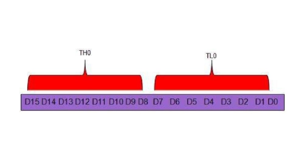
Timer 0 Register • The 16 -bit register of Timer 0 is accessed as low- and highbyte. • The low-byte register is called TL 0 (Timer 0 low byte) • The high-byte register is called TH 0 (Timer 0 high byte). • • These registers can be accessed like any other register. • For example, the instruction MOV TL 0, #4 H moves the value into the low-byte of Timer #0.

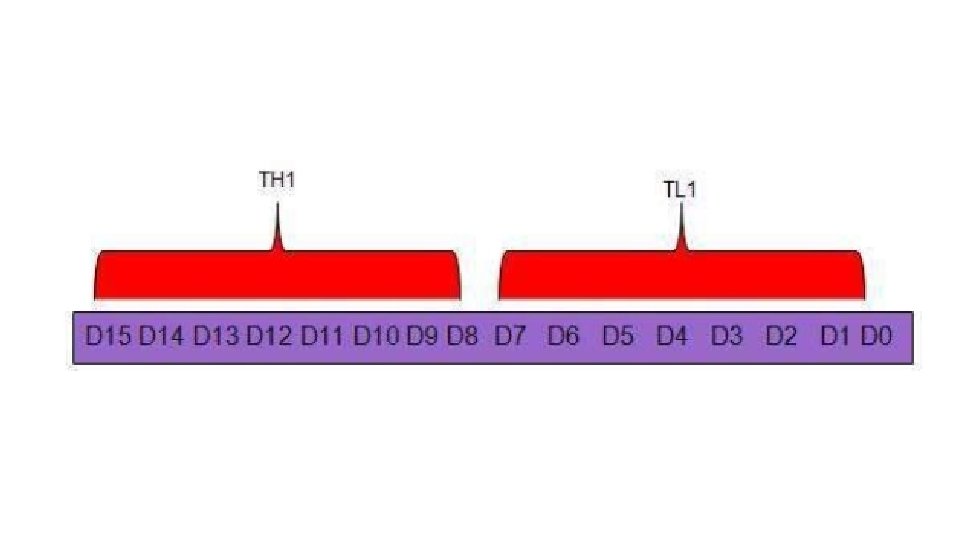
Timer 1 Register • • • The 16 -bit register of Timer 1 is accessed as low- and high-byte. The low-byte register is called TL 1 (Timer 1 low byte) The high-byte register is called TH 1 (Timer 1 high byte). These registers can be accessed like any other register. For example, the instruction MOV TL 1, #4 H moves the value into the low-byte of Timer 1.
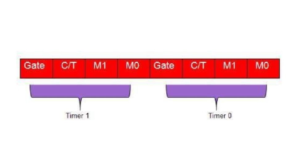
 Register • Both Timer 0 and Timer 1 use the same")
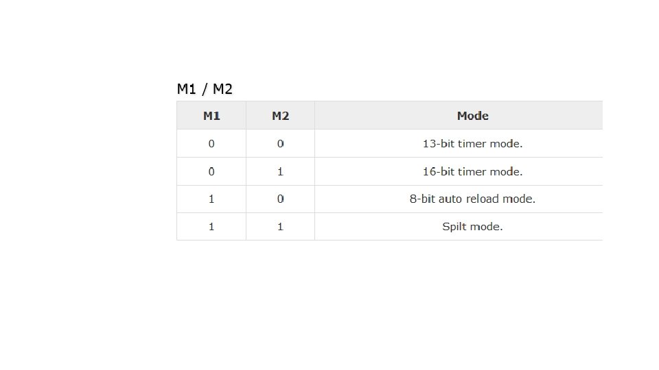
TMOD (Timer Mode) Register • Both Timer 0 and Timer 1 use the same register to set the various timer operation modes. • It is an 8 -bit register in which the lower 4 bits are set aside for Timer 0 and the upper four bits for Timers. • In each case, the lower 2 bits are used to set the timer mode in advance and the upper 2 bits are used to specify the location.
 is high. C/T")
Gate − When set, the timer only runs while INT(0, 1) is high. C/T − Counter/Timer select bit. M 1 − Mode bit 1. M 0 − Mode bit 0.

GATE Every timer has a means of starting and stopping. Some timers do this by software, some by hardware, and some have both software and hardware controls. 8051 timers have both software and hardware controls. The start and stop of a timer is controlled by software using the instruction SETB TR 1 and CLR TR 1 for timer 1, and SETB TR 0 and CLR TR 0 for timer 0. The SETB instruction is used to start it and it is stopped by the CLR instruction. These instructions start and stop the timers as long as GATE = 0 in the TMOD register. Timers can be started and stopped by an external source by making GATE = 1 in the TMOD register.
 This bit in the TMOD register is used to decide")
C/T (CLOCK / TIMER) This bit in the TMOD register is used to decide whether a timer is used as a delay generator or an event manager. If C/T = 0, it is used as a timer for timer delay generation. The clock source to create the time delay is the crystal frequency of the 8051. If C/T = 0, the crystal frequency attached to the 8051 also decides the speed at which the 8051 timer ticks at a regular interval. Timer frequency is always 1/12 th of the frequency of the crystal attached to the 8051. Although various 8051 based systems have an XTAL frequency of 10 MHz to 40 MHz, we normally work with the XTAL frequency of 11. 0592 MHz. It is because the baud rate for serial communication of the 8051. XTAL = 11. 0592 allows the 8051 system to communicate with the PC with no errors.
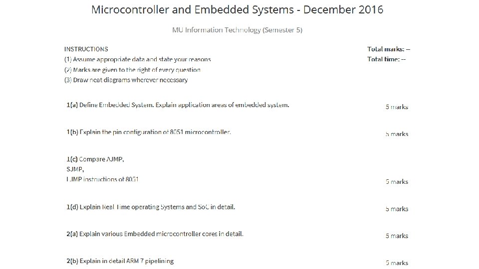
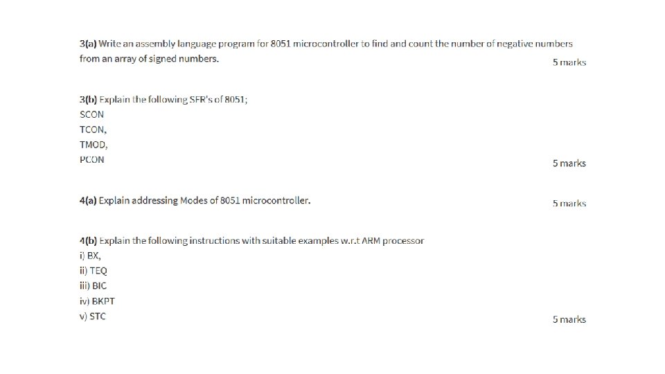
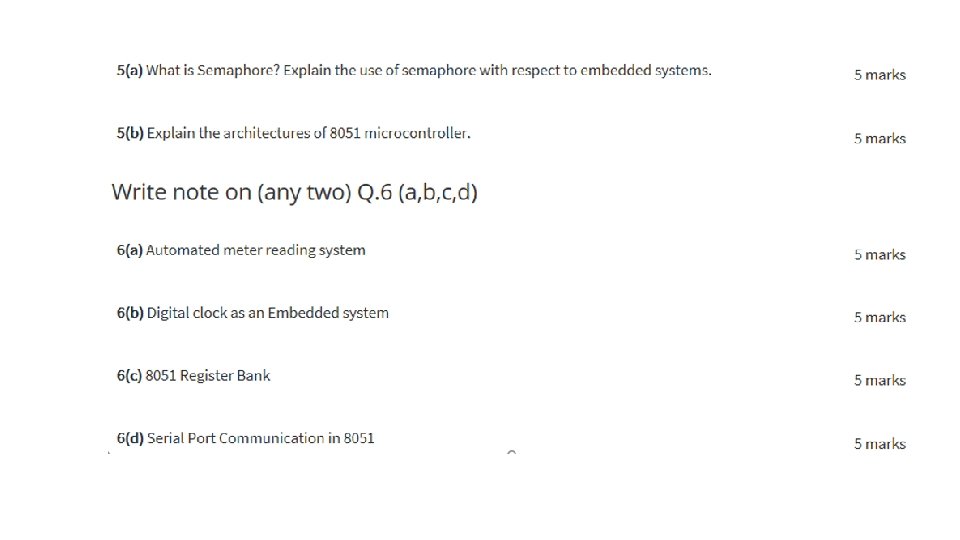

Dec 2017
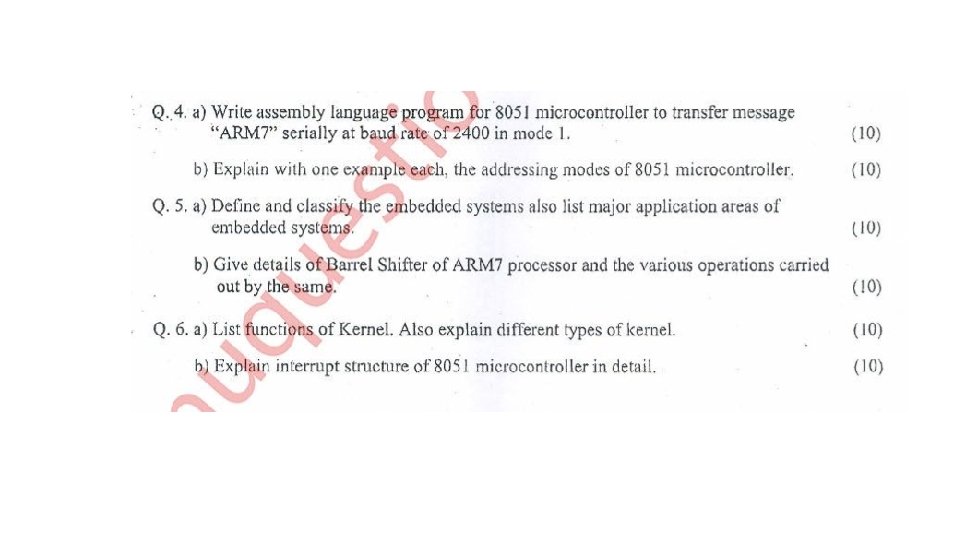

Dec 2018

May 2018
- Slides: 120