Microcomputer Based Design Lecture 05 week 04 Engr

Microcomputer Based Design Lecture #05 (week #04) Engr. Bilal Ahmad B. Tech (Electrical)
8086 Microprocessor is an enhanced version of 8085 Microprocessor that was designed by Intel in 1976. It is a 16 -bit Microprocessor having 20 address lines and 16 data lines that provides up to 1 MB storage. It consists of powerful instruction set, which provides operations like multiplication and division easily. It supports two modes of operation, i. e. Maximum mode and Minimum mode. Maximum mode is suitable for system having multiple processors and Minimum mode is suitable for system having a single processor.
Pin Diagram and Pin description of 8086 • 8086 was the first 16 -bit microprocessor available in 40 -pin chip. • Let us now discuss in detail the pin configuration of an 8086 Microprocessor.
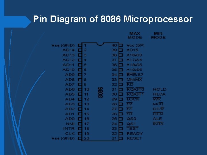
Pin Diagram of 8086 Microprocessor
Pin description of 8086 Power supply and frequency signals It uses 5 V DC supply at VCC pin 40, and uses ground at VSS pin 1 and 20 for its operation. Address/Data Bus AD 0 -AD 15. These are 16 address/data bus. AD 0 -AD 7 carries low order byte data and AD 8 AD 15 carries higher order byte data. During the first clock cycle, it carries 16 -bit address and after that it carries 16 -bit data. Clock signal is provided through Pin-19. It provides timing to the processor for operations. Its frequency is different for different versions, i. e. 5 MHz, 8 MHz and 10 MHz.
Pin description of 8086 Address/status bus A 16 -A 19/S 3 -S 6. These are the 4 address/status buses. During the first clock cycle, it carries 4 -bit address and later it carries status signals. Ready It is available at pin 22. It is an acknowledgement signal from I/O devices that data is transferred. It is an active high signal. When it is high, it indicates that the device is ready to transfer data. When it is low, it indicates wait state.

Pin description of 8086 RESET It is available at pin 21 and is used to restart the execution. It causes the processor to immediately terminate its present activity. This signal is active high for the first 4 clock cycles to RESET the microprocessor. Power supply and frequency signals It uses 5 V DC supply at VCC pin 40, and uses ground at VSS pin 1 and 20 for its operation.
Pin description of 8086 INTR It is available at pin 18. It is an interrupt request signal, which is sampled during the last clock cycle of each instruction to determine if the processor considered this as an interrupt or not. NMI It stands for non-maskable interrupt and is available at pin 17. It is an edge triggered input, which causes an interrupt request to the microprocessor.
Pin description of 8086 ALE It stands for address enable latch and is available at pin 25. A positive pulse is generated each time the processor begins any operation. This signal indicates the availability of a valid address on the address/data lines. DEN It stands for Data Enable and is available at pin 26. It is used to enable Transreceiver 8286. The transreceiver is a device used to separate data from the address/data bus. DT/R It stands for Data Transmit/Receive signal and is available at pin 27. It decides the direction of data flow through the transreceiver. When it is high, data is transmitted out and vice-a-versa.
Pin description of 8086 M/IO This signal is used to distinguish between memory and I/O operations. When it is high, it indicates I/O operation and when it is low indicates the memory operation. It is available at pin 28. WR It stands for write signal and is available at pin 29. It is used to write the data into the memory or the output device depending on the status of M/IO signal. HLDA It stands for Hold Acknowledgement signal and is available at pin 30. This signal acknowledges the HOLD signal. HOLD This signal indicates to the processor that external devices are requesting to access the address/data buses. It is available at pin 31.

Thank You
- Slides: 11