Micro Pixel Chamber mPIC PCB technology Pixel electrode
 • PCB technology • Pixel electrode • 2 D readout")
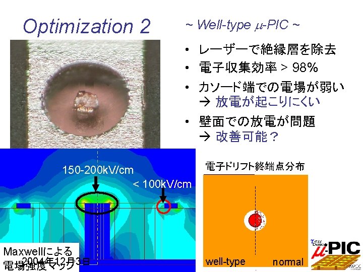
Micro Pixel Chamber (m-PIC) • PCB technology • Pixel electrode • 2 D readout 100 mm • 400 m pitch electrodes • 256 anodes and 256 cathodes 2004年 12月3日 10 cm Detection area = 100 cm 2

Performance of m-PIC 0. 5 mm slits 103 400 (8 0 2 H 6 A /C C / r Ar 104 Max: 1. 6× 10⁴ ) 0 /1 0 9 ( 6 H 2 /2 0) Gas gain Anode voltage [V] Max: 1. 6× 10⁴ Gas gain Stable: ~6000 2004年 12月3日 Max gas gain … position resolution limited by discharge σ=120 m Length along the edge [mm]

Simulation 3 D simulation using MAXWELL and GARFIELD • MAXWELL – 3 D structure – Finite element method • GARFIELD – Electron drift – Gas multiplication MAXWELL 2004年 12月3日 Field map GARFIELD Expected performance
 2. Malter effect")
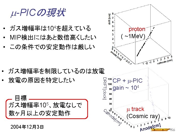
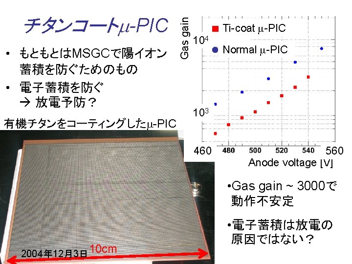
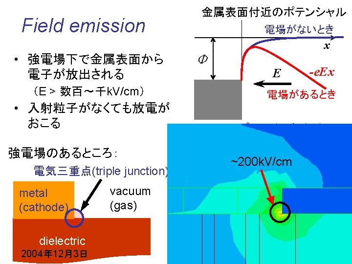
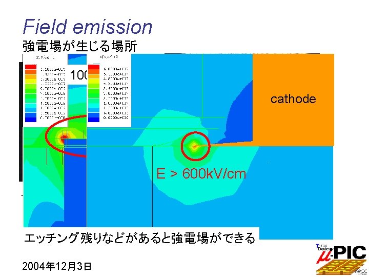
Discharge Possible mechanism … 1. High ionization (avalanche size >108 electrons) 2. Malter effect (ポリマー膜の絶縁破壊) 3. 絶縁層への電子の蓄積 帯電 沿面放電 4. カソード端からのField emission Damaged electrode of MSGC 10 m 電子収集効率 ~90% ~10% (anode) 10 m Damaged electrode (cathode) (anode) charging-up 2004年 12月3日 電子ドリフト終端点分布 Nagae et al. , NIM A 323 (1992) 236
![Emitted electrons ~ Case of the current m-PIC ~ E field [k. V/cm] Townsend](http://slidetodoc.com/presentation_image_h2/ae8580a99a07cd46659928d609caf347/image-11.jpg "Emitted electrons ~ Case of the current m-PIC ~ E field [k. V/cm] Townsend")
Emitted electrons ~ Case of the current m-PIC ~ E field [k. V/cm] Townsend [1/cm] 基板表面に沿ったTownsend係数 基板表面に沿った電場強度 180 104 103 1002 10 10 20 Surface flashover Triple junction 2004年 12月3日 TJからField emission 基板表面を走りながら ガス増幅 基板表面に沿って Townsend係数を積分 “ガス増幅率” ~ 5× 10⁷ Raether limitに近い
![Optimization 1 E field [k. V/cm] 350 Thickness 5 m 100 m 200 m](http://slidetodoc.com/presentation_image_h2/ae8580a99a07cd46659928d609caf347/image-13.jpg "Optimization 1 E field [k. V/cm] 350 Thickness 5 m 100 m 200 m")
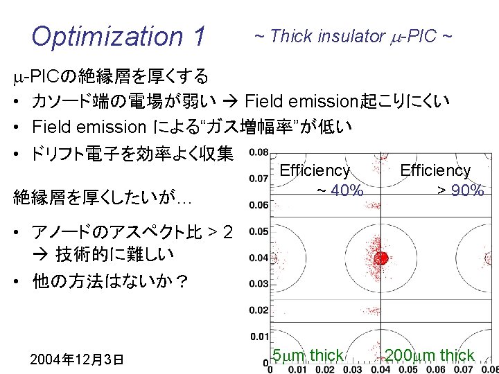
Optimization 1 E field [k. V/cm] 350 Thickness 5 m 100 m 200 m ~ Thick insulator m-PIC ~ Thick insulator High field @ anode Low field @ cathode • High gas gain ( > 105) 100 • Discharge-free operation r O anode (600 V) 2004年 12月3日 cathode (GND)

Optimization 1 ~ Thick insulator m-PIC ~ current -PIC 基板表面を走る電子の”ガス増幅” Multiplication 1010 109 Triple junction 108 Raether limit 沿面ガス増幅率の厚さ依存 (これは前頁?) 107 106 薄い基板: 沿面放電の”ガス増幅率” がRaether limitを超える 沿面フラッシオーバ? 50 100 2004年 12月3日 150 200 Thickness [ m]
- Slides: 17