Michael Fuhrer Director FLEET Monash University 24 th

- Slides: 44

Michael Fuhrer Director, FLEET Monash University 24 th Canberra International Physics Summer School – Topological Matter Lecture 2

Aims of this lecture series • Introduce electronic transport measurements • What do we measure? • How do we interpret the measurements? • What are (some of) the signatures of topology in electronic transport? • 2 D topological insulators • Quantum Hall effect and the “edge state picture” • Quantum spin Hall effect • Interpreting conductance within Landauer-Buttiker formalism and edge state picture • 2 D Dirac surface state of 3 D TIs • • • Graphene as an example of a 2 D Dirac system Conductivity of a disordered 2 D Dirac system Non-linear screening and electron-hole “puddling” 2 D Dirac surface state of a 3 D time-reversal symmetric TI Weak localization and weak anti-localization Landau levels of the 2 D Dirac system

Graphene

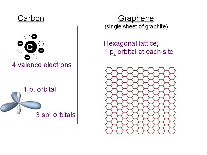
Carbon Graphene (single sheet of graphite) - C - 4 valence electrons 1 pz orbital 3 sp 2 orbitals Hexagonal lattice; 1 pz orbital at each site

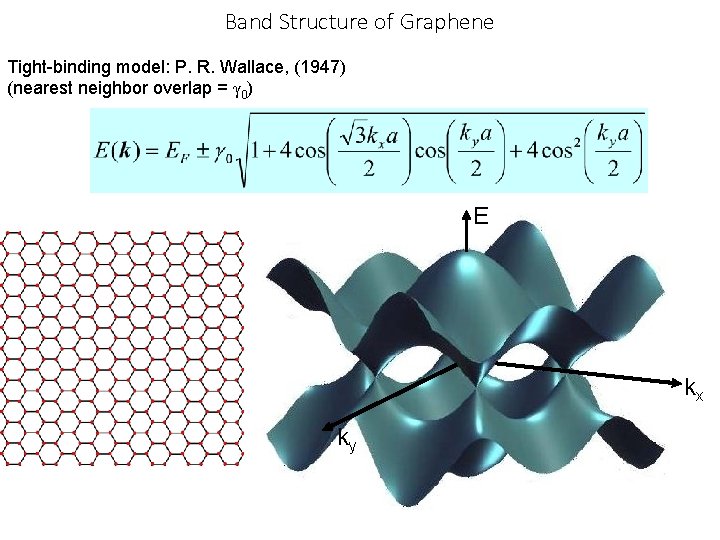
Band Structure of Graphene Tight-binding model: P. R. Wallace, (1947) (nearest neighbor overlap = γ 0) E kx ky

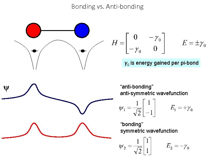
Bonding vs. Anti-bonding γ 0 is energy gained per pi-bond ψ “anti-bonding” anti-symmetric wavefunction “bonding” symmetric wavefunction

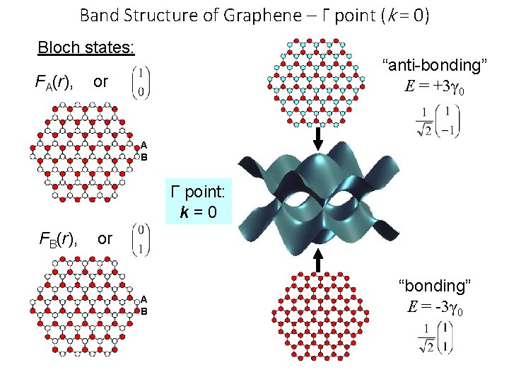
Band Structure of Graphene – Γ point (k = 0) Bloch states: FA(r), “anti-bonding” E = +3γ 0 or A B Γ point: k=0 FB(r), or A B “bonding” E = -3γ 0

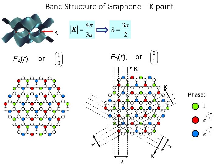
Band Structure of Graphene – K point K FB(r), or or K K Phase: λ λ FA(r), λ K

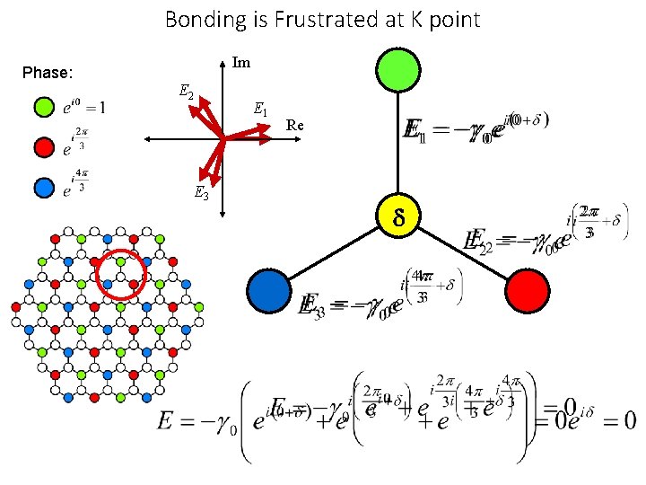
Bonding is Frustrated at K point Phase: Im E 2 E 3 E 1 Re 0 d

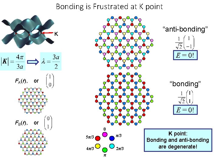
Bonding is Frustrated at K point “anti-bonding” K E = 0! FA(r), or “bonding” E = 0! FB(r), or 0 5π/3 4π/3 2π/3 π K point: Bonding and anti-bonding are degenerate!

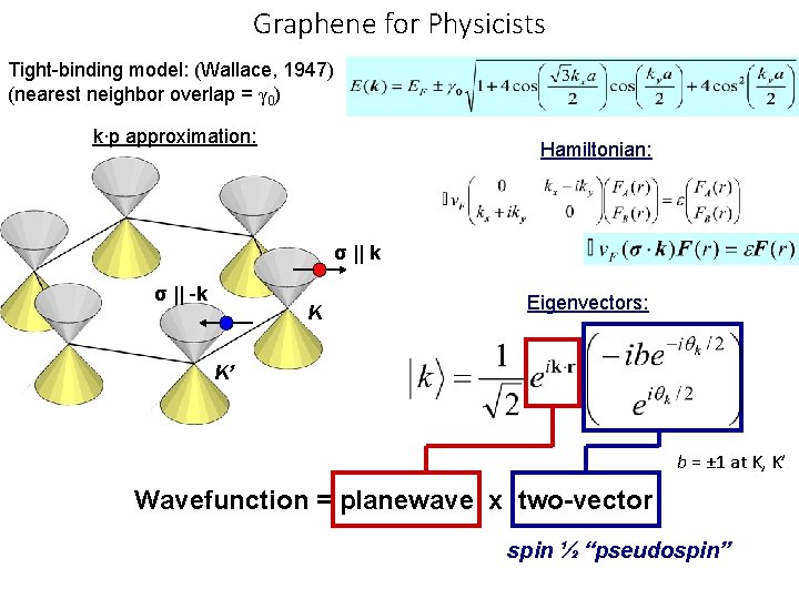
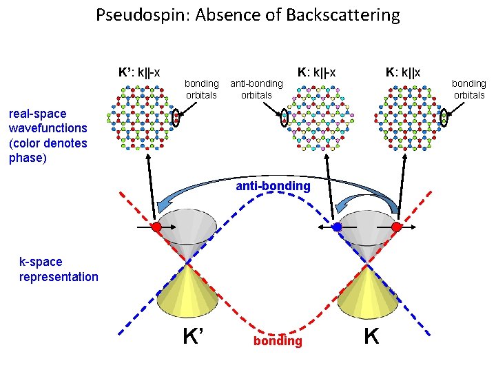
Graphene for Physicists Tight-binding model: (Wallace, 1947) (nearest neighbor overlap = γ 0) k∙p approximation: Hamiltonian: σ || k σ || -k K Eigenvectors: K’ b = ± 1 at K, K’ Wavefunction = planewave x two-vector spin ½ “pseudospin”

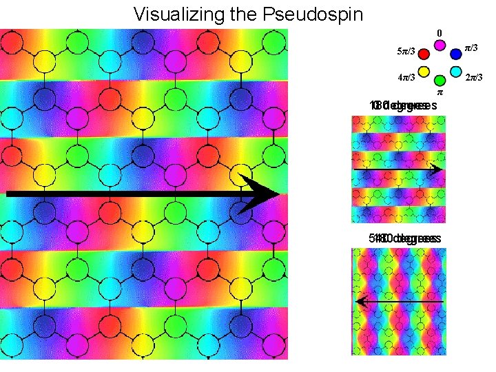
Visualizing the Pseudospin 0 5π/3 4π/3 2π/3 π 180 0 degrees 540 180 degrees

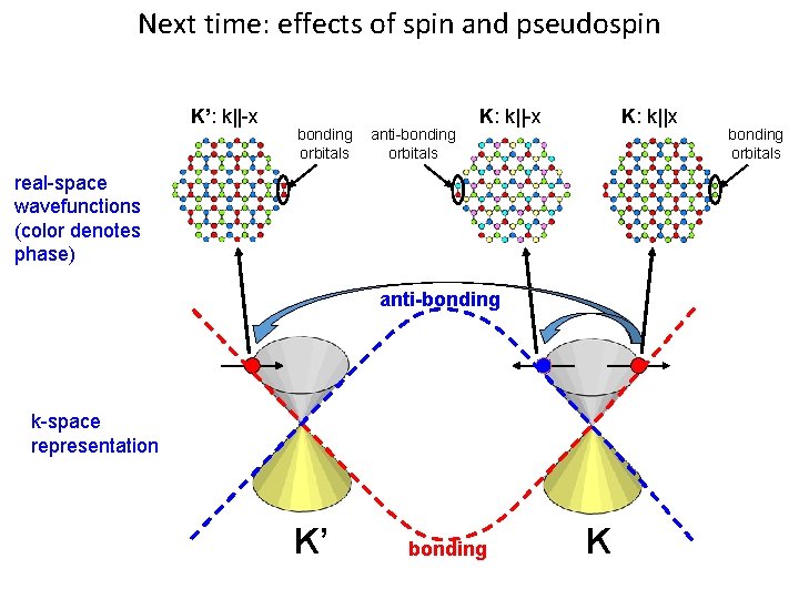
Pseudospin: Absence of Backscattering K’: k||-x bonding orbitals anti-bonding orbitals K: k||-x K: k||x real-space wavefunctions (color denotes phase) anti-bonding k-space representation K’ bonding K bonding orbitals

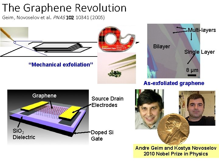
The Graphene Revolution Geim, Novoselov et al. PNAS 102 10341 (2005) Multi-layers Bilayer “Mechanical exfoliation” Single Layer 8 µm As-exfoliated graphene Graphene Si. O 2 Dielectric Source Drain Electrodes Doped Si Gate Andre Geim and Kostya Novoselov 2010 Nobel Prize in Physics

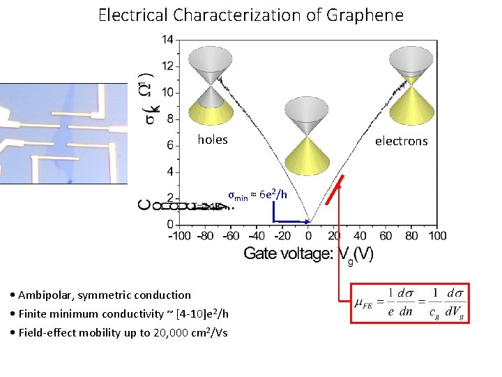
Electrical Characterization of Graphene holes electrons σmin ≈ 6 e 2/h • Ambipolar, symmetric conduction • Finite minimum conductivity ~ [4 -10]e 2/h • Field-effect mobility up to 20, 000 cm 2/Vs

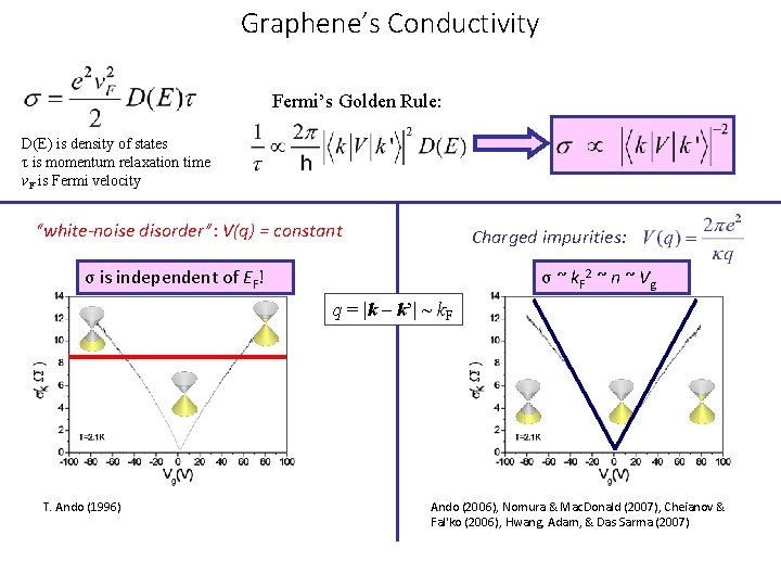
Graphene’s Conductivity Fermi’s Golden Rule: D(E) is density of states τ is momentum relaxation time v. F is Fermi velocity “white-noise disorder”: V(q) = constant Charged impurities: σ is independent of EF! σ ~ k. F 2 ~ n ~ Vg q = |k – k’| ~ k. F T. Ando (1996) Ando (2006), Nomura & Mac. Donald (2007), Cheianov & Fal'ko (2006), Hwang, Adam, & Das Sarma (2007)

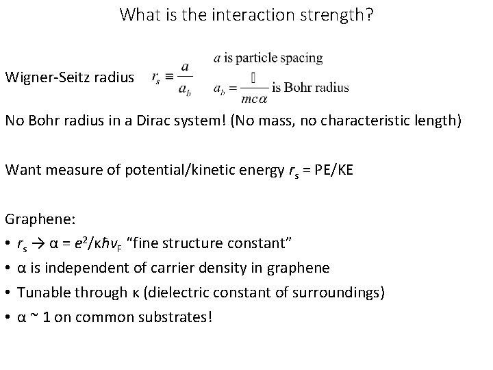
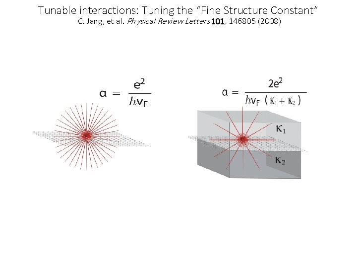
What is the interaction strength? Wigner-Seitz radius No Bohr radius in a Dirac system! (No mass, no characteristic length) Want measure of potential/kinetic energy rs = PE/KE Graphene: • rs → α = e 2/κħv. F “fine structure constant” • α is independent of carrier density in graphene • Tunable through κ (dielectric constant of surroundings) • α ~ 1 on common substrates!

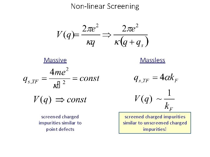
Non-linear Screening Massive screened charged impurities similar to point defects Massless screened charged impurities similar to unscreened charged impurities!

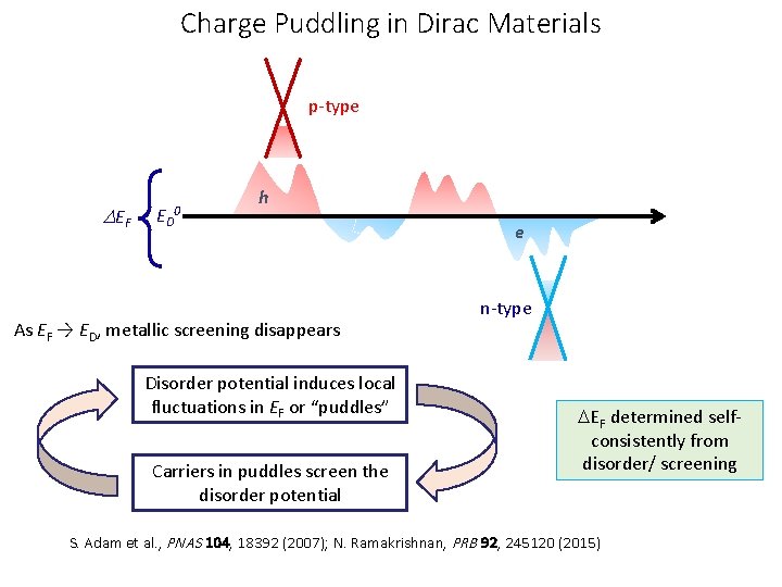
Charge Puddling in Dirac Materials p-type EF ED 0 h As EF → ED, metallic screening disappears Disorder potential induces local fluctuations in EF or “puddles” Carriers in puddles screen the disorder potential e n-type EF determined selfconsistently from disorder/ screening S. Adam et al. , PNAS 104, 18392 (2007); N. Ramakrishnan, PRB 92, 245120 (2015)

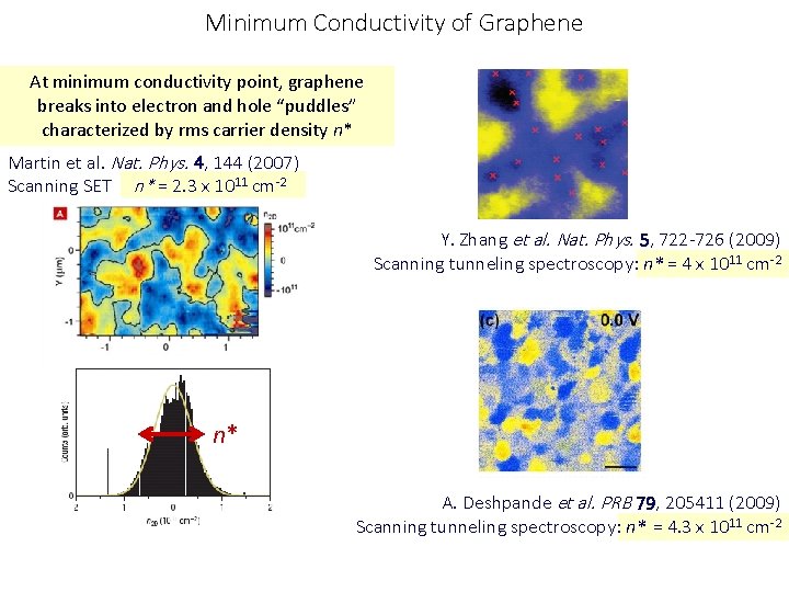
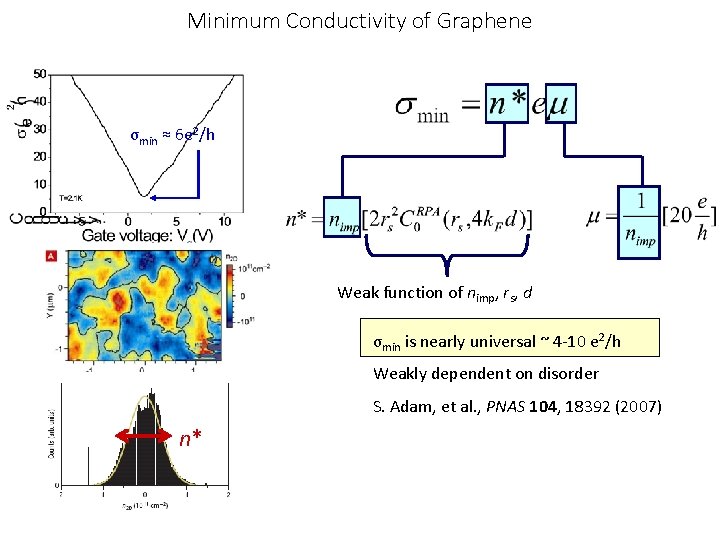
Minimum Conductivity of Graphene At minimum conductivity point, graphene breaks into electron and hole “puddles” characterized by rms carrier density n* Martin et al. Nat. Phys. 4, 144 (2007) Scanning SET n* = 2. 3 x 1011 cm-2 Y. Zhang et al. Nat. Phys. 5, 722 -726 (2009) Scanning tunneling spectroscopy: n* = 4 x 1011 cm-2 n* A. Deshpande et al. PRB 79, 205411 (2009) Scanning tunneling spectroscopy: n* = 4. 3 x 1011 cm-2

Minimum Conductivity of Graphene σmin ≈ 6 e 2/h Weak function of nimp, rs, d σmin is nearly universal ~ 4 -10 e 2/h Weakly dependent on disorder S. Adam, et al. , PNAS 104, 18392 (2007) n*

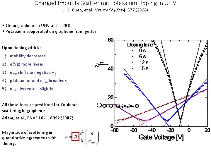
Charged Impurity Scattering: Potassium Doping in UHV J. H. Chen, et al. Nature Physics 4, 377 (2008) • Clean graphene in UHV at T = 20 K • Potassium evaporated on graphene from getter Upon doping with K: 1) mobility decreases 2) σ(Vg) more linear 3) σmin shifts to negative Vg 4) plateau around σmin broadens 5) σmin decreases (slightly) All these feature predicted for Coulomb scattering in graphene Adam, et al. , PNAS 104, 18392 (2007) Magnitude of scattering in quantitative agreement with theory:

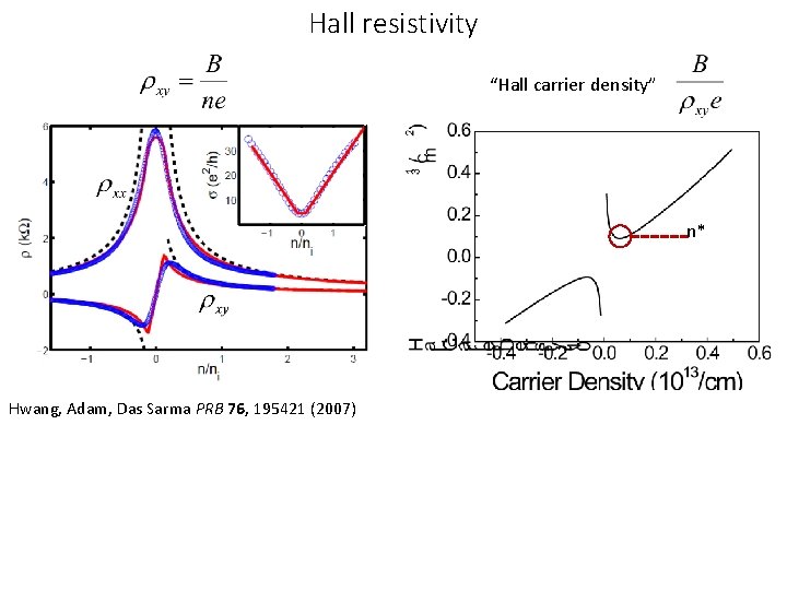
Hall resistivity “Hall carrier density” n* Hwang, Adam, Das Sarma PRB 76, 195421 (2007)

Tunable interactions: Tuning the “Fine Structure Constant” C. Jang, et al. Physical Review Letters 101, 146805 (2008)

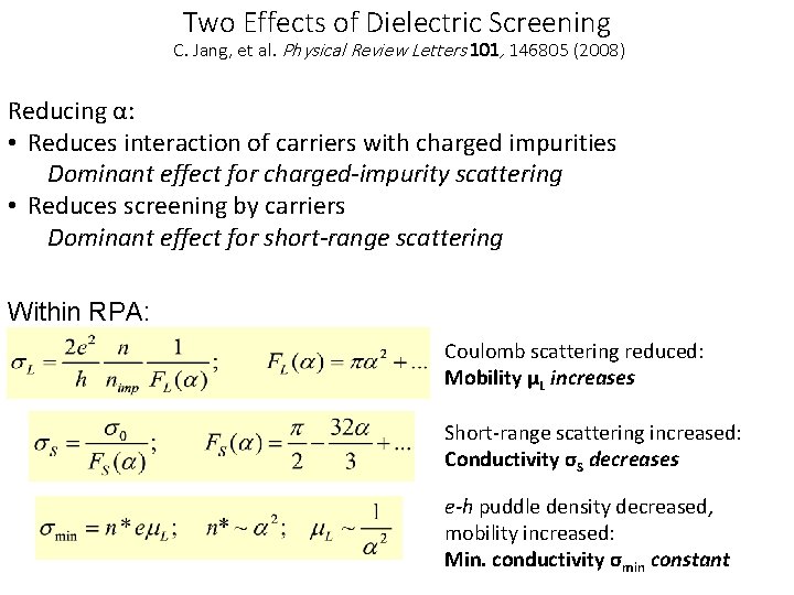
Two Effects of Dielectric Screening C. Jang, et al. Physical Review Letters 101, 146805 (2008) Reducing α: • Reduces interaction of carriers with charged impurities Dominant effect for charged-impurity scattering • Reduces screening by carriers Dominant effect for short-range scattering Within RPA: Coulomb scattering reduced: Mobility μL increases Short-range scattering increased: Conductivity σS decreases e-h puddle density decreased, mobility increased: Min. conductivity σmin constant

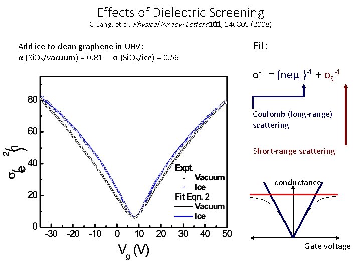
Effects of Dielectric Screening C. Jang, et al. Physical Review Letters 101, 146805 (2008) Add ice to clean graphene in UHV: α (Si. O 2/vacuum) = 0. 81 α (Si. O 2/ice) = 0. 56 Fit: σ-1 = (neμL)-1 + σS-1 Coulomb (long-range) scattering Short-range scattering conductance Gate voltage

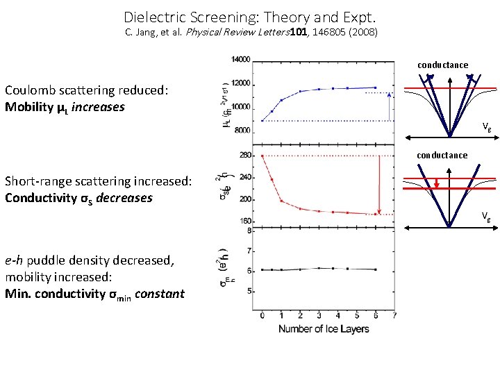
Dielectric Screening: Theory and Expt. C. Jang, et al. Physical Review Letters 101, 146805 (2008) conductance Coulomb scattering reduced: Mobility μL increases Vg conductance Short-range scattering increased: Conductivity σS decreases Vg e-h puddle density decreased, mobility increased: Min. conductivity σmin constant

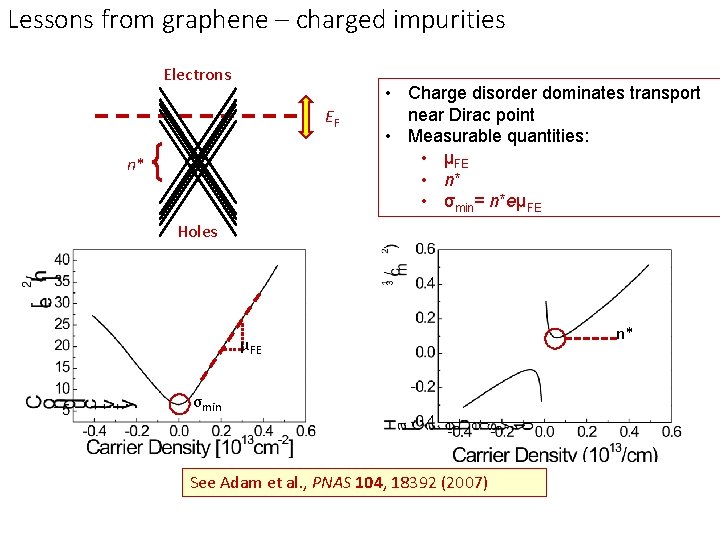
Lessons from graphene – charged impurities Electrons EF n* • Charge disorder dominates transport near Dirac point • Measurable quantities: • μFE • n* • σmin= n*eμFE Holes μFE σmin See Adam et al. , PNAS 104, 18392 (2007) n*

Time-reversal symmetric topological insulators

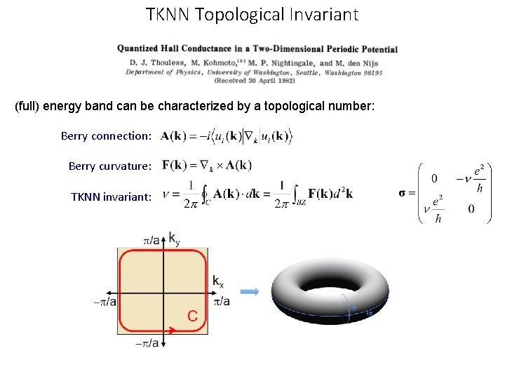
TKNN Topological Invariant (full) energy band can be characterized by a topological number: Berry connection: Berry curvature: TKNN invariant:

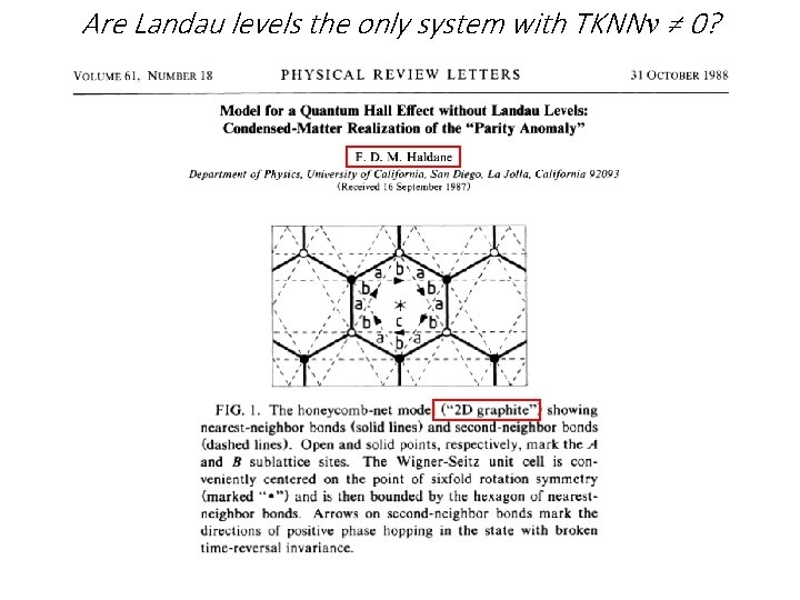
Are Landau levels the only system with TKNN ν ≠ 0?

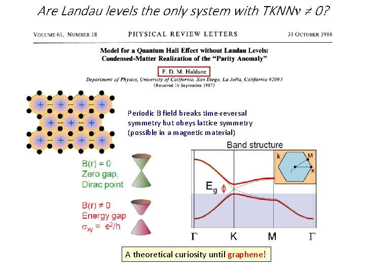
Are Landau levels the only system with TKNN ν ≠ 0? Periodic B field breaks time-reversal symmetry but obeys lattice symmetry (possible in a magnetic material) A theoretical curiosity until graphene!

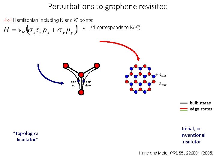
Perturbations to graphene revisited 4 x 4 Hamiltonian including K and K’ points: τ = ± 1 corresponds to K(K’) staggered sublattice potential spin-orbit coupling spin up spin down bulk states edge states “topological Insulator” trivial, or conventional insulator Kane and Mele, PRL 95, 226801 (2005)

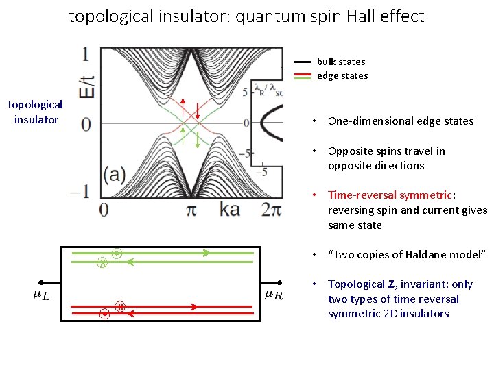
topological insulator: quantum spin Hall effect bulk states edge states topological insulator • One-dimensional edge states • Opposite spins travel in opposite directions • Time-reversal symmetric: reversing spin and current gives same state • “Two copies of Haldane model” x x • Topological Z 2 invariant: only two types of time reversal symmetric 2 D insulators

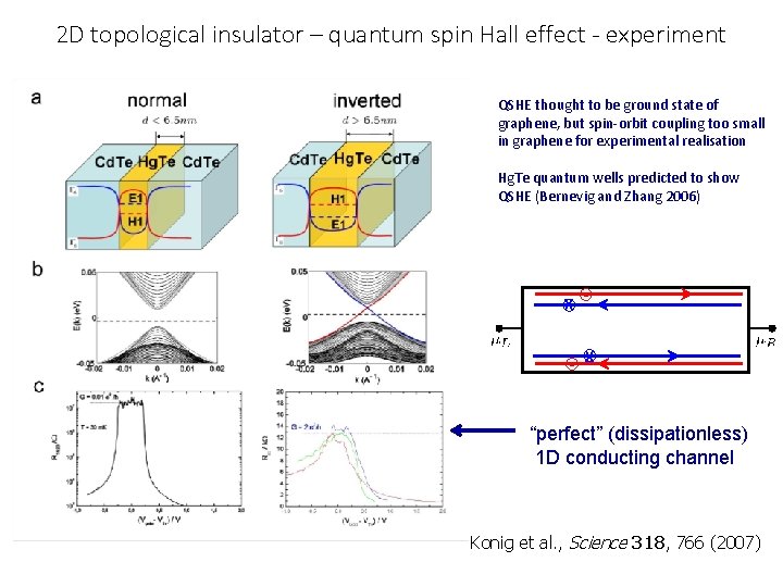
2 D topological insulator – quantum spin Hall effect - experiment QSHE thought to be ground state of graphene, but spin-orbit coupling too small in graphene for experimental realisation Hg. Te quantum wells predicted to show QSHE (Bernevig and Zhang 2006) x x “perfect” (dissipationless) 1 D conducting channel Konig et al. , Science 318, 766 (2007)

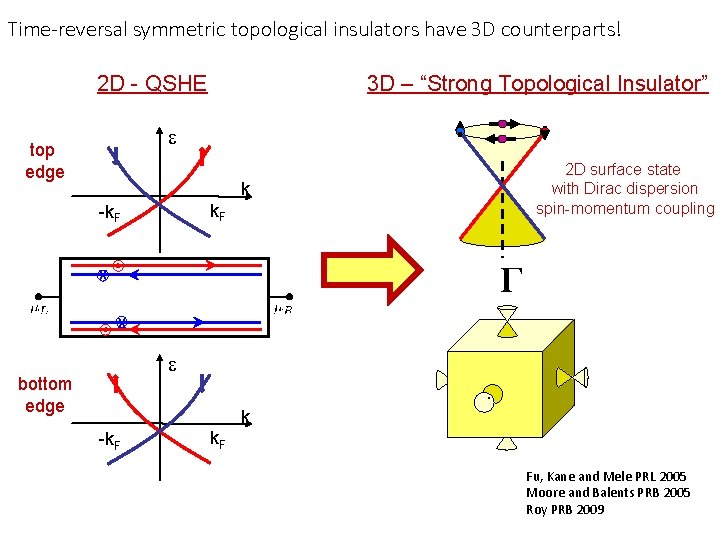
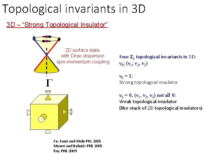
Time-reversal symmetric topological insulators have 3 D counterparts! 2 D - QSHE 3 D – “Strong Topological Insulator” e top edge 2 D surface state with Dirac dispersion spin-momentum coupling k k. F -k. F Γ x x e bottom edge k -k. F Fu, Kane and Mele PRL 2005 Moore and Balents PRB 2005 Roy PRB 2009

Topological invariants in 3 D 3 D – “Strong Topological Insulator” 2 D surface state with Dirac dispersion spin-momentum coupling Four Z 2 topological invariants in 3 D: ν 0; (ν 1, ν 2, ν 3) ν 0 = 1: Strong topological insulator Γ ν 0 = 0, (ν 1, ν 2, ν 3) not all 0: Weak topological insulator (like stack of 2 D topological insulators) Fu, Kane and Mele PRL 2005 Moore and Balents PRB 2005 Roy PRB 2009

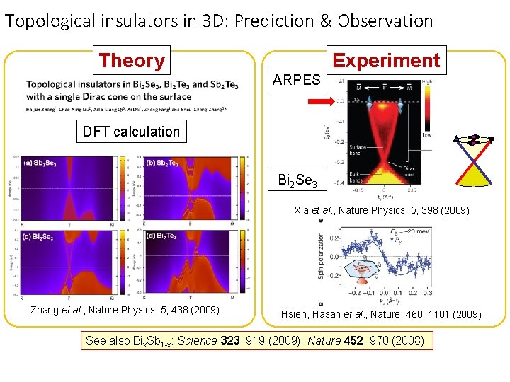
Topological insulators in 3 D: Prediction & Observation (a) Sb 2 Se 3 Theory (b) Sb. Experiment 2 Te 3 ARPES DFT calculation Bi 2 Se 3 (c) Bi 2 Se 3 Zhang et al. , Nature Physics, 5, 438 (2009) Xia et al. , Nature Physics, 5, 398 (2009) Hsieh, Hasan et al. , Nature, 460, 1101 (2009) See also Bix. Sb 1 -x: Science 323, 919 (2009); Nature 452, 970 (2008)

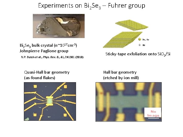
Experiments on Bi 2 Se 3 – Fuhrer group Bi 2 Se 3 bulk crystal (n~1017 cm-3) Johnpierre Paglione group N. P. Butch et al. , Phys. Rev. B. , 81, 241301 (2010) Quasi-Hall bar geometry (as-found flakes) Sticky-tape exfoliation onto Si. O 2/Si Hall bar geometry (etched by ion mill)

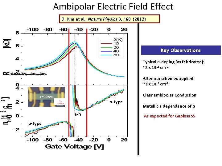
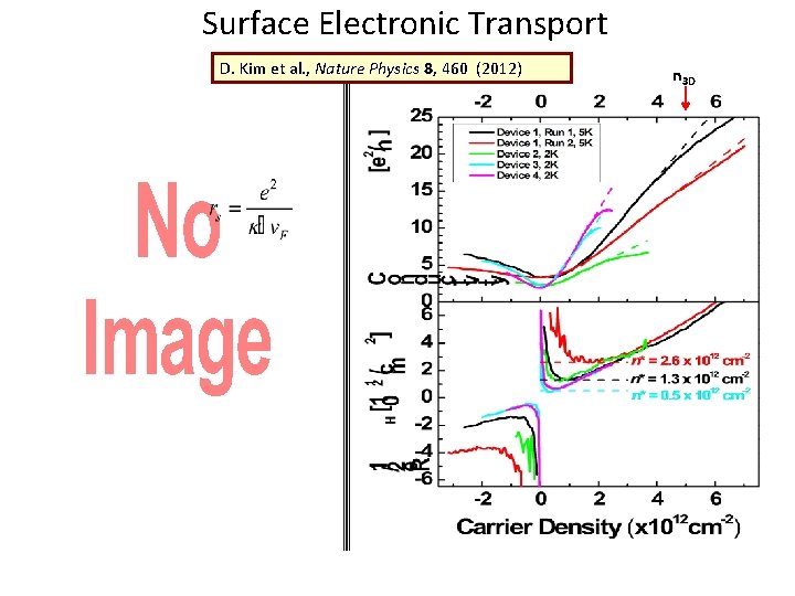
Ambipolar Electric Field Effect D. Kim et al. , Nature Physics 8, 460 (2012) Key Observations Typical n-doping (as fabricated): ~2 x 1013 cm-2 After our schemes applied: ~3 x 1012 cm-2 Clear ambipolar Conduction t ~10 nm n-type e-h p-type Metallic T dependance of ρ As expected for Gapless SS

Surface Electronic Transport D. Kim et al. , Nature Physics 8, 460 (2012) n 3 D

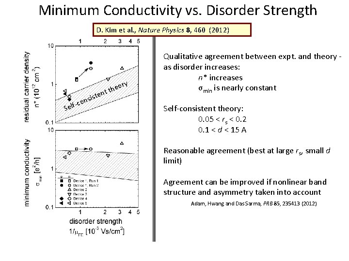
Minimum Conductivity vs. Disorder Strength D. Kim et al. , Nature Physics 8, 460 (2012) Se sis n o c lf- ory te he nt t Qualitative agreement between expt. and theory - as disorder increases: n* increases σmin is nearly constant Self-consistent theory: 0. 05 < rs < 0. 2 0. 1 < d < 15 A Reasonable agreement (best at large rs, small d limit) Agreement can be improved if nonlinear band structure and asymmetry taken into account Adam, Hwang and Das Sarma, PRB 85, 235413 (2012)

Next time: effects of spin and pseudospin K’: k||-x bonding orbitals anti-bonding orbitals K: k||-x K: k||x real-space wavefunctions (color denotes phase) anti-bonding k-space representation K’ bonding K bonding orbitals

Questions?