MetalSemiconductor Contacts 1 Introduction 2 Schottky Contacts 3
- Slides: 23

Metal-Semiconductor Contacts 1. Introduction 2. Schottky Contacts 3. Ohmic Contacts L S Tan - 2011 EE 2004 1

Expected Outcomes At the end of the lectures on metal-semiconductor contacts, you should be able to : • Draw the energy band diagrams of M-S contacts under equilibrium, forward biased and reverse biased conditions. • Predict whether the M-S contacts will be ohmic or rectifying. • Explain the behaviour of the M-S contacts in terms of the movements of the electrons and holes. • Explain how a tunnelling ohmic contact works. L S Tan - 2011 EE 2004 2

Reading q D A Neamen, Semiconductor Physics and Devices, Third Edition, Mc. Graw-Hill (2003), pp. 326 -328, 344 – 347. L S Tan - 2011 EE 2004 3

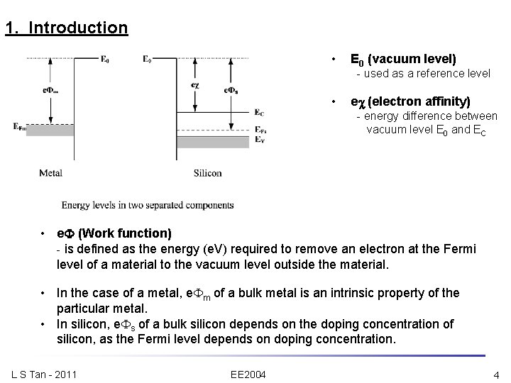
1. Introduction • E 0 (vacuum level) - used as a reference level • e (electron affinity) - energy difference between vacuum level E 0 and EC • e (Work function) - is defined as the energy (e. V) required to remove an electron at the Fermi level of a material to the vacuum level outside the material. • In the case of a metal, e m of a bulk metal is an intrinsic property of the particular metal. • In silicon, e s of a bulk silicon depends on the doping concentration of silicon, as the Fermi level depends on doping concentration. L S Tan - 2011 EE 2004 4

• When a metal and a semiconductor are put into contact with each other, the Fermi level is constant* throughout the metal-semiconductor system at thermal equilibrium. • Unless the work functions of the two materials are equal, this would require the energy bands of one of the materials to move up or down with respect to the other. • However, the vacuum level must be continuous* throughout the system. This would require that the energy bands, E 0, EC and EV, in the semiconductor in the vicinity of the metal-semiconductor interface to bend. • The nature of band bending, which will determine the nature of the contact, will be determined by the difference between e m and e s. * Note : This is the same as the principle applied to p-n junctions. L S Tan - 2011 EE 2004 5

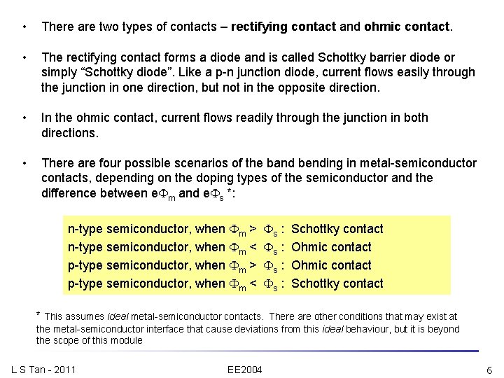
• There are two types of contacts – rectifying contact and ohmic contact. • The rectifying contact forms a diode and is called Schottky barrier diode or simply “Schottky diode”. Like a p-n junction diode, current flows easily through the junction in one direction, but not in the opposite direction. • In the ohmic contact, current flows readily through the junction in both directions. • There are four possible scenarios of the band bending in metal-semiconductor contacts, depending on the doping types of the semiconductor and the difference between e m and e s *: n-type semiconductor, when m > s : Schottky contact n-type semiconductor, when m < s : Ohmic contact p-type semiconductor, when m > s : Ohmic contact p-type semiconductor, when m < s : Schottky contact * This assumes ideal metal-semiconductor contacts. There are other conditions that may exist at the metal-semiconductor interface that cause deviations from this ideal behaviour, but it is beyond the scope of this module L S Tan - 2011 EE 2004 6

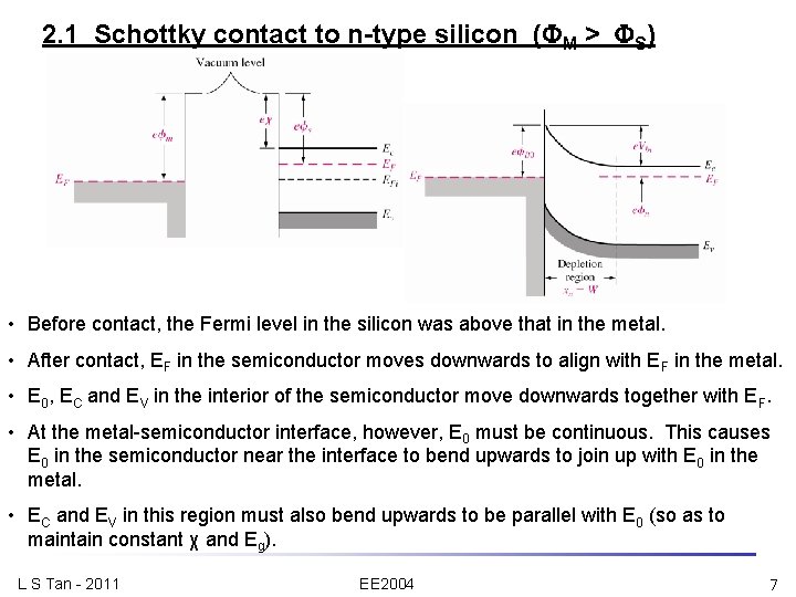
2. 1 Schottky contact to n-type silicon ( M > S) • Before contact, the Fermi level in the silicon was above that in the metal. • After contact, EF in the semiconductor moves downwards to align with EF in the metal. • E 0, EC and EV in the interior of the semiconductor move downwards together with EF. • At the metal-semiconductor interface, however, E 0 must be continuous. This causes E 0 in the semiconductor near the interface to bend upwards to join up with E 0 in the metal. • EC and EV in this region must also bend upwards to be parallel with E 0 (so as to maintain constant χ and Eg). L S Tan - 2011 EE 2004 7

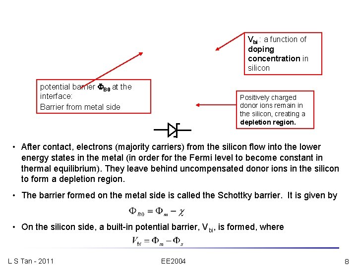
Vbi : a function of doping concentration in silicon potential barrier B 0 at the interface: Barrier from metal side Positively charged donor ions remain in the silicon, creating a depletion region. • After contact, electrons (majority carriers) from the silicon flow into the lower energy states in the metal (in order for the Fermi level to become constant in thermal equilibrium). They leave behind uncompensated donor ions in the silicon to form a depletion region. • The barrier formed on the metal side is called the Schottky barrier. It is given by • On the silicon side, a built-in potential barrier, Vbi, is formed, where L S Tan - 2011 EE 2004 8

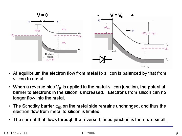
V = 0 e - e e V = VR + e • At equilibrium the electron flow from metal to silicon is balanced by that from silicon to metal. • When a reverse bias VR is applied to the metal-silicon junction, the potential barrier to electrons in the silicon is increased. Electrons from silicon can no longer flow into the metal. • The Schottky barrier B 0 on the metal side remains unchanged, and thus the electron flow from metal to silicon is limited. • The current that flows through the reverse-biased junction is therefore small. L S Tan - 2011 EE 2004 9

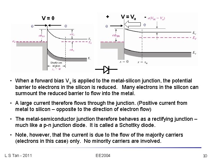
+ V = 0 e e e V = Va e • When a forward bias Va is applied to the metal-silicon junction, the potential barrier to electrons in the silicon is reduced. Many electrons in the silicon can surmount the reduced barrier to flow into the metal. • A large current therefore flows through the junction. (Positive current from metal to silicon – opposite to the direction of electron flow) • The metal-semiconductor junction therefore behaves as a rectifying junction – much like a p-n junction diode. It is called a Schottky diode. • Note, however, that the current is due to the flow of the majority carriers (electrons in this case) only. No minority carriers are involved. L S Tan - 2011 EE 2004 10

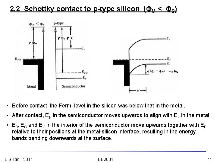
2. 2 Schottky contact to p-type silicon ( M < S) • Before contact, the Fermi level in the silicon was below that in the metal. • After contact, EF in the semiconductor moves upwards to align with EF in the metal. • E 0, EC and EV in the interior of the semiconductor move upwards together with EF, relative to their positions at the metal-silicon interface, resulting in the energy bands bending downwards at the surface. L S Tan - 2011 EE 2004 11

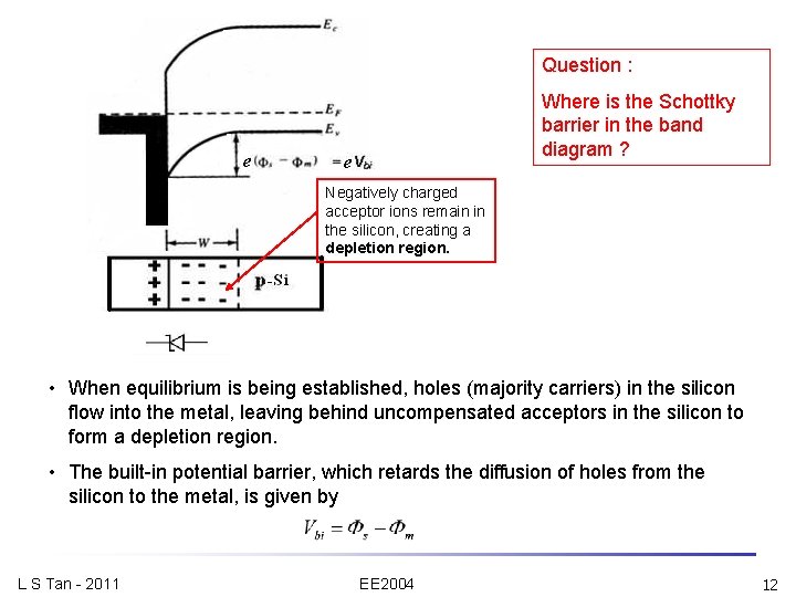
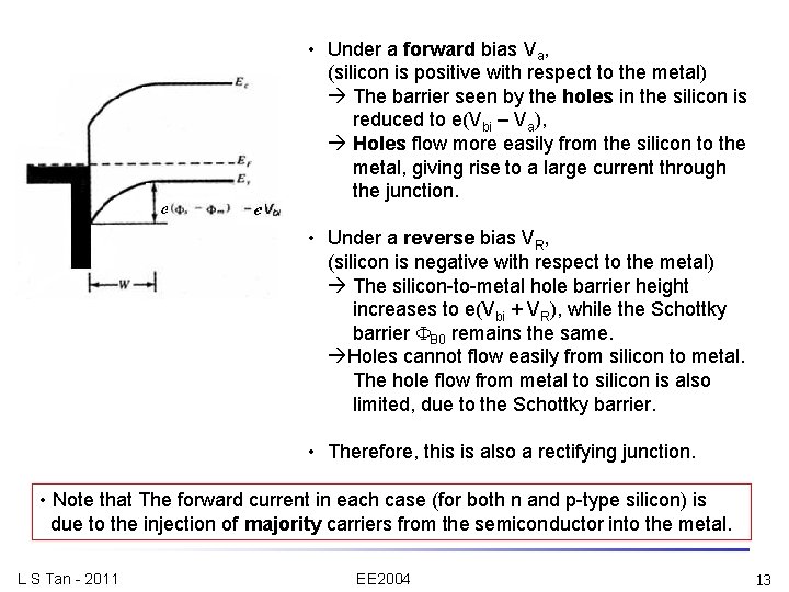
Question : Where is the Schottky barrier in the band diagram ? Negatively charged acceptor ions remain in the silicon, creating a depletion region. • When equilibrium is being established, holes (majority carriers) in the silicon flow into the metal, leaving behind uncompensated acceptors in the silicon to form a depletion region. • The built-in potential barrier, which retards the diffusion of holes from the silicon to the metal, is given by L S Tan - 2011 EE 2004 12

• Under a forward bias Va, (silicon is positive with respect to the metal) The barrier seen by the holes in the silicon is reduced to e(Vbi – Va), Holes flow more easily from the silicon to the metal, giving rise to a large current through the junction. • Under a reverse bias VR, (silicon is negative with respect to the metal) The silicon-to-metal hole barrier height increases to e(Vbi + VR), while the Schottky barrier B 0 remains the same. Holes cannot flow easily from silicon to metal. The hole flow from metal to silicon is also limited, due to the Schottky barrier. • Therefore, this is also a rectifying junction. • Note that The forward current in each case (for both n and p-type silicon) is due to the injection of majority carriers from the semiconductor into the metal. L S Tan - 2011 EE 2004 13

Example 1 An ideal metal-semiconductor contact is formed between gold and n-type silicon, in which the doping Nd = 8 x 1016 cm-3. The work function of gold, eΦm = 5. 1 e. V while the electron affinity of Si, eχ = 4. 01 e. V. Find (a) the metal -semiconductor work function difference, (b) theoretical (ideal) barrier height, ΦB 0, (c) the built-in potential, Vbi, in the semiconductor, (d) the width of the space charge layer, xn, in the semiconductor, when a reverse bias of 3 V is applied. Take T = 300 K, and ni = 1. 5 x 1010 cm-3. L S Tan - 2011 EE 2004 14

Solution to Example 1 L S Tan - 2011 EE 2004 15

Solution to Example 1 (contd) L S Tan - 2011 EE 2004 16

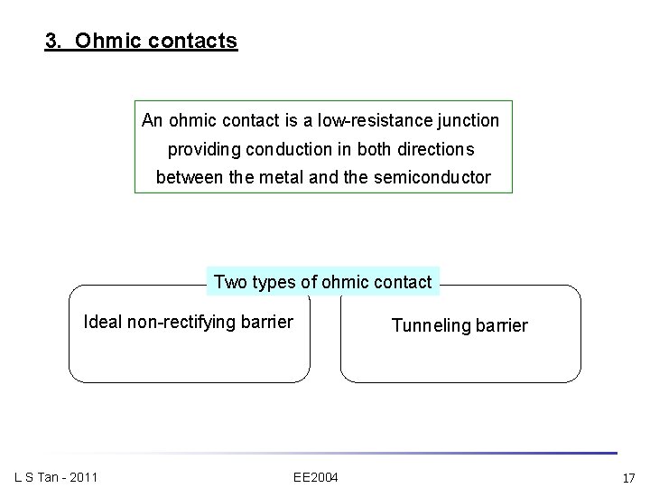
3. Ohmic contacts An ohmic contact is a low-resistance junction providing conduction in both directions between the metal and the semiconductor Two types of ohmic contact Ideal non-rectifying barrier L S Tan - 2011 Tunneling barrier EE 2004 17

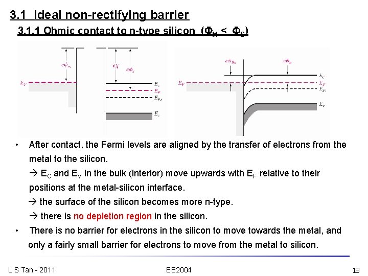
3. 1 Ideal non-rectifying barrier 3. 1. 1 Ohmic contact to n-type silicon ( M < S) • After contact, the Fermi levels are aligned by the transfer of electrons from the metal to the silicon. EC and EV in the bulk (interior) move upwards with EF relative to their positions at the metal-silicon interface. the surface of the silicon becomes more n-type. there is no depletion region in the silicon. • There is no barrier for electrons in the silicon to move towards the metal, and only a fairly small barrier for electrons to move from the metal to silicon. L S Tan - 2011 EE 2004 18

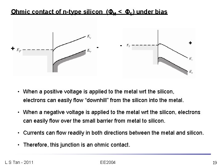
Ohmic contact of n-type silicon ( M < S) under bias - - + + • When a positive voltage is applied to the metal wrt the silicon, electrons can easily flow “downhill” from the silicon into the metal. • When a negative voltage is applied to the metal wrt the silicon, electrons can easily flow over the small barrier from metal to silicon. • Currents can flow readily in both directions between the metal and silicon. • Therefore, this junction is an ohmic contact. L S Tan - 2011 EE 2004 19

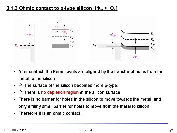
3. 1. 2 Ohmic contact to p-type silicon ( M > S) • After contact, the Fermi levels are aligned by the transfer of holes from the metal to the silicon. • The surface of the silicon becomes more p-type. • There is no depletion region at the silicon surface. • There is no barrier for holes in the silicon to move towards the metal, and only a fairly small barrier for holes to move from the metal to silicon. • Therefore it is an ohmic contact. L S Tan - 2011 EE 2004 20

3. 2 Tunneling barrier • For ideal metal-semiconductor contacts : for n-type semiconductor, when m > s : Schottky contact for n-type semiconductor, when m < s : Ohmic contact for p-type semiconductor, when m > s : Ohmic contact for p-type semiconductor, when m < s : Schottky contact • If a metal forms an ohmic contact with one type of silicon (either n or p), it will form a Schottky contact with the other type. (e. g. , aluminium (Al) forms a good ohmic contact with p-type silicon, but forms a Schottky contact with n-type silicon) • This means, that we need to use two different metals for making ohmic metal contacts to silicon devices (which contain both p- and n-type regions) on a silicon wafer. In practice this is not easy and also increase process complexity. L S Tan - 2011 EE 2004 21

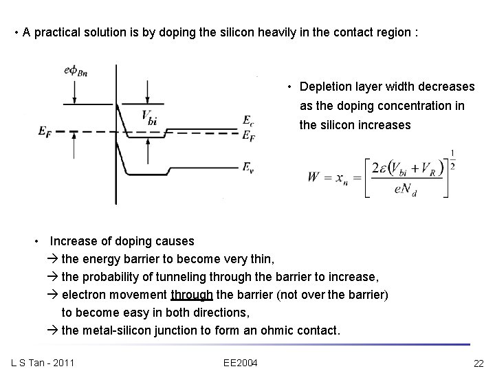
• A practical solution is by doping the silicon heavily in the contact region : • Depletion layer width decreases as the doping concentration in the silicon increases • Increase of doping causes the energy barrier to become very thin, the probability of tunneling through the barrier to increase, electron movement through the barrier (not over the barrier) to become easy in both directions, the metal-silicon junction to form an ohmic contact. L S Tan - 2011 EE 2004 22

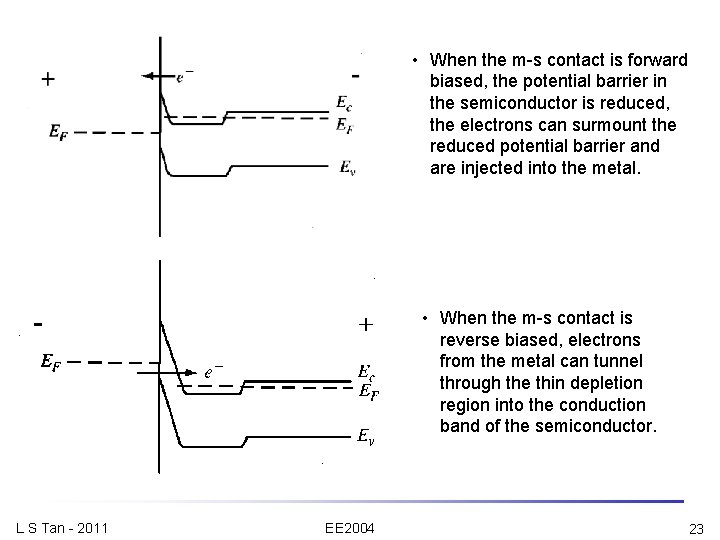
• When the m-s contact is forward biased, the potential barrier in the semiconductor is reduced, the electrons can surmount the reduced potential barrier and are injected into the metal. • When the m-s contact is reverse biased, electrons from the metal can tunnel through the thin depletion region into the conduction band of the semiconductor. L S Tan - 2011 EE 2004 23