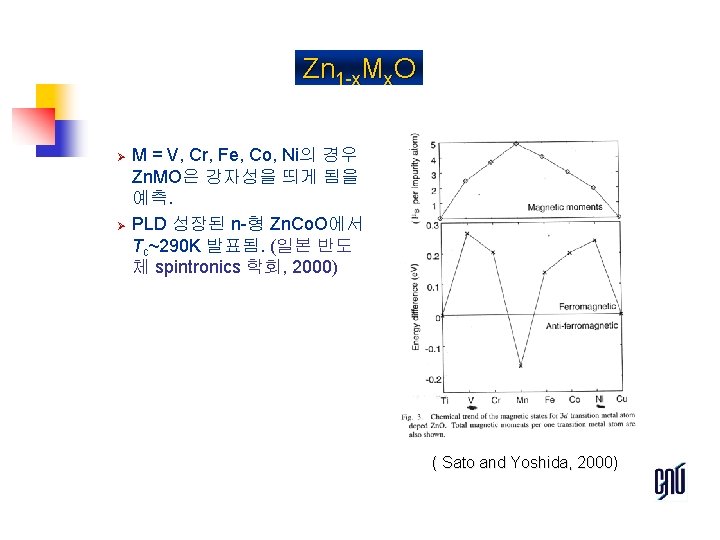
metals band Magnetic transition metals have both s
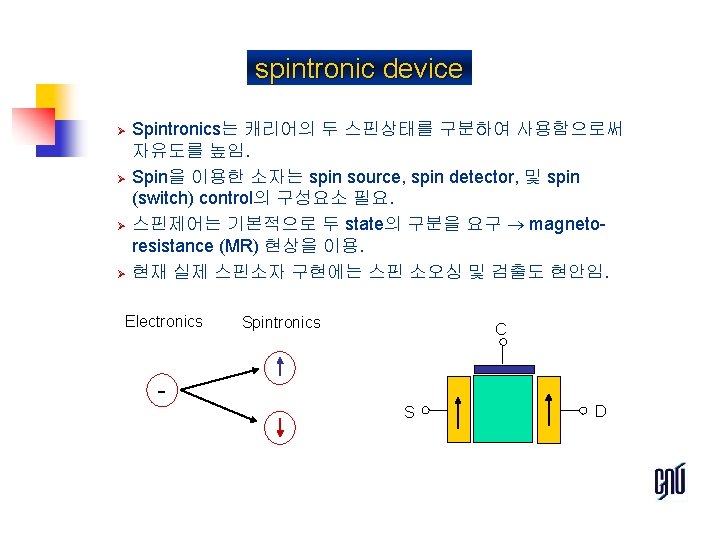

metals band Ø Ø Magnetic transition metals have both s and d states near EF Electrons have higher probability of scattering into the localized d states
를 up-spin과 downspin의 sub-band로 나누어 표시할 수")
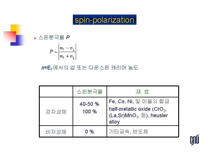
spin-polarization Ø 전도체에서 밴드의 density of states (DOS)를 up-spin과 downspin의 sub-band로 나누어 표시할 수 있음. 1) 비자성체 : symmetric DOS 2) 강자성체 : asymmetric DOS (exchange split). * Half-metallic : 한쪽 스핀방향의 캐리어만 존재. E E EF D non-magnetic(NM) E D ferromagnetic(FM) D half-metallic
이 일어나면서")
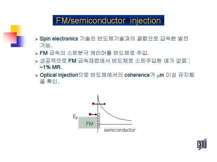
spin coherence/spin relaxation Ø Ø 캐리어는 소재에 injection된 후 이동하면서 스핀산란 (spin scattering)이 일어나면서 스핀특성을 상실 (spin flip). 캐리어가 그 특정 스핀방향을 유지하고 있을 때 coherent하다 하 고, 스핀특성을 잃었을 때 relax되었다고 함. 그 특성거리를 spin coherence (relaxation) length 또는 spin diffusion length, 특성시간 (nano-second 정도)을 spin relaxation (spin-flip, spin decay) time. 스핀분극 캐리어의 큰 확산거리 (소자크기 이상의 spin coherence length) 필요. FM NF spin relaxation
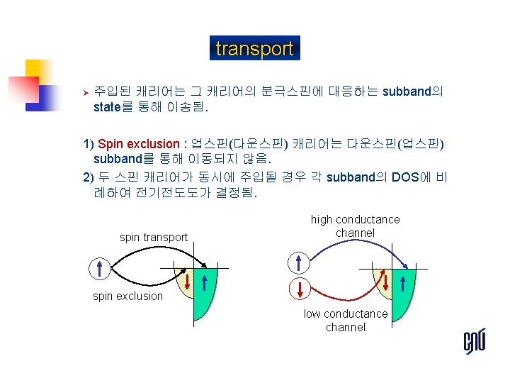

transport q Two current model Ø Ø Assume the spin directions are conserved during scattering Total resistivity comes from a parallel circuit of the two types of carriers (spin-up & spin-down) : major and minor spin bands In ferromagnetic temperature range (T<Tc) For T>Tc, mixing of the spin-up and spin-down channels

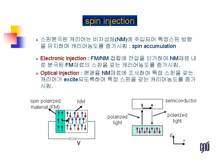
spin injection device Ø Ø GMR의 발견과 이를 이용한 reader head, MRAM 등의 개발로 spin electronics 연구의 활성화. 당면한 문제점은 효율적인 spin injection. § § Ø 고스핀분극 injector 재료 및 구조 고주입효율 (Injector medium 및 medium detector) 재료 및 구조 스핀제어 구조. spin injector spin controller spin detector spin transport medium

FM/metal injection Ø Ø Ø Bipolar spin transistor. All metal, 3 terminal 소자. 서로 다른 coercivity를 갖는 두 FM재료 F 1, F 2와 NM 금속재료 P. F 1 P 스핀주입과 F 1 및 F 2 의 스핀제어에 따른 P-F 2 전압 부호로 신호화. 저저항 다층금속 구조에서 작은 전압 (q. VD<<k. T) 측정의 문제. Spin 확산거리 ~ 1. 5 mm, relaxation time ~ 10 -11 sec in Au. F 1 P F 2 H VD M VD H 1 H 2 H H H 1 H 2 V (Johnson, 1992)

FM/metal injection Ø Ø Ø F 1 P 다운스핀주입으로 P에서 다운스핀 accumulation, 업스핀 depletion (charge neutrality) : P에서의 캐리어 평균에너지는 바 이어스와 상관없이 EFo. F 2의 subband에서 EF는 P의 subband EF와 일치. F 2와 F 1의 스핀이 평행일 때 (+)전압, 반평행일 때 (-)전압. EFo q. VD VD F 2/parallel H H 1 F 1 P q. VD F 2/antiparallel H 2
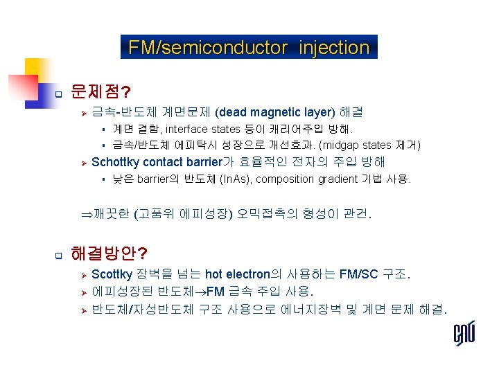
 구조. Injector는 금속+tunnel층, 또는 반도체+space charge영역")
hot-electron injector Ø Ø Ø Spin-valve transistor (emitter-base-collector) 구조. Injector는 금속+tunnel층, 또는 반도체+space charge영역 구조를 사용하여 forward bias 인가로 hot electron 생성 및 injection. Base는 spin valve 구조를 사용하여 자기장에 대해 스핀방향 제 어 기능 및 스핀 selection, filter 기능. Base에 주입된 캐리어 중 collector Scottky장벽을 넘는 스핀캐리 어를 신호로 이용. Figure-of-merit : Magnetocurrent MC(=DIC/ICAP). injector H SV E B SC C VD EF semiconductor V spin valve

tunnel injector Ø Ø P/tunnel barrier/spin valve/SC, FM/tunnel barrier/FM/SC 구조. Spin-valve base 구조에서 MC~400% (77 K) Base폭과 hot elctron의 MFP가 IC 결정 : IC exp(-W/l) 낮은전류 : ~10 -13 A/mm 2 Al 2 O 3 spin-valve base FM tunnel injector (Toshiba/Mizushima et al. , 1997)
. Si/금속 에피성장으로 금속/반도체 계면특성 향상시키고, 두")
SC/FM injector Ø Ø Semiconductor injector (SC/spin-valve/SC 구조). Si/금속 에피성장으로 금속/반도체 계면특성 향상시키고, 두 구조 의 UHV wafer bonding으로 소자구조 제작. 상온에서 MC>200 %. 낮은전류 (~10 -14 A/mm 2). (U. Twente/Monsna et al. , 1997)
와 비자성반도체 접합으로")
magnetic semiconductor Ø Ø Ferromagnetism + semiconducting properties. FM 반도체 (magnetic semiconductor)와 비자성반도체 접합으로 FM/반도체 계면의 문제점 제거. magnetic semiconductor dilute semiconductor nonmagnetic semiconductor (Tohoku U. /Ohno et al. )

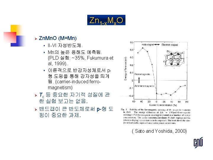
magnetic semiconductor q II-VI dilute magnetic semiconductors Ø Ø q Cd. Te, Zn. Se, etc + Mn Paramagnetic 특성 외부자장 필요. n-형 또는 p-형 도핑 필요하며, 고농도 도핑 어려움 (최근 p-형에 서 강자성 특징 @ T<2 K). 최근 n-형 Be. Mn. Zn. Se (paramagnetic) spin injector 제작. III-V doped magnetic semiconductors Ø Ø Ga. As, In. As, etc + magnetic ion (Mn) Mn은 p-형 도핑효과를 나타내는 동시에 강자성 특성 (halfmetallic) 외부자장 불필요. Mn의 solubility 한계와 이로인한 석출 문제로 주입 제한. 최근 p-형 Mn-doped Ga. As (ferromagnetic) spin injector 제작.
를")
Be. Mn. Zn. Se/Ga. As injection Ø Ø Paramagnetic Be. Mn. Zn. Se (II-VI)를 n-형 도핑하여 spin aligner로 사용 (spin coherence 길이 큼). 주입율 ~90% @2 K, ~3 tesla. Optical detection. 상온 작동 가능성 없음. (U. Würzburg/Fiederling et al. , 1999)
")
Ga. Mn. As/Ga. As injection Ø Ø Ø Ga. Mn. As (x. Mn=4. 5%) + In. Ga. As QW @6 K. 자성반도체/반도체에서 electrical spin injection. Hole coherence length > 200 nm. Optical detectin. 주입율~2%, 스위칭 자기장~40 Oe. (Ohno et al. , 1999)

Ga. Mn. As q MBE growth of Ga. Mn. As Ø Ø 저온 Ga. As MBE (~250 o. C) 성장으로 solubility limit 이상의 (7%) Mn 주입 가능. x. Mn=3. 5~5. 3% : metallic (p ~1020 cm-3) Mn. As formation metallic insulating roughening polycrystalline (Ohno et al. , 1999)

Ga. Mn. As q Magnetism of Ga. Mn. As Ø Ø Ø Hole-induced ferromagnetism. (n-형 In. Mn. As는 강자성특성 없음) Ferromagnetic @ x. Mn>0. 5% Highest Tc~110 K @ x. Mn=5. 3% (Ohno et al. , 1999)
 에서 상온작동")
magnetic semiconductors q Operation temperature of MS Ga. Mn. As (x. Mn>10%) 에서 상온작동 가능. Ø 5% Mn 주입과 p-형 도핑한 III-V 및 II-VI 반도체의 Tc 예측 Ga. Mn. N, Zn. Mn. O의 상온작동 가능성. Ø (Tohoku U. /Dietl et al. , 2000)

magnetic-SC/SC injection Ø Ø 전기적인 스핀검출 소자구조 개발 필요. p-자성반도체/i-반도체/p-자성반도체 구조. Intrinsic 반도체는 다른 밴드갭 반도체 사용하거나 QW tunneling 구조 응용 가능. Collector는 QW 등 고수송효율 구조 채택 가능. electrode pinning layer V pinned magnetic SC semiconductor EF soft semiconductor D electrode substrate D V
- Slides: 28