METALLIZATION Metallization l Metallization is the process that


 Multilayer structure – Shunt")


- Slides: 23
METALLIZATION
Metallization l Metallization is the process that makes accessible the IC to the outside world through conducting pads. l Metallization is one possible step to transfer lithographically defined patterns onto an electronic circuit. l Thin conductive metal films (Al, Cu, Ag etc) are used as interconnects between Si and external leads.
There a large number of different metal deposition techniques. Some major deposition techniques are: l l l Thermal evaporation Sputtering Molecular beam epitaxy (MBE) Chemical vapor deposition (CVD) Deposition by chemical and electrochemical reaction Ion-assisted technique
Desired Properties of Metallization l l l Low resistivity. Easy to form. Easy to etch for pattern generation. Should be stable in oxidizing. Mechanical stability; good adherence, low stress. Surface smoothness. Stability throughout processing, including high temperature sinter, dry or wet oxidation, gettering, phosphorus glass (or any other material) passivation, metallization. No reaction with final metal, aluminum. Should not contaminate devices, wafers, or working apparatus. Good device characteristics and lifetimes. low contact resistance, minimal junction penetration, low electromigration.
Early ICs used pure Al as the interconnect material • Low resistivity • Strong adhesion with Silicon • Corrosion resistant Problems with pure Al • Junction spiking • Electromigration • Stress migration Later ICs used Al alloyed with Cu.
Junction spiking Dissolution of Si take place at only a few points, where spikes are formed One way to minimize spiking is to add Si to the Al by co-evaporation. Another method is to introduce a barrier metal (such as Ti. N) between the Al and Si
Stress migration • Due to difference between coefficient of thermal expansion for Al and Si. • High compressive stresses in Al at high temperatures. • Movement of Al occurs along grain boundaries. • Whole grains of Al pushed upward forming hillocks. • Under tensile stress voids are formed.
Stress migration l l Consequences -Electrical shorts between interconnect levels -Rough surface topography making lithography and etch difficult Solution Addition of elements that have limited solubility. Ex: - Cu atoms segregate and precipitate preferentially along the grain boundaries suppressing hillock formation.
Electromigration • Transfer of electrons in conductor due to flow of current in one direction. • High current densities in the smaller devices are responsible for electron migration. • Metal in some regions pile up and voids form in other regions.
Electromigration l l Alloying with copper (Al with 0. 5%Cu) Multilayer structure – Shunt layer provides alternative path for current flow – If shunt layer has high melting point and strong mechanical properties, they can be more rigid and act as barrier to hillock and void formation.
Thermal stability l At elavated temperatures, metals can react with Si or Si. O 2 to produce unwanted phases. Eg: Silicides. l This limits the maximum processing temperature. l Al on Si < 450 o
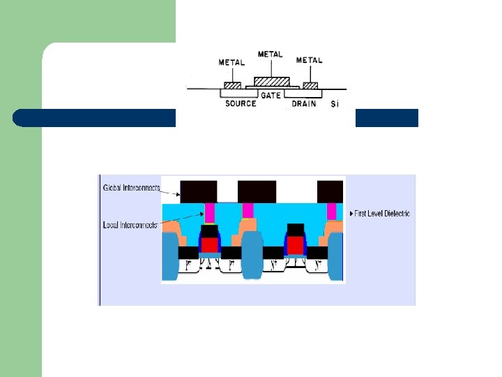
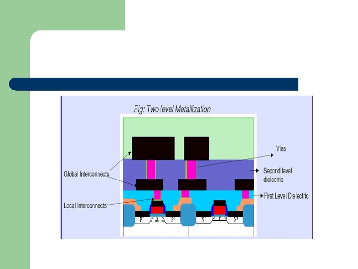
Multilevel metallization l l Three dimensional network of interconnections Metal interconnections • span over several planes • isolated by the insulating dielectric layers. • interconnected by the wiring in the third dimension through the holes in the dielectric planes.
l. Multi level metallization reduces the RC delay
Multilevel metallization l Lower levels: fine connections to individual devices. l Upper levels: thicker/wider common connections.
Adv of Multilevel metallization l l Reduced interconnection lengths Enhanced performance due to reduced RC delay Higher package densities Design flexibility
Future Trends : • Copper has replaced aluminum in upper levels of Metallization. • Damascene patterning/planarization is becoming a key process step in multilevel metallization.
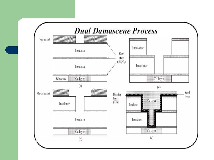
Damascene Technology l Does not require etching. l Make trenches, deposit plating base, then fill with electrodeposition and polish surface. l Mostly, Cu is used. l Metal deposition of Ti. N/Cu (Ti. N serves as a diffusion barrier to prevent Cu from penetrating the dielectric) l Excess Cu on the surface is removed to obtain a planar structure.
Damascene Technology
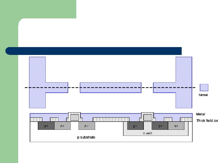
What is the best metal, taking all these factors into account? For Si: l Al-Si-Cu lines (low resistivity) with multilayers of Ti/Ti. N to reduce diffusion and electromigration. l Poly-Si gate contacts (avoids spiking, adequate conductivity) or Silicide/metal gate contacts (e. g. Pt. Si. Ti. Si, made by reacting metal with silicon).