Memory Test Memory organization Memory test complexity Faults
- Slides: 135

Memory Test § § § § Memory organization Memory test complexity Faults and fault models MATS+ march test Address Decoder faults Summary References Copyright 2005 Agrawal & Bushnell Hyderabad, July 27 -29, 2006 (Day 3) 1

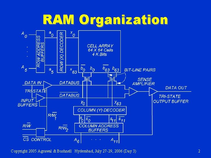
RAM Organization Copyright 2005 Agrawal & Bushnell Hyderabad, July 27 -29, 2006 (Day 3) 2

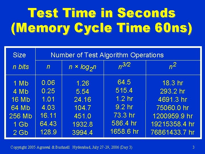
Test Time in Seconds (Memory Cycle Time 60 ns) Size Number of Test Algorithm Operations n bits n n × log 2 n n 3/2 n 2 1 Mb 4 Mb 16 Mb 64 Mb 256 Mb 1 Gb 2 Gb 0. 06 0. 25 1. 01 4. 03 16. 11 64. 43 128. 9 1. 26 5. 54 24. 16 104. 7 451. 0 1932. 8 3994. 4 64. 5 515. 4 1. 2 hr 9. 2 hr 73. 3 hr 586. 4 hr 1658. 6 hr 18. 3 hr 293. 2 hr 4691. 3 hr 75060. 0 hr 1200959. 9 hr 19215358. 4 hr 76861433. 7 hr Copyright 2005 Agrawal & Bushnell Hyderabad, July 27 -29, 2006 (Day 3) 3

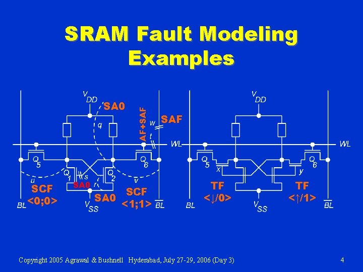
SA 0 SCF <0; 0> SA 0 AF+SAF SRAM Fault Modeling Examples SCF SA 0 <1; 1> SAF TF <↓/0> Copyright 2005 Agrawal & Bushnell Hyderabad, July 27 -29, 2006 (Day 3) TF <↑/1> 4

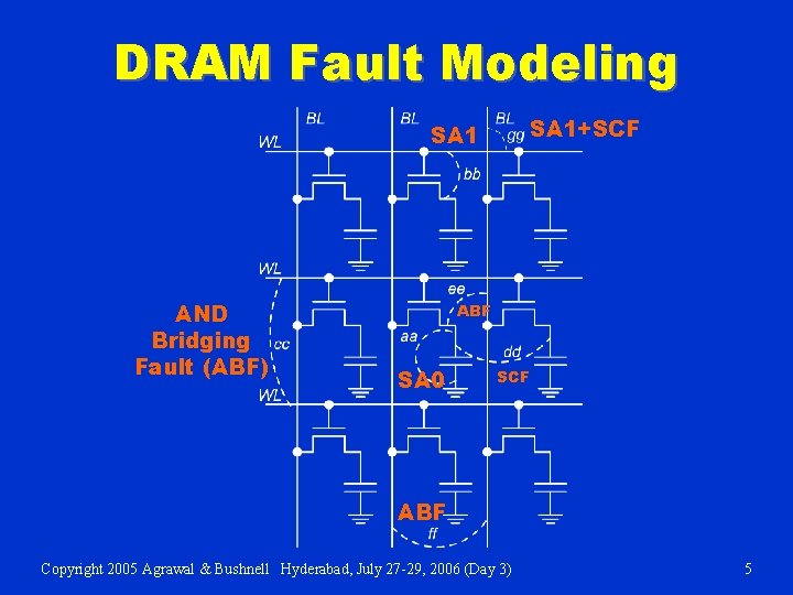
DRAM Fault Modeling SA 1+SCF SA 1 AND Bridging Fault (ABF) ABF SA 0 SCF ABF Copyright 2005 Agrawal & Bushnell Hyderabad, July 27 -29, 2006 (Day 3) 5

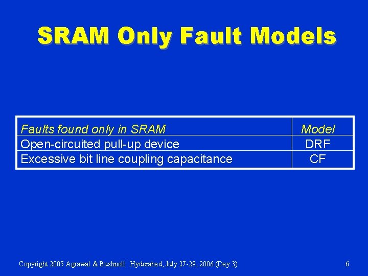
SRAM Only Fault Models Faults found only in SRAM Open-circuited pull-up device Excessive bit line coupling capacitance Copyright 2005 Agrawal & Bushnell Hyderabad, July 27 -29, 2006 (Day 3) Model DRF CF 6

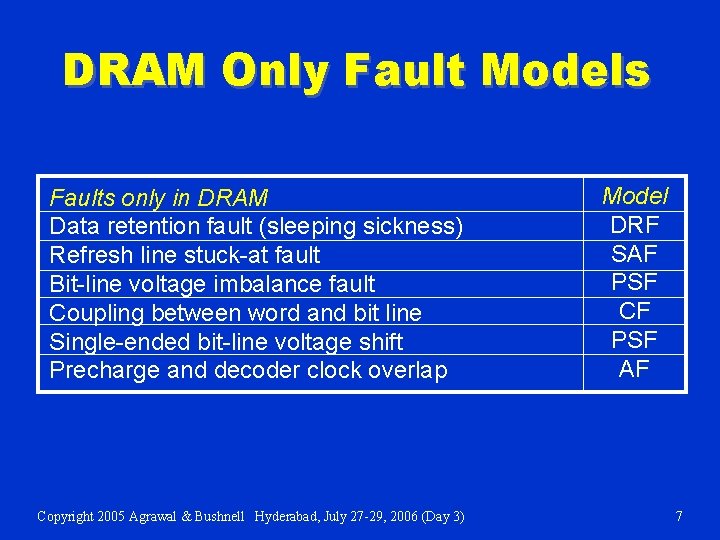
DRAM Only Fault Models Faults only in DRAM Data retention fault (sleeping sickness) Refresh line stuck-at fault Bit-line voltage imbalance fault Coupling between word and bit line Single-ended bit-line voltage shift Precharge and decoder clock overlap Copyright 2005 Agrawal & Bushnell Hyderabad, July 27 -29, 2006 (Day 3) Model DRF SAF PSF CF PSF AF 7

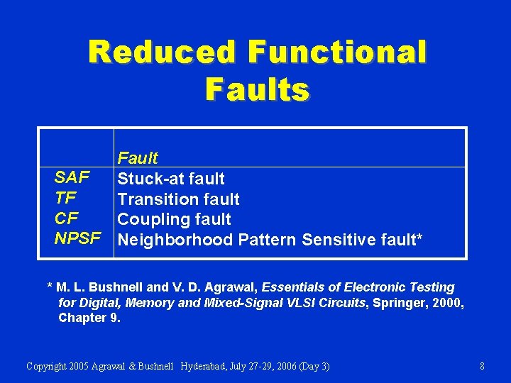
Reduced Functional Faults SAF TF CF NPSF Fault Stuck-at fault Transition fault Coupling fault Neighborhood Pattern Sensitive fault* * M. L. Bushnell and V. D. Agrawal, Essentials of Electronic Testing for Digital, Memory and Mixed-Signal VLSI Circuits, Springer, 2000, Chapter 9. Copyright 2005 Agrawal & Bushnell Hyderabad, July 27 -29, 2006 (Day 3) 8

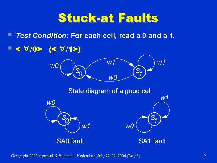
Stuck-at Faults Test Condition: For each cell, read a 0 and a 1. A < /0> (< A § § /1>) Copyright 2005 Agrawal & Bushnell Hyderabad, July 27 -29, 2006 (Day 3) 9

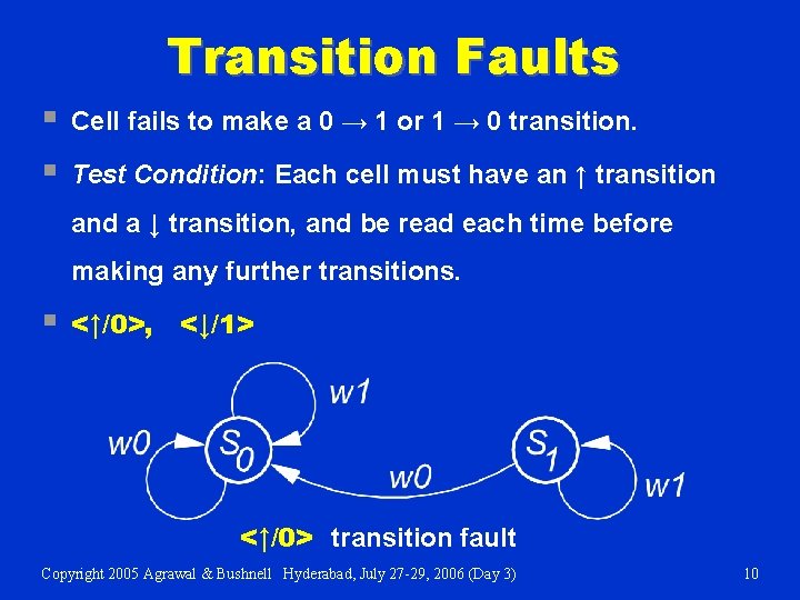
Transition Faults § § Cell fails to make a 0 → 1 or 1 → 0 transition. Test Condition: Each cell must have an ↑ transition and a ↓ transition, and be read each time before making any further transitions. § <↑/0>, <↓/1> <↑/0> transition fault Copyright 2005 Agrawal & Bushnell Hyderabad, July 27 -29, 2006 (Day 3) 10

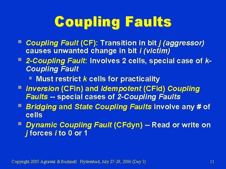
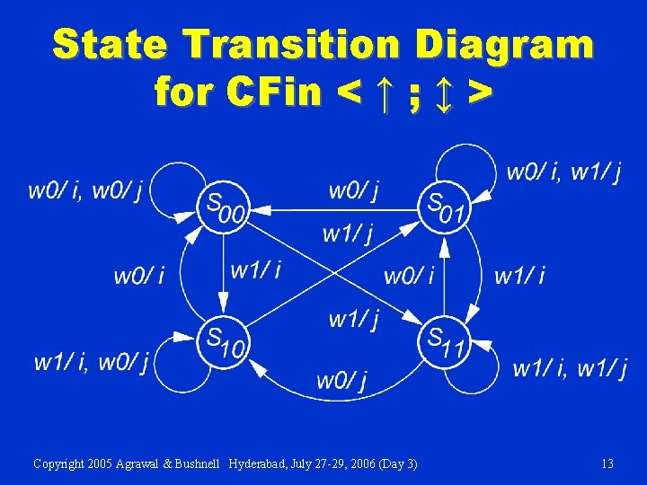
Coupling Faults § § § Coupling Fault (CF): Transition in bit j (aggressor) causes unwanted change in bit i (victim) 2 -Coupling Fault: Involves 2 cells, special case of k. Coupling Fault § Must restrict k cells for practicality Inversion (CFin) and Idempotent (CFid) Coupling Faults -- special cases of 2 -Coupling Faults Bridging and State Coupling Faults involve any # of cells Dynamic Coupling Fault (CFdyn) -- Read or write on j forces i to 0 or 1 Copyright 2005 Agrawal & Bushnell Hyderabad, July 27 -29, 2006 (Day 3) 11

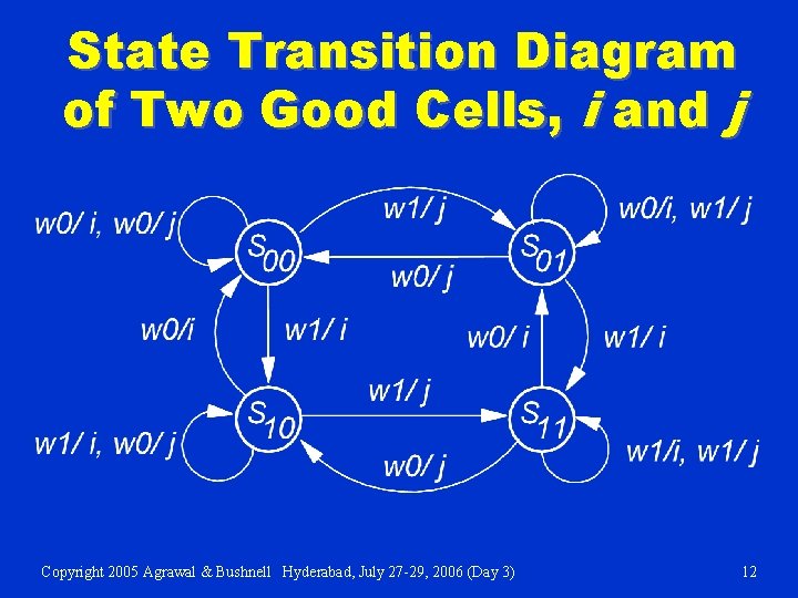
State Transition Diagram of Two Good Cells, i and j Copyright 2005 Agrawal & Bushnell Hyderabad, July 27 -29, 2006 (Day 3) 12

State Transition Diagram for CFin < ↑ ; ↕ > Copyright 2005 Agrawal & Bushnell Hyderabad, July 27 -29, 2006 (Day 3) 13

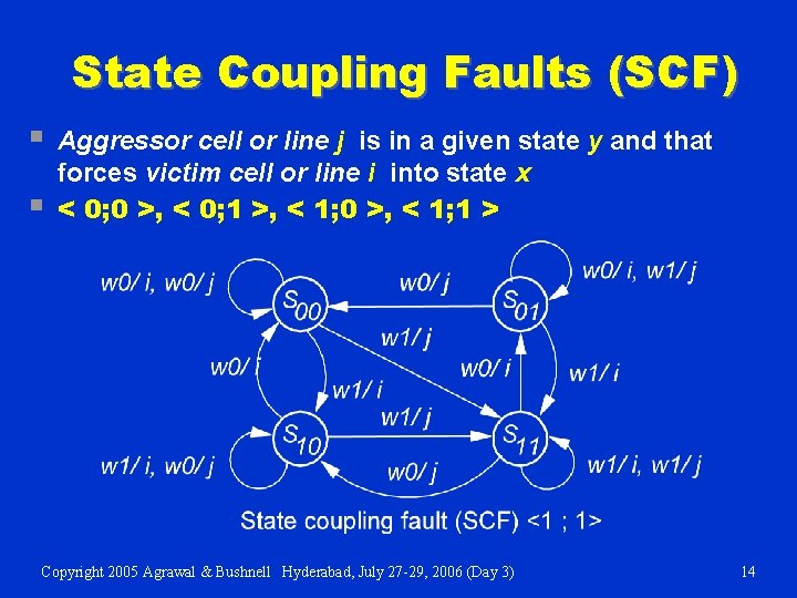
State Coupling Faults (SCF) § § Aggressor cell or line j is in a given state y and that forces victim cell or line i into state x < 0; 0 >, < 0; 1 >, < 1; 0 >, < 1; 1 > Copyright 2005 Agrawal & Bushnell Hyderabad, July 27 -29, 2006 (Day 3) 14

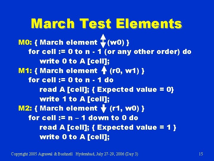
March Test Elements M 0: { March element (w 0) } for cell : = 0 to n - 1 (or any other order) do write 0 to A [cell]; M 1: { March element (r 0, w 1) } for cell : = 0 to n - 1 do read A [cell]; { Expected value = 0} write 1 to A [cell]; M 2: { March element (r 1, w 0) } for cell : = n – 1 down to 0 do read A [cell]; { Expected value = 1 } write 0 to A [cell]; Copyright 2005 Agrawal & Bushnell Hyderabad, July 27 -29, 2006 (Day 3) 15

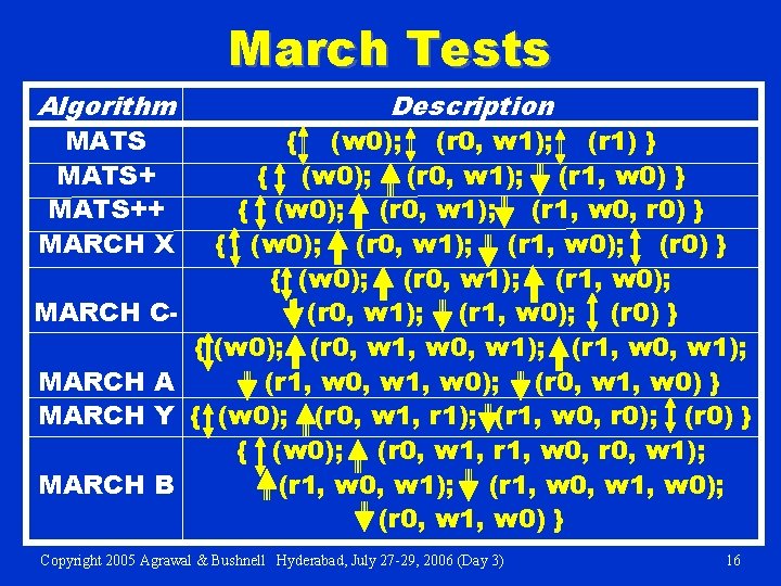
March Tests Algorithm MATS++ MARCH X { Description (w 0); (r 0, w 1); (r 1) } { (w 0); (r 0, w 1); (r 1, w 0, r 0) } { (w 0); (r 0, w 1); (r 1, w 0); (r 0) } { (w 0); (r 0, w 1); (r 1, w 0); MARCH C(r 0, w 1); (r 1, w 0); (r 0) } { (w 0); (r 0, w 1, w 0, w 1); (r 1, w 0, w 1); MARCH A (r 1, w 0, w 1, w 0); (r 0, w 1, w 0) } MARCH Y { (w 0); (r 0, w 1, r 1); (r 1, w 0, r 0); (r 0) } { (w 0); (r 0, w 1, r 1, w 0, r 0, w 1); MARCH B (r 1, w 0, w 1); (r 1, w 0, w 1, w 0); (r 0, w 1, w 0) } Copyright 2005 Agrawal & Bushnell Hyderabad, July 27 -29, 2006 (Day 3) 16

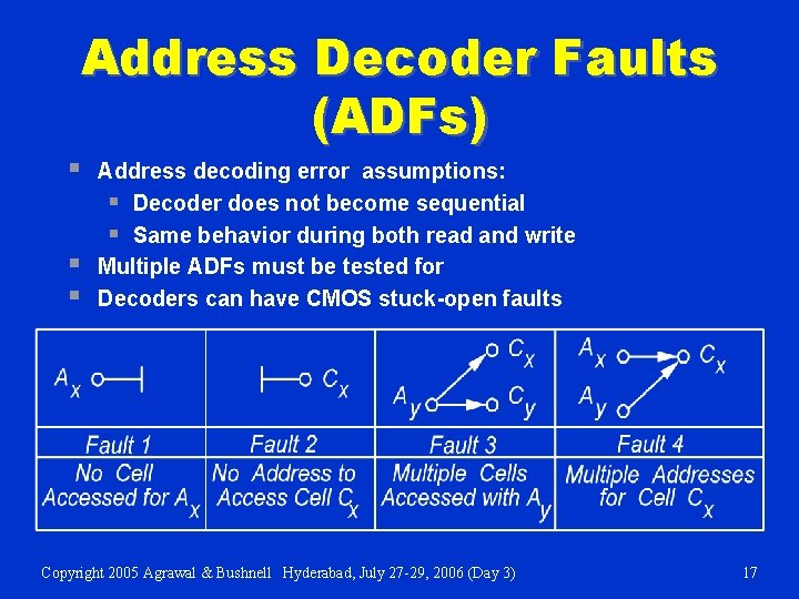
Address Decoder Faults (ADFs) § § § Address decoding error assumptions: § Decoder does not become sequential § Same behavior during both read and write Multiple ADFs must be tested for Decoders can have CMOS stuck-open faults Copyright 2005 Agrawal & Bushnell Hyderabad, July 27 -29, 2006 (Day 3) 17

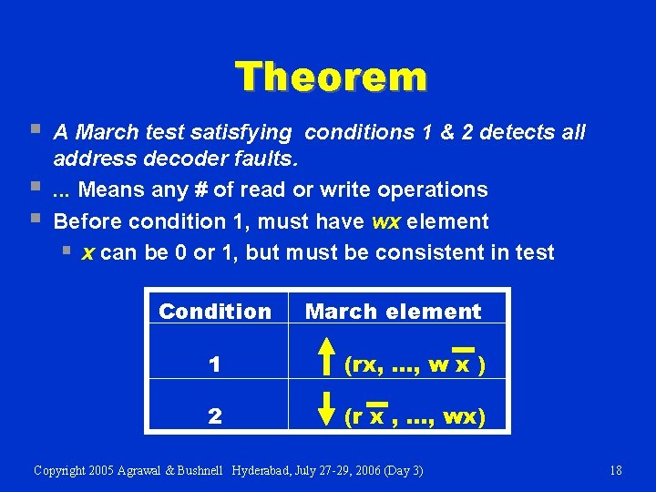
Theorem § § § A March test satisfying conditions 1 & 2 detects all address decoder faults. . Means any # of read or write operations Before condition 1, must have wx element § x can be 0 or 1, but must be consistent in test Condition March element 1 (rx, …, w x ) 2 (r x , …, wx) Copyright 2005 Agrawal & Bushnell Hyderabad, July 27 -29, 2006 (Day 3) 18

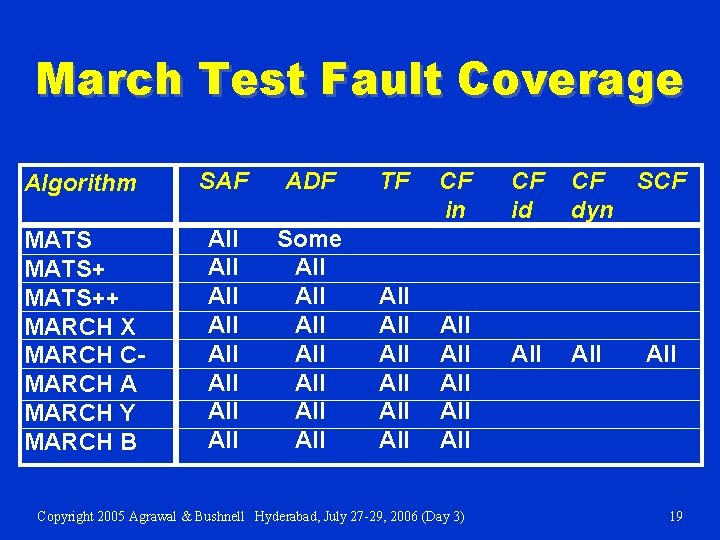
March Test Fault Coverage Algorithm SAF ADF TF MATS++ MARCH X MARCH CMARCH A MARCH Y MARCH B All All Some All All All All CF in All All All Copyright 2005 Agrawal & Bushnell Hyderabad, July 27 -29, 2006 (Day 3) CF id CF SCF dyn All All 19

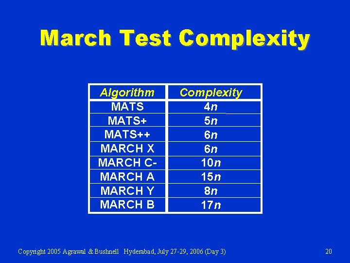
March Test Complexity Algorithm MATS++ MARCH X MARCH CMARCH A MARCH Y MARCH B Complexity 4 n 5 n 6 n 6 n 10 n 15 n 8 n 17 n Copyright 2005 Agrawal & Bushnell Hyderabad, July 27 -29, 2006 (Day 3) 20

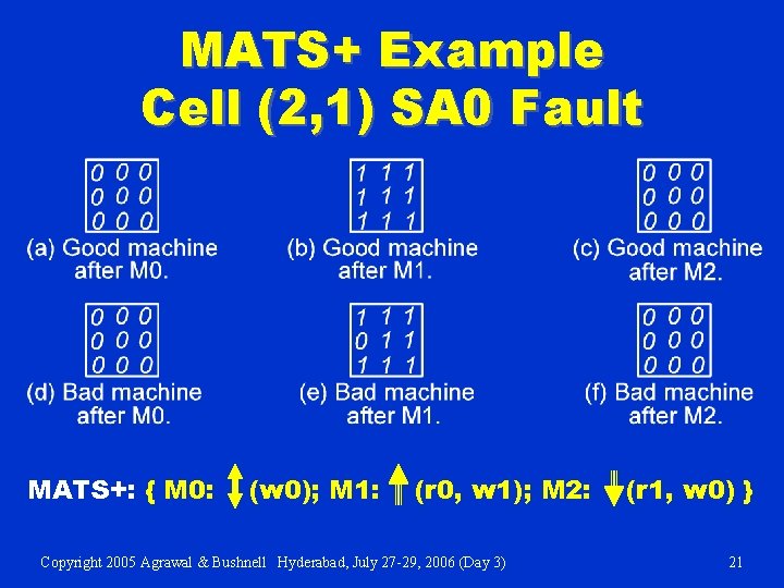
MATS+ Example Cell (2, 1) SA 0 Fault MATS+: { M 0: (w 0); M 1: (r 0, w 1); M 2: Copyright 2005 Agrawal & Bushnell Hyderabad, July 27 -29, 2006 (Day 3) (r 1, w 0) } 21

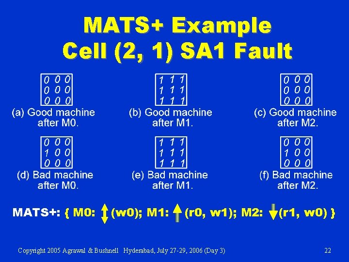
MATS+ Example Cell (2, 1) SA 1 Fault MATS+: { M 0: (w 0); M 1: (r 0, w 1); M 2: Copyright 2005 Agrawal & Bushnell Hyderabad, July 27 -29, 2006 (Day 3) (r 1, w 0) } 22

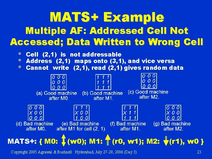
MATS+ Example Multiple AF: Addressed Cell Not Accessed; Data Written to Wrong Cell § § § Cell (2, 1) is not addressable Address (2, 1) maps onto (3, 1), and vice versa Cannot write (2, 1), read (2, 1) gives random data MATS+: { M 0: (w 0); M 1: (r 0, w 1); M 2: Copyright 2005 Agrawal & Bushnell Hyderabad, July 27 -29, 2006 (Day 3) (r 1), w 0 } 23

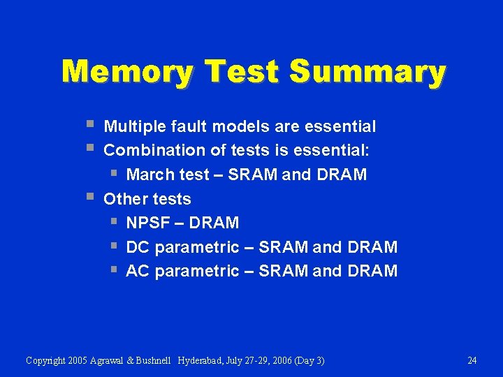
Memory Test Summary § § § Multiple fault models are essential Combination of tests is essential: § March test – SRAM and DRAM Other tests § NPSF – DRAM § DC parametric – SRAM and DRAM § AC parametric – SRAM and DRAM Copyright 2005 Agrawal & Bushnell Hyderabad, July 27 -29, 2006 (Day 3) 24

Memory NPSF and Parametric Test § § § Definitions of NPSFs NPSF test algorithms Parametric tests Summary References Copyright 2005 Agrawal & Bushnell Hyderabad, July 27 -29, 2006 (Day 3) 25

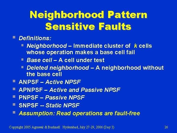
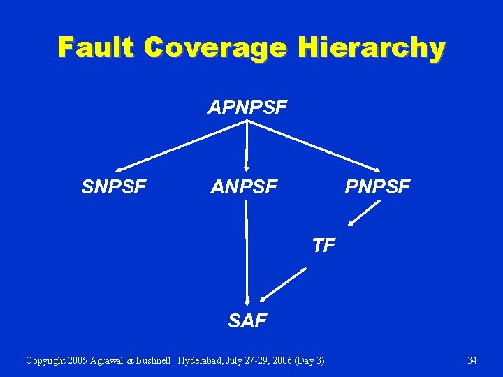
§ § § Neighborhood Pattern Sensitive Faults Definitions: § Neighborhood – Immediate cluster of k cells whose operation makes a base cell fail § Base cell – A cell under test § Deleted neighborhood – A neighborhood without the base cell ANPSF – Active NPSF APNPSF – Active and Passive NPSF PNPSF – Passive NPSF SNPSF -- Static NPSF Assumption: Read operations are fault-free Copyright 2005 Agrawal & Bushnell Hyderabad, July 27 -29, 2006 (Day 3) 26

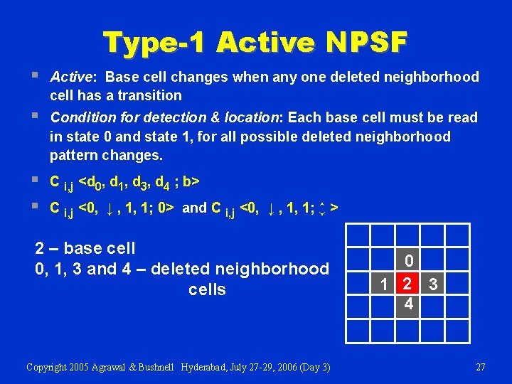
Type-1 Active NPSF § Active: Base cell changes when any one deleted neighborhood cell has a transition § Condition for detection & location: Each base cell must be read in state 0 and state 1, for all possible deleted neighborhood pattern changes. § § C i, j <d 0, d 1, d 3, d 4 ; b> C i, j <0, ↓ , 1, 1; 0> and C i, j <0, ↓ , 1, 1; ↕ > 2 – base cell 0, 1, 3 and 4 – deleted neighborhood cells Copyright 2005 Agrawal & Bushnell Hyderabad, July 27 -29, 2006 (Day 3) 0 1 2 3 4 27

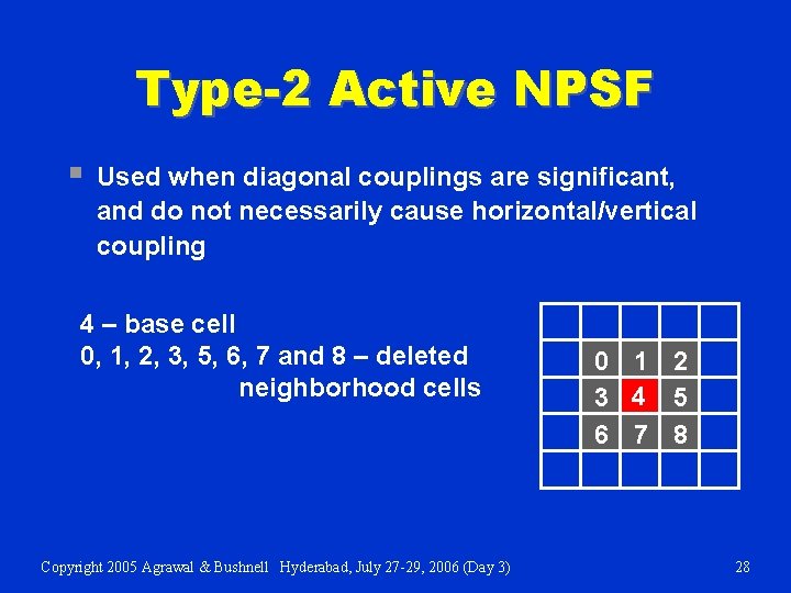
Type-2 Active NPSF § Used when diagonal couplings are significant, and do not necessarily cause horizontal/vertical coupling 4 – base cell 0, 1, 2, 3, 5, 6, 7 and 8 – deleted neighborhood cells Copyright 2005 Agrawal & Bushnell Hyderabad, July 27 -29, 2006 (Day 3) 0 1 2 3 4 5 6 7 8 28

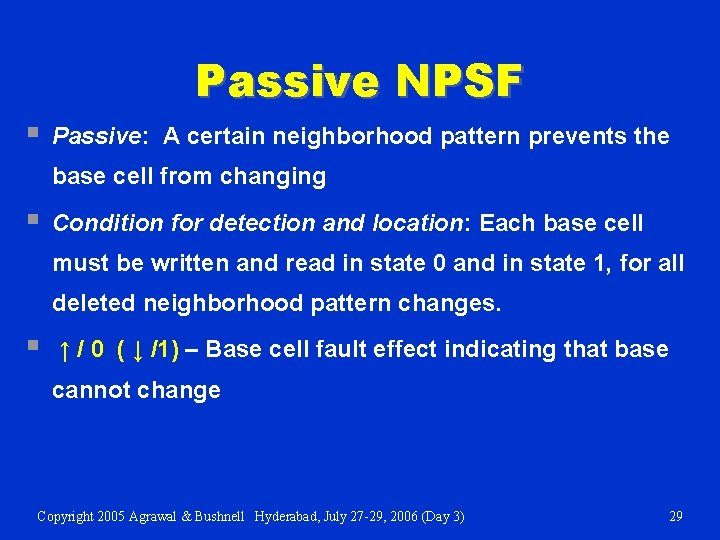
Passive NPSF § Passive: A certain neighborhood pattern prevents the base cell from changing § Condition for detection and location: Each base cell must be written and read in state 0 and in state 1, for all deleted neighborhood pattern changes. § ↑ / 0 ( ↓ /1) – Base cell fault effect indicating that base cannot change Copyright 2005 Agrawal & Bushnell Hyderabad, July 27 -29, 2006 (Day 3) 29

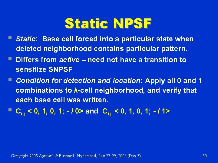
Static NPSF § Static: Base cell forced into a particular state when deleted neighborhood contains particular pattern. § Differs from active – need not have a transition to sensitize SNPSF § Condition for detection and location: Apply all 0 and 1 combinations to k-cell neighborhood, and verify that each base cell was written. § Ci, j < 0, 1, 0, 1; - / 0> and Ci, j < 0, 1, 0, 1; - / 1> Copyright 2005 Agrawal & Bushnell Hyderabad, July 27 -29, 2006 (Day 3) 30

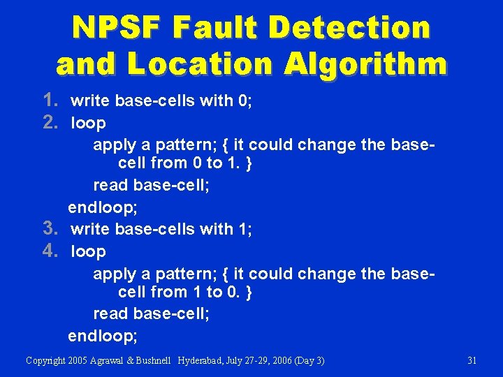
NPSF Fault Detection and Location Algorithm 1. write base-cells with 0; 2. loop apply a pattern; { it could change the basecell from 0 to 1. } read base-cell; endloop; 3. write base-cells with 1; 4. loop apply a pattern; { it could change the basecell from 1 to 0. } read base-cell; endloop; Copyright 2005 Agrawal & Bushnell Hyderabad, July 27 -29, 2006 (Day 3) 31

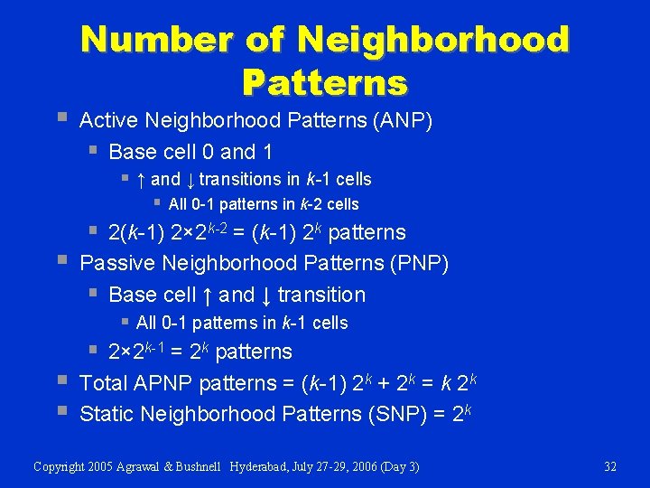
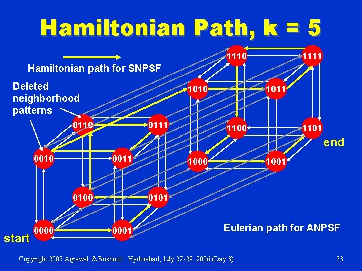
§ Number of Neighborhood Patterns Active Neighborhood Patterns (ANP) § Base cell 0 and 1 § ↑ and ↓ transitions in k-1 cells § All 0 -1 patterns in k-2 cells § § 2(k-1) 2× 2 k-2 = (k-1) 2 k patterns Passive Neighborhood Patterns (PNP) § Base cell ↑ and ↓ transition § All 0 -1 patterns in k-1 cells § 2× 2 k-1 = 2 k patterns Total APNP patterns = (k-1) 2 k + 2 k = k 2 k Static Neighborhood Patterns (SNP) = 2 k Copyright 2005 Agrawal & Bushnell Hyderabad, July 27 -29, 2006 (Day 3) 32

Hamiltonian Path, k = 5 1110 1111 Hamiltonian path for SNPSF Deleted neighborhood patterns 1010 0111 1011 1100 1101 end 0010 0011 0100 start 0000 1001 0101 0001 Eulerian path for ANPSF Copyright 2005 Agrawal & Bushnell Hyderabad, July 27 -29, 2006 (Day 3) 33

Fault Coverage Hierarchy APNPSF SNPSF ANPSF PNPSF TF SAF Copyright 2005 Agrawal & Bushnell Hyderabad, July 27 -29, 2006 (Day 3) 34

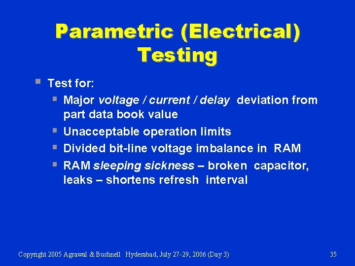
Parametric (Electrical) Testing § Test for: § Major voltage / current / delay deviation from part data book value § Unacceptable operation limits § Divided bit-line voltage imbalance in RAM § RAM sleeping sickness – broken capacitor, leaks – shortens refresh interval Copyright 2005 Agrawal & Bushnell Hyderabad, July 27 -29, 2006 (Day 3) 35

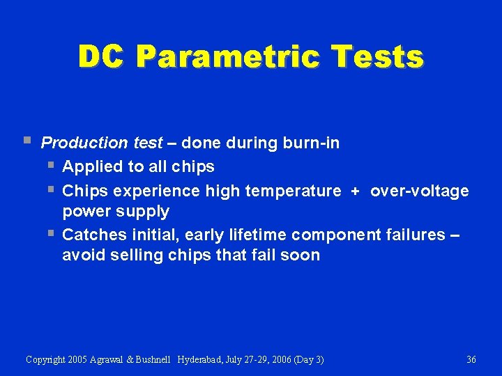
DC Parametric Tests § Production test – done during burn-in § Applied to all chips § Chips experience high temperature + over-voltage power supply § Catches initial, early lifetime component failures – avoid selling chips that fail soon Copyright 2005 Agrawal & Bushnell Hyderabad, July 27 -29, 2006 (Day 3) 36

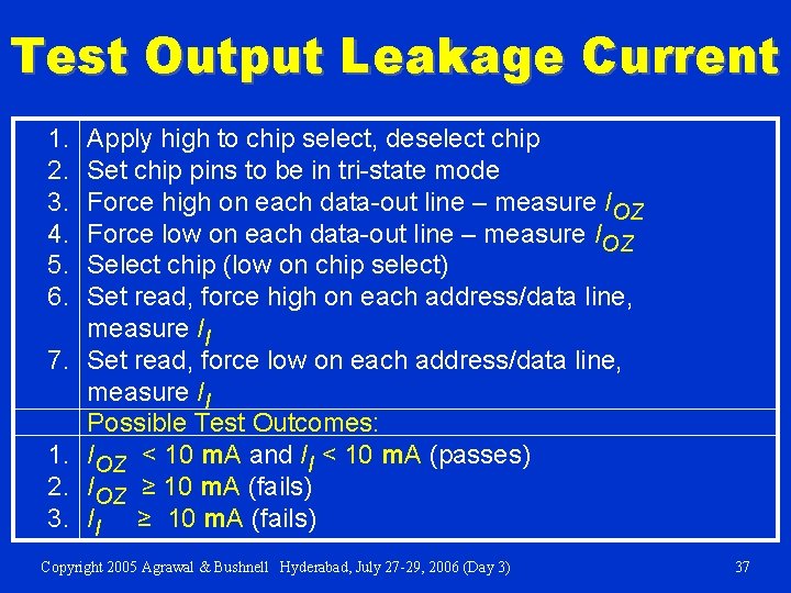
Test Output Leakage Current 1. 2. 3. 4. 5. 6. 7. 1. 2. 3. Apply high to chip select, deselect chip Set chip pins to be in tri-state mode Force high on each data-out line – measure IOZ Force low on each data-out line – measure IOZ Select chip (low on chip select) Set read, force high on each address/data line, measure II Set read, force low on each address/data line, measure II Possible Test Outcomes: IOZ < 10 m. A and II < 10 m. A (passes) IOZ ≥ 10 m. A (fails) II ≥ 10 m. A (fails) Copyright 2005 Agrawal & Bushnell Hyderabad, July 27 -29, 2006 (Day 3) 37

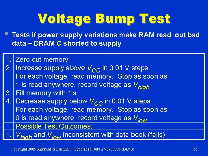
Voltage Bump Test § Tests if power supply variations make RAM read out bad data – DRAM C shorted to supply 1. Zero out memory. 2. Increase supply above VCC in 0. 01 V steps. For each voltage, read memory. Stop as soon as 1 is read anywhere, record voltage as Vhigh 3. Fill memory with 1’s. 4. Decrease supply below VCC in 0. 01 V steps. For each voltage, read memory. Stop as soon as 0 is read anywhere, record voltage as Vlow. Possible Test Outcomes: 1. Vhigh and Vlow inconsistent with data book (fails) Copyright 2005 Agrawal & Bushnell Hyderabad, July 27 -29, 2006 (Day 3) 38

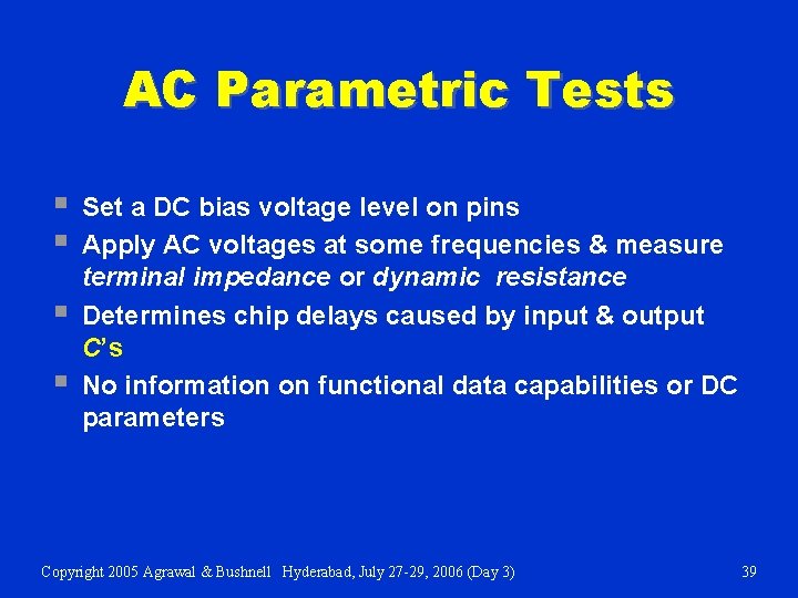
AC Parametric Tests § § Set a DC bias voltage level on pins Apply AC voltages at some frequencies & measure terminal impedance or dynamic resistance Determines chip delays caused by input & output C’s No information on functional data capabilities or DC parameters Copyright 2005 Agrawal & Bushnell Hyderabad, July 27 -29, 2006 (Day 3) 39

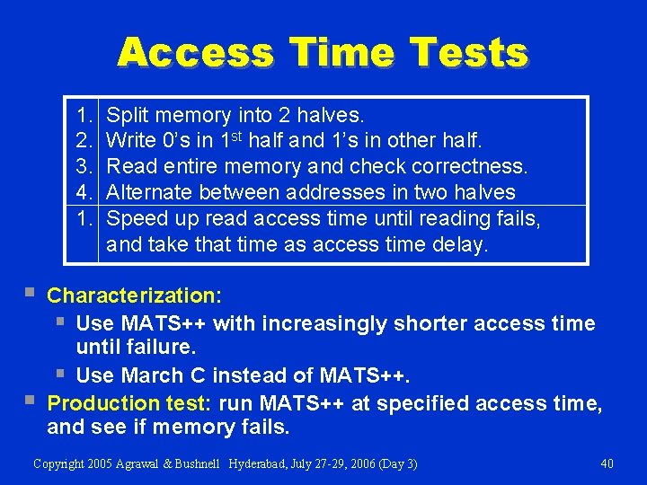
Access Time Tests 1. 2. 3. 4. 1. § § Split memory into 2 halves. Write 0’s in 1 st half and 1’s in other half. Read entire memory and check correctness. Alternate between addresses in two halves Speed up read access time until reading fails, and take that time as access time delay. Characterization: § Use MATS++ with increasingly shorter access time until failure. § Use March C instead of MATS++. Production test: run MATS++ at specified access time, and see if memory fails. Copyright 2005 Agrawal & Bushnell Hyderabad, July 27 -29, 2006 (Day 3) 40

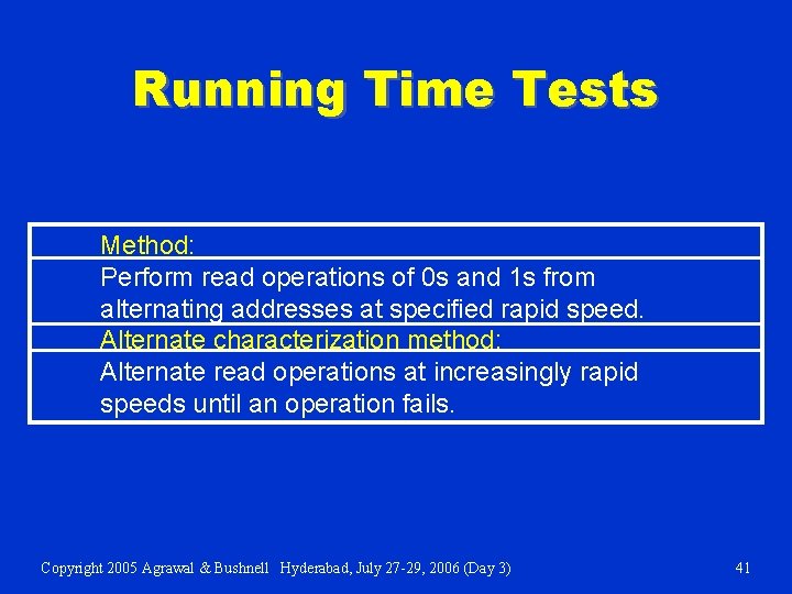
Running Time Tests Method: Perform read operations of 0 s and 1 s from alternating addresses at specified rapid speed. Alternate characterization method: Alternate read operations at increasingly rapid speeds until an operation fails. Copyright 2005 Agrawal & Bushnell Hyderabad, July 27 -29, 2006 (Day 3) 41

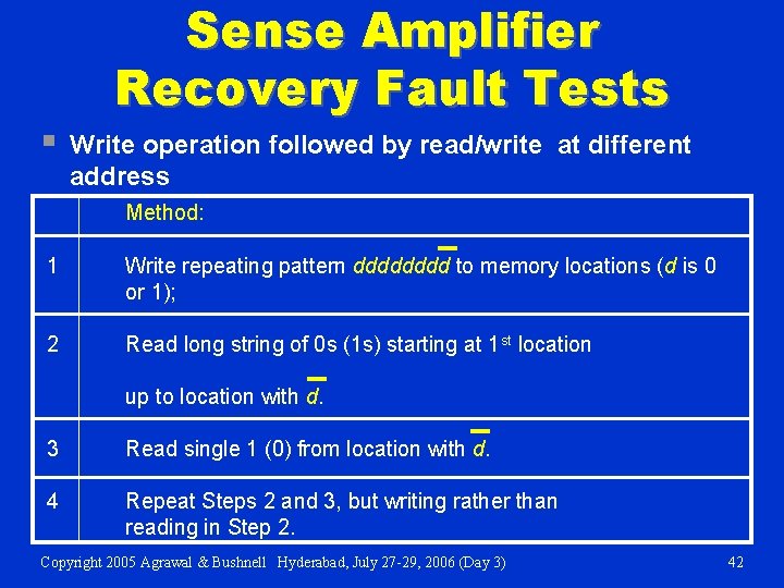
§ Sense Amplifier Recovery Fault Tests Write operation followed by read/write at different address Method: 1 Write repeating pattern dddd to memory locations (d is 0 or 1); 2 Read long string of 0 s (1 s) starting at 1 st location up to location with d. 3 Read single 1 (0) from location with d. 4 Repeat Steps 2 and 3, but writing rather than reading in Step 2. Copyright 2005 Agrawal & Bushnell Hyderabad, July 27 -29, 2006 (Day 3) 42

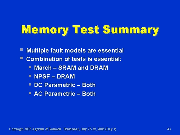
Memory Test Summary § § Multiple fault models are essential Combination of tests is essential: § March – SRAM and DRAM § NPSF – DRAM § DC Parametric – Both § AC Parametric – Both Copyright 2005 Agrawal & Bushnell Hyderabad, July 27 -29, 2006 (Day 3) 43

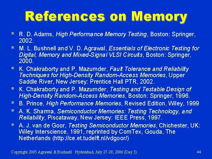
References on Memory § § § § R. D. Adams, High Performance Memory Testing, Boston: Springer, 2002. M. L. Bushnell and V. D. Agrawal, Essentials of Electronic Testing for Digital, Memory and Mixed-Signal VLSI Circuits, Boston: Springer, 2000. K. Chakraborty and P. Mazumder, Fault Tolerance and Reliability Techniques for High-Density Random-Access Memories, Upper Saddle River, New Jersey: Prentice Hall PTR, 2002. K. Chakraborty and P. Mazumder, Testing and Testable Design of High-Density Random-Access Memories, Boston: Springer, 1996. B. Prince, High Performance Memories, Revised Edition, Wiley, 1999 A. K. Sharma, Semiconductor Memories: Testing Technology, and Reliability, Piscataway, New Jersey: IEEE Press, 1997. A. J. van de Goor, Testing Semiconductor Memories, Chichester, UK: Wiley Interscience, 1991, reprinted by Com. Tex, Gouda, The Netherlands (http: //ce. et. tudelft. nl/vdgoor/) Copyright 2005 Agrawal & Bushnell Hyderabad, July 27 -29, 2006 (Day 3) 44

Scan Design for Testability (DFT) Copyright 2005 Agrawal & Bushnell Hyderabad, July 27 -29, 2006 (Day 3) 45

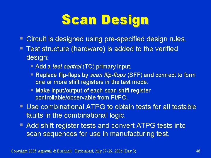
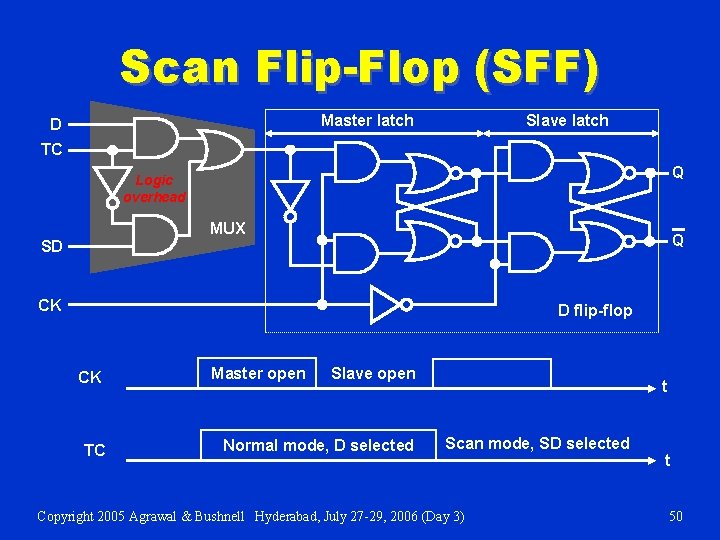
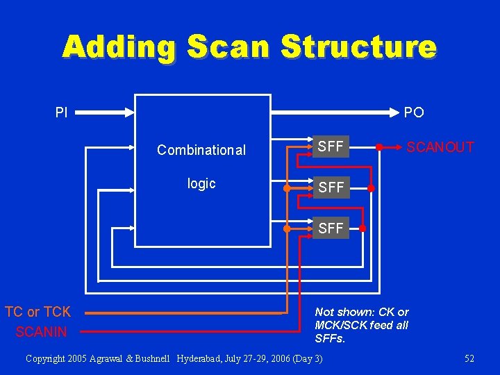
Scan Design § Circuit is designed using pre-specified design rules. § Test structure (hardware) is added to the verified design: § Add a test control (TC) primary input. § Replace flip-flops by scan flip-flops (SFF) and connect to form § one or more shift registers in the test mode. Make input/output of each scan shift register controllable/observable from PI/PO. § Use combinational ATPG to obtain tests for all testable § faults in the combinational logic. Add shift register tests and convert ATPG tests into scan sequences for use in manufacturing test. Copyright 2005 Agrawal & Bushnell Hyderabad, July 27 -29, 2006 (Day 3) 46

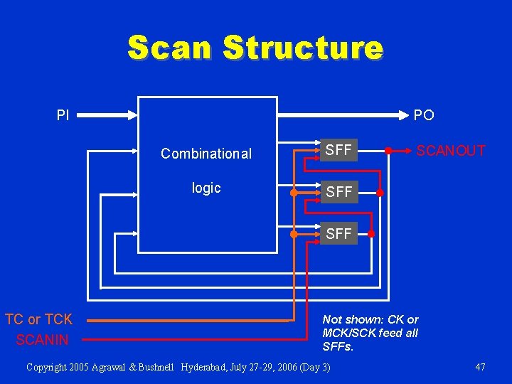
Scan Structure PI PO Combinational SFF logic SFF SCANOUT SFF TC or TCK SCANIN Not shown: CK or MCK/SCK feed all SFFs. Copyright 2005 Agrawal & Bushnell Hyderabad, July 27 -29, 2006 (Day 3) 47

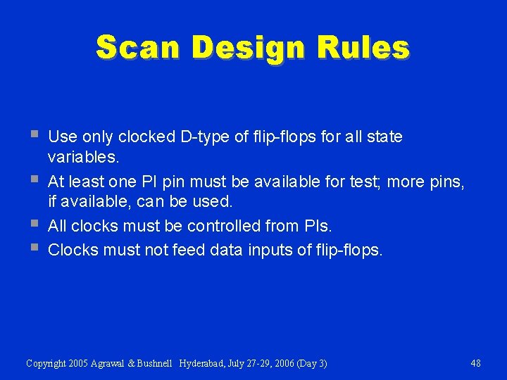
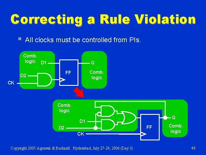
Scan Design Rules § § Use only clocked D-type of flip-flops for all state variables. At least one PI pin must be available for test; more pins, if available, can be used. All clocks must be controlled from PIs. Clocks must not feed data inputs of flip-flops. Copyright 2005 Agrawal & Bushnell Hyderabad, July 27 -29, 2006 (Day 3) 48

Correcting a Rule Violation § All clocks must be controlled from PIs. Comb. logic D 1 Q Comb. logic FF D 2 CK Comb. logic Q D 1 FF D 2 CK Copyright 2005 Agrawal & Bushnell Hyderabad, July 27 -29, 2006 (Day 3) Comb. logic 49

Scan Flip-Flop (SFF) Master latch D Slave latch TC Q Logic overhead MUX Q SD CK D flip-flop CK TC Master open Slave open Normal mode, D selected t Scan mode, SD selected Copyright 2005 Agrawal & Bushnell Hyderabad, July 27 -29, 2006 (Day 3) t 50

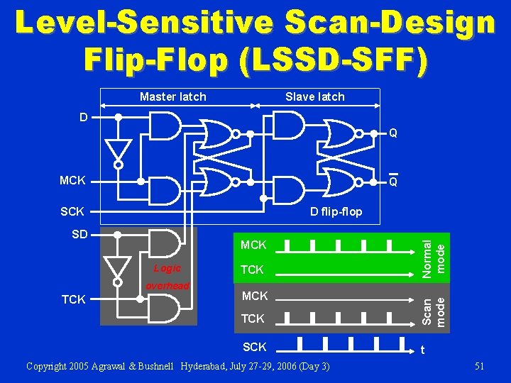
Level-Sensitive Scan-Design Flip-Flop (LSSD-SFF) Master latch Slave latch D Q MCK Q D flip-flop SD MCK overhead TCK MCK TCK Scan mode Logic Normal mode SCK t Copyright 2005 Agrawal & Bushnell Hyderabad, July 27 -29, 2006 (Day 3) 51

Adding Scan Structure PI PO Combinational SFF logic SFF SCANOUT SFF TC or TCK SCANIN Not shown: CK or MCK/SCK feed all SFFs. Copyright 2005 Agrawal & Bushnell Hyderabad, July 27 -29, 2006 (Day 3) 52

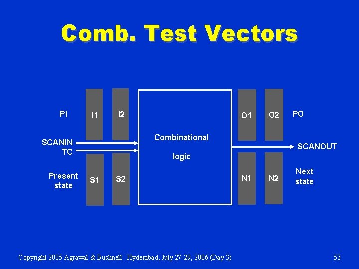
Comb. Test Vectors PI I 1 I 2 O 2 PO Combinational SCANIN TC Present state O 1 SCANOUT logic S 1 S 2 Copyright 2005 Agrawal & Bushnell Hyderabad, July 27 -29, 2006 (Day 3) N 1 N 2 Next state 53

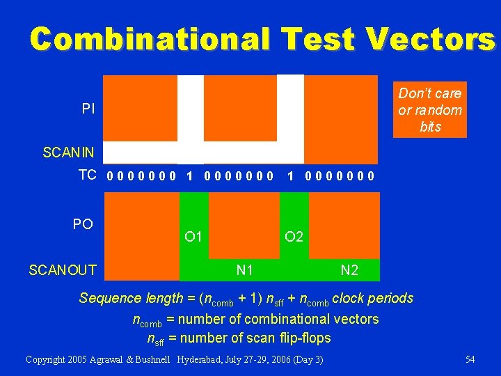
Combinational Test Vectors PI SCANIN I 2 I 1 S 1 Don’t care or random bits S 2 TC 0 0 0 0 1 0 0 0 0 PO SCANOUT O 1 O 2 N 1 N 2 Sequence length = (ncomb + 1) nsff + ncomb clock periods ncomb = number of combinational vectors nsff = number of scan flip-flops Copyright 2005 Agrawal & Bushnell Hyderabad, July 27 -29, 2006 (Day 3) 54

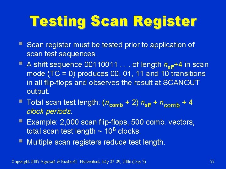
Testing Scan Register § § § Scan register must be tested prior to application of scan test sequences. A shift sequence 0011. . . of length nsff+4 in scan mode (TC = 0) produces 00, 01, 11 and 10 transitions in all flip-flops and observes the result at SCANOUT output. Total scan test length: (ncomb + 2) nsff + ncomb + 4 clock periods. Example: 2, 000 scan flip-flops, 500 comb. vectors, total scan test length ~ 106 clocks. Multiple scan registers reduce test length. Copyright 2005 Agrawal & Bushnell Hyderabad, July 27 -29, 2006 (Day 3) 55

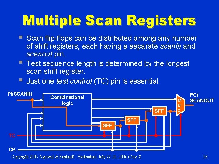
Multiple Scan Registers § § § Scan flip-flops can be distributed among any number of shift registers, each having a separate scanin and scanout pin. Test sequence length is determined by the longest scan shift register. Just one test control (TC) pin is essential. PI/SCANIN Combinational logic SFF M U X PO/ SCANOUT SFF TC CK Copyright 2005 Agrawal & Bushnell Hyderabad, July 27 -29, 2006 (Day 3) 56

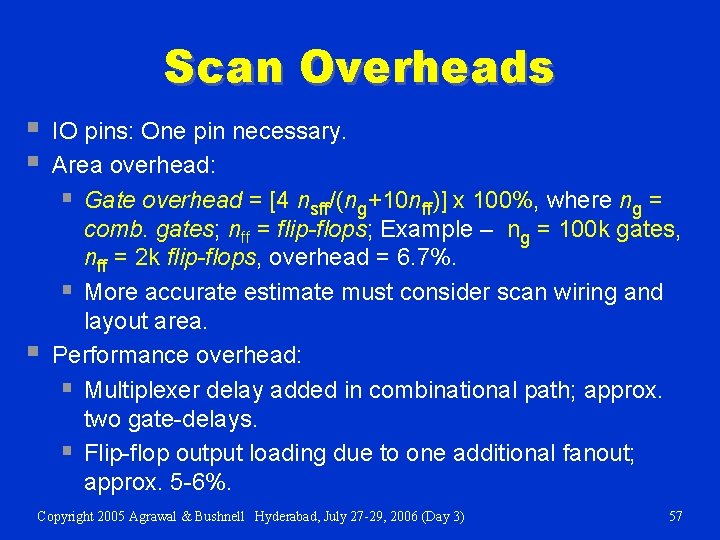
Scan Overheads § § § IO pins: One pin necessary. Area overhead: § Gate overhead = [4 nsff/(ng+10 nff)] x 100%, where ng = comb. gates; nff = flip-flops; Example – ng = 100 k gates, nff = 2 k flip-flops, overhead = 6. 7%. § More accurate estimate must consider scan wiring and layout area. Performance overhead: § Multiplexer delay added in combinational path; approx. two gate-delays. § Flip-flop output loading due to one additional fanout; approx. 5 -6%. Copyright 2005 Agrawal & Bushnell Hyderabad, July 27 -29, 2006 (Day 3) 57

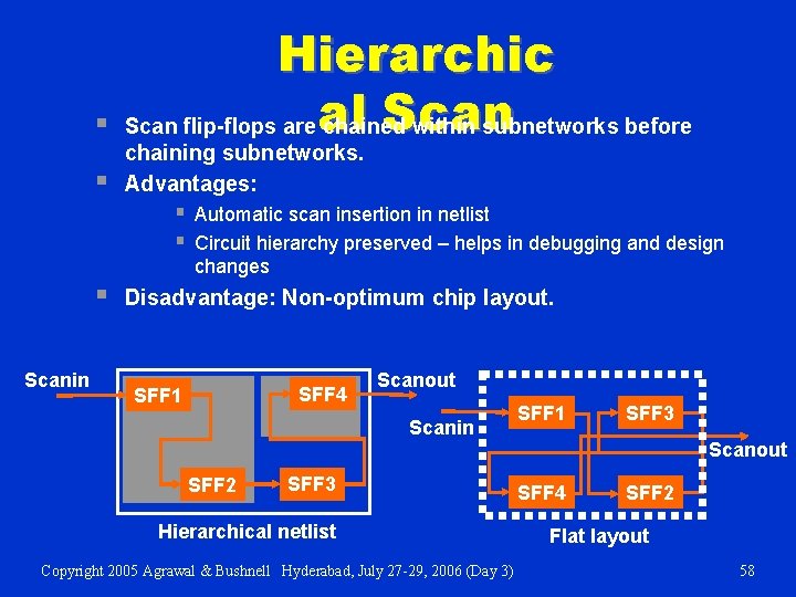
§ § Hierarchic Scan flip-flops are al chained within subnetworks before chaining subnetworks. Advantages: § Automatic scan insertion in netlist § Circuit hierarchy preserved – helps in debugging and design § Scanin changes Disadvantage: Non-optimum chip layout. SFF 4 SFF 1 Scanout Scanin SFF 2 SFF 3 Hierarchical netlist Copyright 2005 Agrawal & Bushnell Hyderabad, July 27 -29, 2006 (Day 3) SFF 1 SFF 3 Scanout SFF 4 SFF 2 Flat layout 58

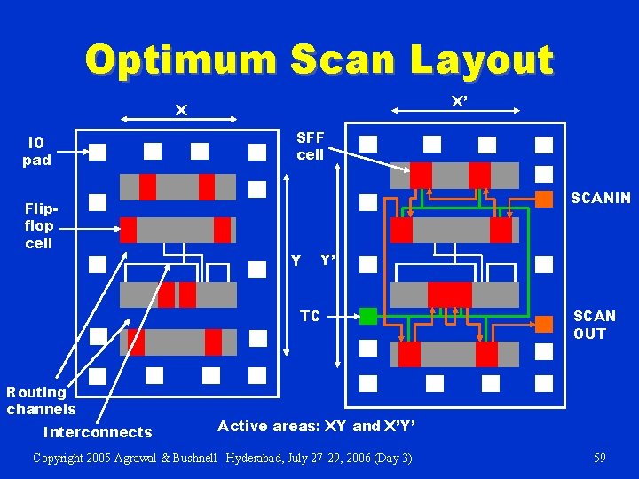
Optimum Scan Layout X’ X IO pad Flipflop cell SFF cell SCANIN Y Y’ TC Routing channels Interconnects SCAN OUT Active areas: XY and X’Y’ Copyright 2005 Agrawal & Bushnell Hyderabad, July 27 -29, 2006 (Day 3) 59

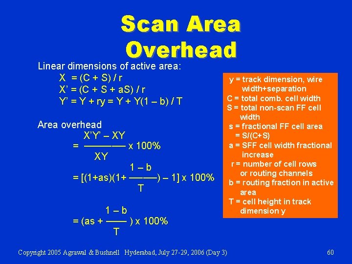
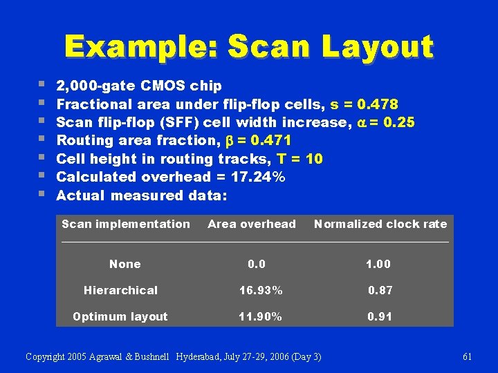
Scan Area Overhead Linear dimensions of active area: X = (C + S) / r X’ = (C + S + a. S) / r Y’ = Y + ry = Y + Y(1 – b) / T Area overhead X’Y’ – XY = ────── x 100% XY 1–b = [(1+as)(1+ ────) – 1] x 100% T 1–b = (as + ─── ) x 100% T y = track dimension, wire width+separation C = total comb. cell width S = total non-scan FF cell width s = fractional FF cell area = S/(C+S) a = SFF cell width fractional increase r = number of cell rows or routing channels b = routing fraction in active area T = cell height in track dimension y Copyright 2005 Agrawal & Bushnell Hyderabad, July 27 -29, 2006 (Day 3) 60

Example: Scan Layout § § § § 2, 000 -gate CMOS chip Fractional area under flip-flop cells, s = 0. 478 Scan flip-flop (SFF) cell width increase, a = 0. 25 Routing area fraction, b = 0. 471 Cell height in routing tracks, T = 10 Calculated overhead = 17. 24% Actual measured data: Scan implementation Area overhead Normalized clock rate ___________________________________ None 0. 0 1. 00 Hierarchical 16. 93% 0. 87 Optimum layout 11. 90% 0. 91 Copyright 2005 Agrawal & Bushnell Hyderabad, July 27 -29, 2006 (Day 3) 61

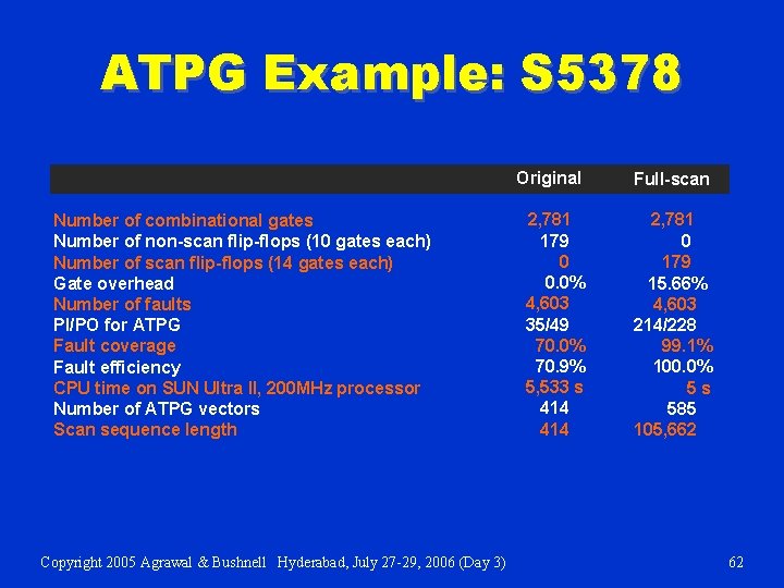
ATPG Example: S 5378 Number of combinational gates Number of non-scan flip-flops (10 gates each) Number of scan flip-flops (14 gates each) Gate overhead Number of faults PI/PO for ATPG Fault coverage Fault efficiency CPU time on SUN Ultra II, 200 MHz processor Number of ATPG vectors Scan sequence length Copyright 2005 Agrawal & Bushnell Hyderabad, July 27 -29, 2006 (Day 3) Original Full-scan 2, 781 179 0 0. 0% 4, 603 35/49 70. 0% 70. 9% 5, 533 s 414 2, 781 0 179 15. 66% 4, 603 214/228 99. 1% 100. 0% 5 s 585 105, 662 62

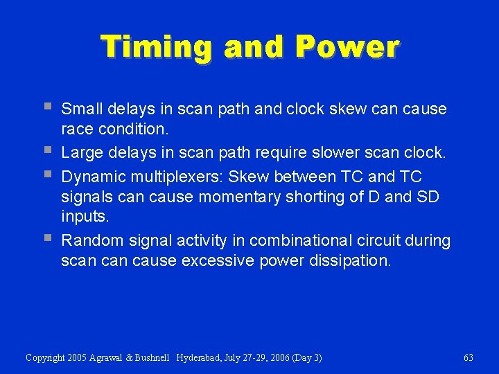
Timing and Power § § Small delays in scan path and clock skew can cause race condition. Large delays in scan path require slower scan clock. Dynamic multiplexers: Skew between TC and TC signals can cause momentary shorting of D and SD inputs. Random signal activity in combinational circuit during scan cause excessive power dissipation. Copyright 2005 Agrawal & Bushnell Hyderabad, July 27 -29, 2006 (Day 3) 63

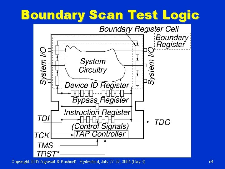
Boundary Scan Test Logic Copyright 2005 Agrawal & Bushnell Hyderabad, July 27 -29, 2006 (Day 3) 64

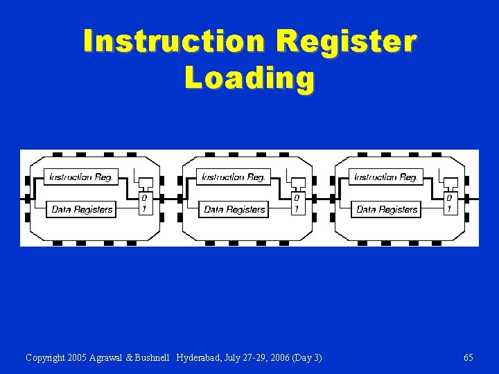
Instruction Register Loading Copyright 2005 Agrawal & Bushnell Hyderabad, July 27 -29, 2006 (Day 3) 65

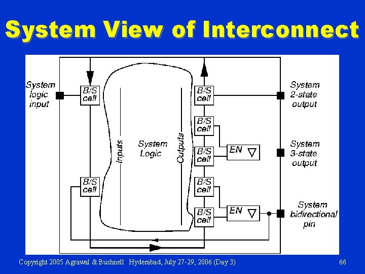
System View of Interconnect Copyright 2005 Agrawal & Bushnell Hyderabad, July 27 -29, 2006 (Day 3) 66

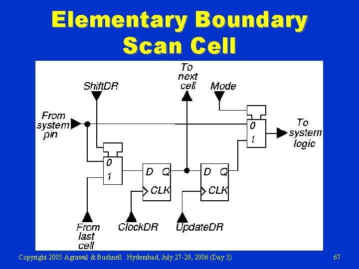
Elementary Boundary Scan Cell Copyright 2005 Agrawal & Bushnell Hyderabad, July 27 -29, 2006 (Day 3) 67

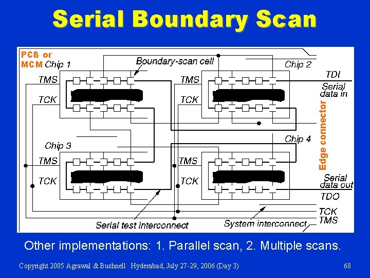
Serial Boundary Scan Edge connector PCB or MCM Other implementations: 1. Parallel scan, 2. Multiple scans. Copyright 2005 Agrawal & Bushnell Hyderabad, July 27 -29, 2006 (Day 3) 68

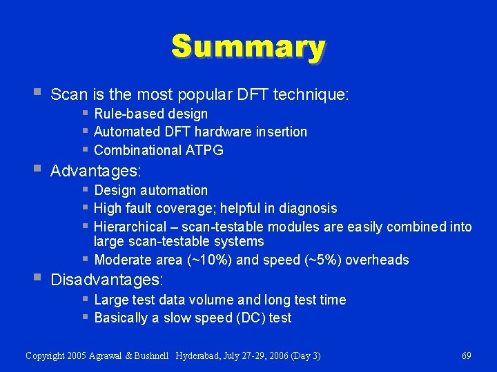
Summary § § § Scan is the most popular DFT technique: § Rule-based design § Automated DFT hardware insertion § Combinational ATPG Advantages: § Design automation § High fault coverage; helpful in diagnosis § Hierarchical – scan-testable modules are easily combined into large scan-testable systems Moderate area (~10%) and speed (~5%) overheads § Disadvantages: § Large test data volume and long test time § Basically a slow speed (DC) test Copyright 2005 Agrawal & Bushnell Hyderabad, July 27 -29, 2006 (Day 3) 69

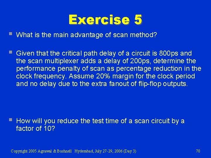
Exercise 5 § What is the main advantage of scan method? § Given that the critical path delay of a circuit is 800 ps and the scan multiplexer adds a delay of 200 ps, determine the performance penalty of scan as percentage reduction in the clock frequency. Assume 20% margin for the clock period and no delay due to the extra fanout of flip-flop outputs. § How will you reduce the test time of a scan circuit by a factor of 10? Copyright 2005 Agrawal & Bushnell Hyderabad, July 27 -29, 2006 (Day 3) 70

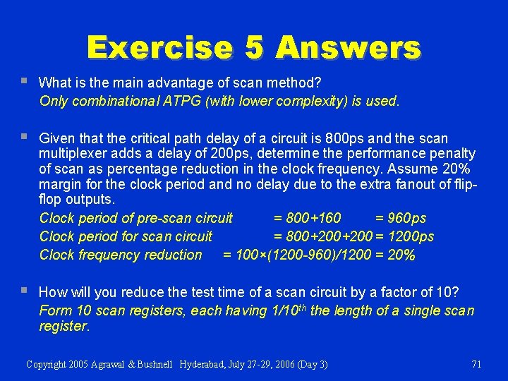
Exercise 5 Answers § What is the main advantage of scan method? Only combinational ATPG (with lower complexity) is used. § Given that the critical path delay of a circuit is 800 ps and the scan multiplexer adds a delay of 200 ps, determine the performance penalty of scan as percentage reduction in the clock frequency. Assume 20% margin for the clock period and no delay due to the extra fanout of flipflop outputs. Clock period of pre-scan circuit = 800+160 = 960 ps Clock period for scan circuit = 800+200 = 1200 ps Clock frequency reduction = 100×(1200 -960)/1200 = 20% § How will you reduce the test time of a scan circuit by a factor of 10? Form 10 scan registers, each having 1/10 th the length of a single scan register. Copyright 2005 Agrawal & Bushnell Hyderabad, July 27 -29, 2006 (Day 3) 71

BIST Built-In Self-Test Copyright 2005 Agrawal & Bushnell Hyderabad, July 27 -29, 2006 (Day 3) 72

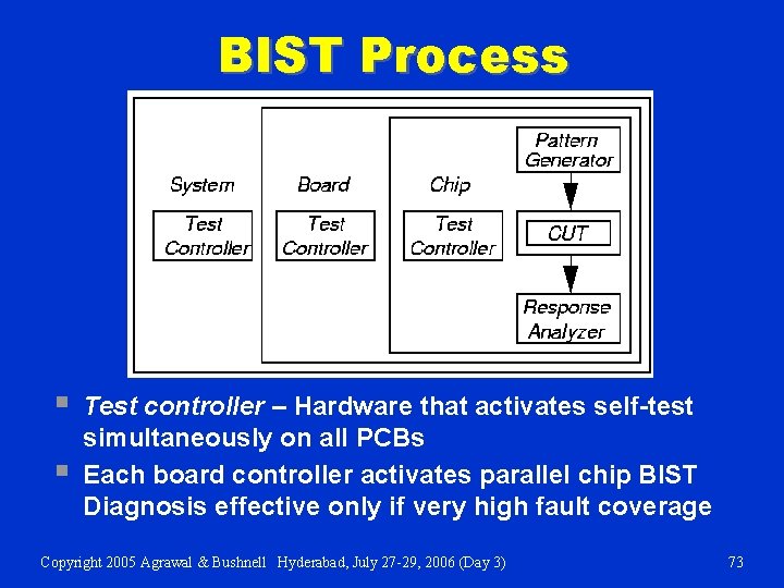
BIST Process § § Test controller – Hardware that activates self-test simultaneously on all PCBs Each board controller activates parallel chip BIST Diagnosis effective only if very high fault coverage Copyright 2005 Agrawal & Bushnell Hyderabad, July 27 -29, 2006 (Day 3) 73

BIST Motivation § § § Useful for field test and diagnosis (less expensive than a local automatic test equipment) Software tests for field test and diagnosis: § Low hardware fault coverage § Low diagnostic resolution § Slow to operate Hardware BIST benefits: § Lower system test effort § Improved system maintenance and repair § Improved component repair § Better diagnosis Copyright 2005 Agrawal & Bushnell Hyderabad, July 27 -29, 2006 (Day 3) 74

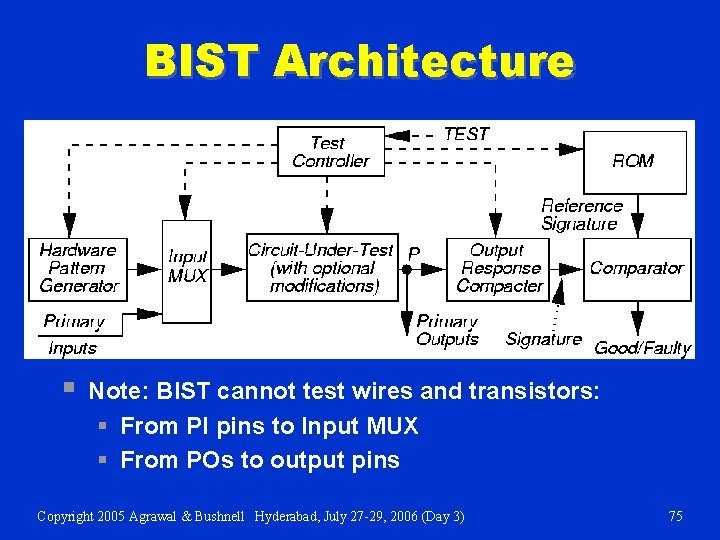
BIST Architecture § Note: BIST cannot test wires and transistors: § From PI pins to Input MUX § From POs to output pins Copyright 2005 Agrawal & Bushnell Hyderabad, July 27 -29, 2006 (Day 3) 75

Pattern Generation § § § § Store in ROM – too expensive Exhaustive Pseudo-exhaustive Pseudo-random (LFSR) – Preferred method Binary counters – use more hardware than LFSR Modified counters Test pattern augmentation § LFSR combined with a few patterns in ROM § Hardware diffracter – generates pattern cluster in neighborhood of pattern stored in ROM Copyright 2005 Agrawal & Bushnell Hyderabad, July 27 -29, 2006 (Day 3) 76

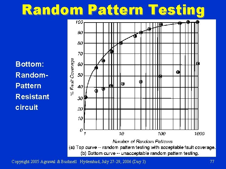
Random Pattern Testing Bottom: Random. Pattern Resistant circuit Copyright 2005 Agrawal & Bushnell Hyderabad, July 27 -29, 2006 (Day 3) 77

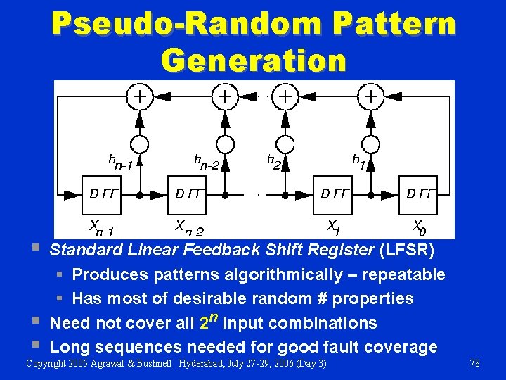
Pseudo-Random Pattern Generation § § § Standard Linear Feedback Shift Register (LFSR) § Produces patterns algorithmically – repeatable § Has most of desirable random # properties Need not cover all 2 n input combinations Long sequences needed for good fault coverage Copyright 2005 Agrawal & Bushnell Hyderabad, July 27 -29, 2006 (Day 3) 78

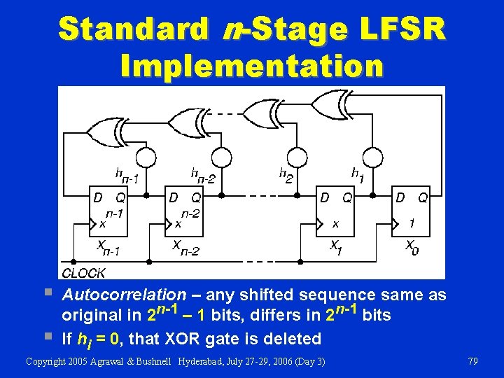
Standard n-Stage LFSR Implementation § § Autocorrelation – any shifted sequence same as original in 2 n-1 – 1 bits, differs in 2 n-1 bits If hi = 0, that XOR gate is deleted Copyright 2005 Agrawal & Bushnell Hyderabad, July 27 -29, 2006 (Day 3) 79

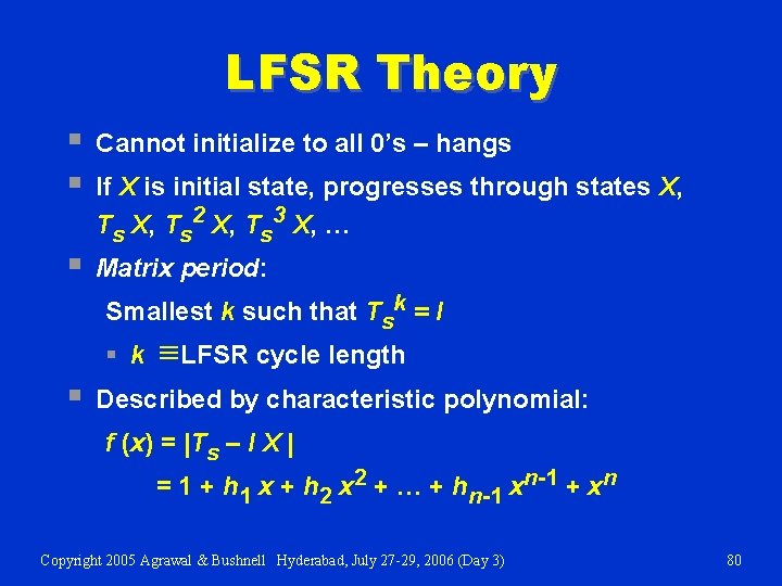
LFSR Theory § § Cannot initialize to all 0’s – hangs § Matrix period: If X is initial state, progresses through states X, Ts 2 X, Ts 3 X, … Smallest k such that Tsk = I § k § º LFSR cycle length Described by characteristic polynomial: f (x) = |Ts – I X | = 1 + h 1 x + h 2 x 2 + … + hn-1 xn-1 + xn Copyright 2005 Agrawal & Bushnell Hyderabad, July 27 -29, 2006 (Day 3) 80

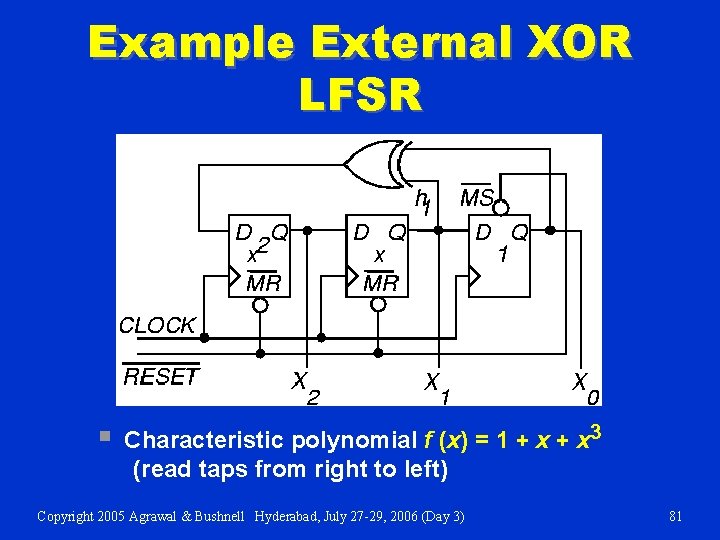
Example External XOR LFSR § Characteristic polynomial f (x) = 1 + x 3 (read taps from right to left) Copyright 2005 Agrawal & Bushnell Hyderabad, July 27 -29, 2006 (Day 3) 81

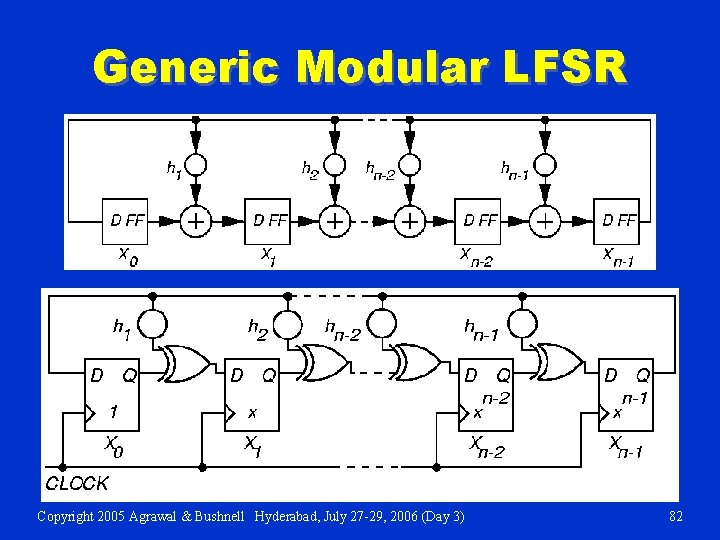
Generic Modular LFSR Copyright 2005 Agrawal & Bushnell Hyderabad, July 27 -29, 2006 (Day 3) 82

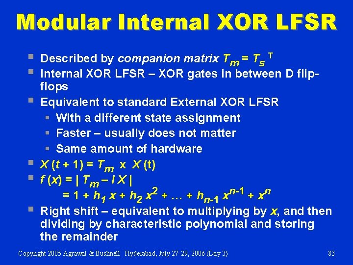
Modular Internal XOR LFSR § § § Described by companion matrix Tm = Ts T Internal XOR LFSR – XOR gates in between D flipflops Equivalent to standard External XOR LFSR § With a different state assignment § Faster – usually does not matter § Same amount of hardware X (t + 1) = Tm x X (t) f (x) = | Tm – I X | = 1 + h 1 x + h 2 x 2 + … + hn-1 xn-1 + xn Right shift – equivalent to multiplying by x, and then dividing by characteristic polynomial and storing the remainder Copyright 2005 Agrawal & Bushnell Hyderabad, July 27 -29, 2006 (Day 3) 83

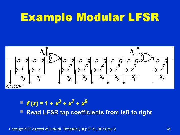
Example Modular LFSR § § f (x) = 1 + x 2 + x 7 + x 8 Read LFSR tap coefficients from left to right Copyright 2005 Agrawal & Bushnell Hyderabad, July 27 -29, 2006 (Day 3) 84

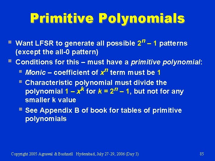
Primitive Polynomials § § Want LFSR to generate all possible 2 n – 1 patterns (except the all-0 pattern) Conditions for this – must have a primitive polynomial: § Monic – coefficient of xn term must be 1 § Characteristic polynomial must divide the polynomial 1 – xk for k = 2 n – 1, but not for any smaller k value § See Appendix B of book for tables of primitive polynomials Copyright 2005 Agrawal & Bushnell Hyderabad, July 27 -29, 2006 (Day 3) 85

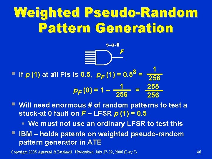
Weighted Pseudo-Random Pattern Generation s-a-0 F § § § 1 256 1 p. F (0) = 1 – = 255 256 Will need enormous # of random patterns to test a stuck-at 0 fault on F – LFSR p (1) = 0. 5 § We must not use an ordinary LFSR to test this IBM – holds patents on weighted pseudo-random pattern generator in ATE If p (1) at all f PIs is 0. 5, p. F (1) = 0. 58 = Copyright 2005 Agrawal & Bushnell Hyderabad, July 27 -29, 2006 (Day 3) 86

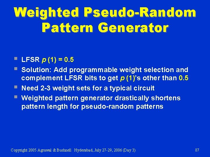
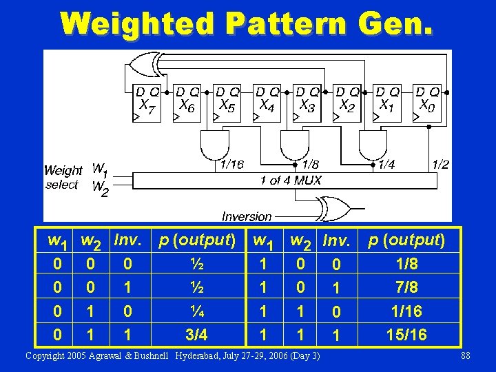
Weighted Pseudo-Random Pattern Generator § § LFSR p (1) = 0. 5 Solution: Add programmable weight selection and complement LFSR bits to get p (1)’s other than 0. 5 Need 2 -3 weight sets for a typical circuit Weighted pattern generator drastically shortens pattern length for pseudo-random patterns Copyright 2005 Agrawal & Bushnell Hyderabad, July 27 -29, 2006 (Day 3) 87

Weighted Pattern Gen. w 1 w 2 Inv. p (output) 0 0 0 ½ 0 0 1 ½ 0 1 0 ¼ 0 1 1 3/4 w 1 w 2 Inv. 1 0 0 1 1 1 Copyright 2005 Agrawal & Bushnell Hyderabad, July 27 -29, 2006 (Day 3) p (output) 1/8 7/8 1/16 15/16 88

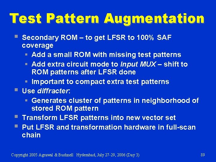
Test Pattern Augmentation § § Secondary ROM – to get LFSR to 100% SAF coverage § Add a small ROM with missing test patterns § Add extra circuit mode to Input MUX – shift to ROM patterns after LFSR done § Important to compact extra test patterns Use diffracter: § Generates cluster of patterns in neighborhood of stored ROM pattern Transform LFSR patterns into new vector set Put LFSR and transformation hardware in full-scan chain Copyright 2005 Agrawal & Bushnell Hyderabad, July 27 -29, 2006 (Day 3) 89

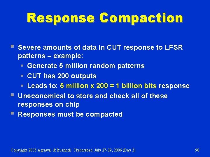
Response Compaction § § § Severe amounts of data in CUT response to LFSR patterns – example: § Generate 5 million random patterns § CUT has 200 outputs § Leads to: 5 million x 200 = 1 billion bits response Uneconomical to store and check all of these responses on chip Responses must be compacted Copyright 2005 Agrawal & Bushnell Hyderabad, July 27 -29, 2006 (Day 3) 90

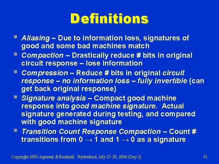
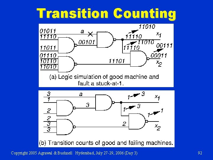
Definitions § § § Aliasing – Due to information loss, signatures of good and some bad machines match Compaction – Drastically reduce # bits in original circuit response – lose information Compression – Reduce # bits in original circuit response – no information loss – fully invertible (can get back original response) Signature analysis – Compact good machine response into good machine signature. Actual signature generated during testing, and compared with good machine signature Transition Count Response Compaction – Count # transitions from 0 → 1 and 1 → 0 as a signature Copyright 2005 Agrawal & Bushnell Hyderabad, July 27 -29, 2006 (Day 3) 91

Transition Counting Copyright 2005 Agrawal & Bushnell Hyderabad, July 27 -29, 2006 (Day 3) 92

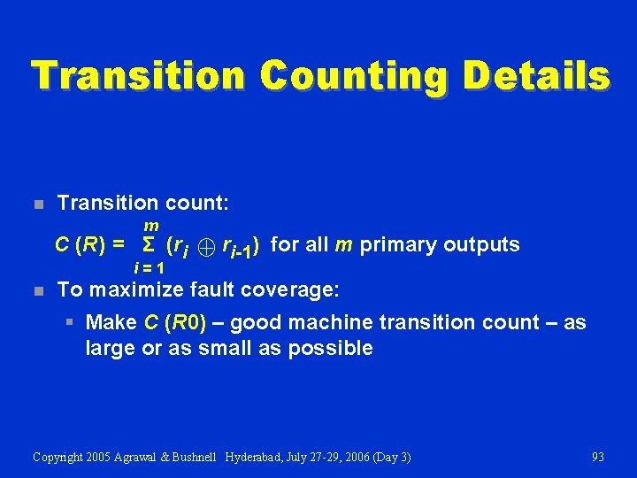
Transition Counting Details n Transition count: m C (R) = Σ (ri i=1 n Å ri-1) for all m primary outputs To maximize fault coverage: § Make C (R 0) – good machine transition count – as large or as small as possible Copyright 2005 Agrawal & Bushnell Hyderabad, July 27 -29, 2006 (Day 3) 93

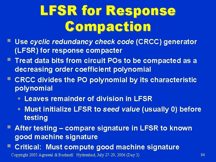
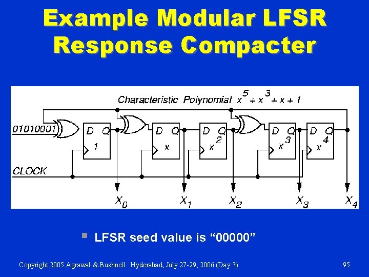
§ § § LFSR for Response Compaction Use cyclic redundancy check code (CRCC) generator (LFSR) for response compacter Treat data bits from circuit POs to be compacted as a decreasing order coefficient polynomial CRCC divides the PO polynomial by its characteristic polynomial § Leaves remainder of division in LFSR § Must initialize LFSR to seed value (usually 0) before testing After testing – compare signature in LFSR to known good machine signature Critical: Must compute good machine signature Copyright 2005 Agrawal & Bushnell Hyderabad, July 27 -29, 2006 (Day 3) 94

Example Modular LFSR Response Compacter § LFSR seed value is “ 00000” Copyright 2005 Agrawal & Bushnell Hyderabad, July 27 -29, 2006 (Day 3) 95

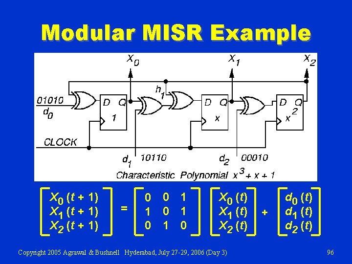
Modular MISR Example X 0 (t + 1) X 1 (t + 1) X 2 (t + 1) = 0 0 1 1 0 1 0 X 0 (t) X 1 (t) X 2 (t) Copyright 2005 Agrawal & Bushnell Hyderabad, July 27 -29, 2006 (Day 3) + d 0 (t) d 1 (t) d 2 (t) 96

Aliasing Theorems § Theorem 15. 1: Assuming that each circuit PO dij has probability p of being in error, and that all outputs dij are independent, in a k-bit MISR, Pal = 1/(2 k), regardless of initial condition of MISR. Not exactly true – true in practice. § Theorem 15. 2: Assuming that each PO dij has probability pj of being in error, where the pj probabilities are independent, and that all outputs dij are independent, in a k-bit MISR, Pal = 1/(2 k), regardless of the initial condition. Copyright 2005 Agrawal & Bushnell Hyderabad, July 27 -29, 2006 (Day 3) 97

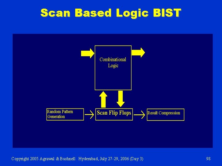
Scan Based Logic BIST Copyright 2005 Agrawal & Bushnell Hyderabad, July 27 -29, 2006 (Day 3) 98

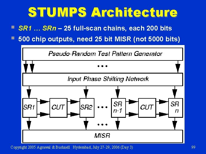
STUMPS Architecture § § SR 1 … SRn – 25 full-scan chains, each 200 bits 500 chip outputs, need 25 bit MISR (not 5000 bits) Copyright 2005 Agrawal & Bushnell Hyderabad, July 27 -29, 2006 (Day 3) 99

STUMPS § § Test procedure: 1. Scan in patterns from LFSR into all scan chains (200 clocks) 2. Switch to normal functional mode and clock 1 x with system clock 3. Scan out chains into MISR (200 clocks) where test results are compacted § Overlap Steps 1 & 3 Requirements: § Every system input is driven by a scan chain § Every system output is caught in a scan chain or drives another chip being sampled Copyright 2005 Agrawal & Bushnell Hyderabad, July 27 -29, 2006 (Day 3) 100

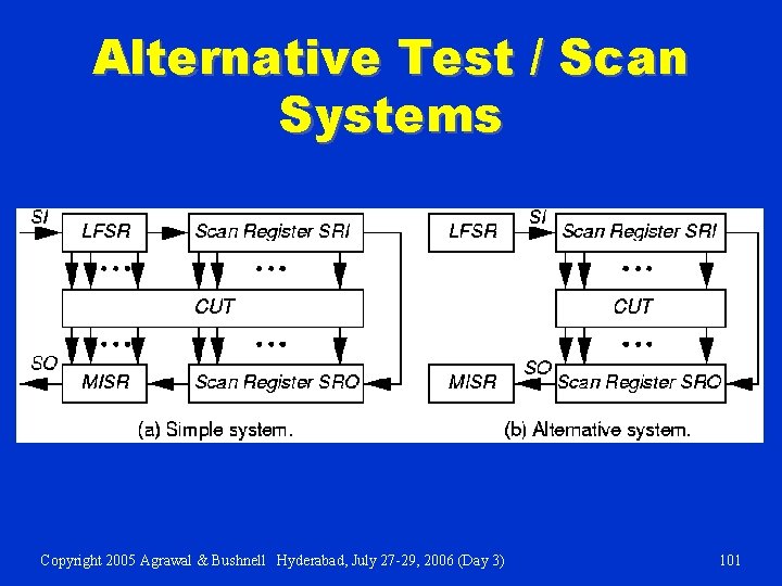
Alternative Test / Scan Systems Copyright 2005 Agrawal & Bushnell Hyderabad, July 27 -29, 2006 (Day 3) 101

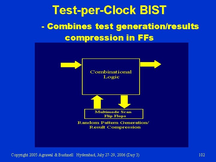
Test-per-Clock BIST - Combines test generation/results compression in FFs Copyright 2005 Agrawal & Bushnell Hyderabad, July 27 -29, 2006 (Day 3) 102

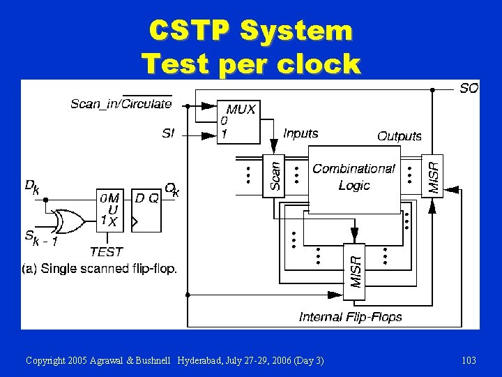
CSTP System Test per clock Copyright 2005 Agrawal & Bushnell Hyderabad, July 27 -29, 2006 (Day 3) 103

Examples of CSTP Systems § § § CSTP BIST for 4 ASICs at Lucent Technologies: § Tested everything on 3 of the 4, except for: § Input/Output buffers and Input MUX BIST overheads: logic – 20 %, chip area – 13 % Stuck-at fault coverage – 92 % Copyright 2005 Agrawal & Bushnell Hyderabad, July 27 -29, 2006 (Day 3) 104

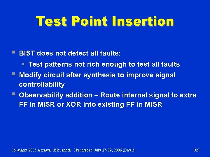
Test Point Insertion § BIST does not detect all faults: § Test patterns not rich enough to test all faults § Modify circuit after synthesis to improve signal controllability § Observability addition – Route internal signal to extra FF in MISR or XOR into existing FF in MISR Copyright 2005 Agrawal & Bushnell Hyderabad, July 27 -29, 2006 (Day 3) 105

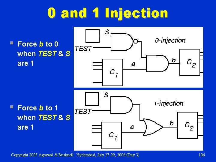
0 and 1 Injection § Force b to 0 when TEST & S are 1 § Force b to 1 when TEST & S are 1 Copyright 2005 Agrawal & Bushnell Hyderabad, July 27 -29, 2006 (Day 3) 106

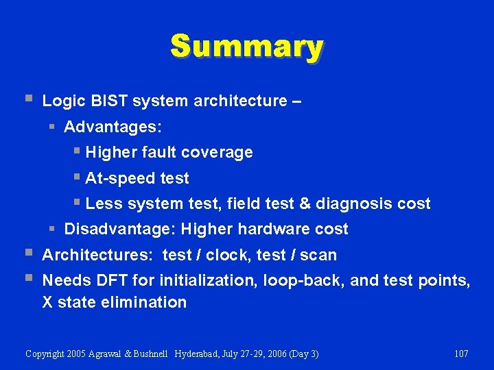
Summary § Logic BIST system architecture – § Advantages: § Higher fault coverage § At-speed test § Less system test, field test & diagnosis cost § Disadvantage: Higher hardware cost § § Architectures: test / clock, test / scan Needs DFT for initialization, loop-back, and test points, X state elimination Copyright 2005 Agrawal & Bushnell Hyderabad, July 27 -29, 2006 (Day 3) 107

Memory BIST Copyright 2005 Agrawal & Bushnell Hyderabad, July 27 -29, 2006 (Day 3) 108

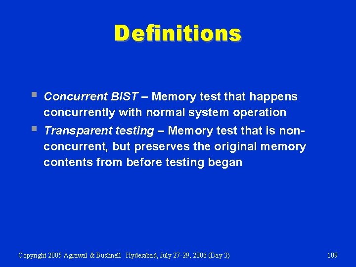
Definitions § Concurrent BIST – Memory test that happens concurrently with normal system operation § Transparent testing – Memory test that is nonconcurrent, but preserves the original memory contents from before testing began Copyright 2005 Agrawal & Bushnell Hyderabad, July 27 -29, 2006 (Day 3) 109

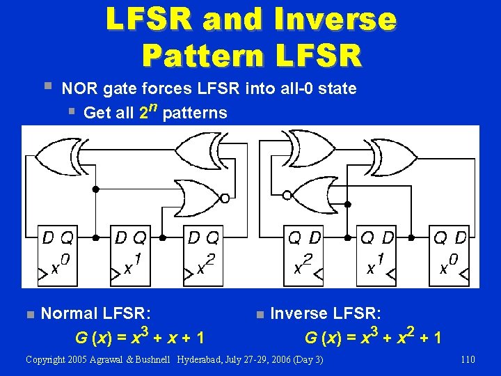
§ n LFSR and Inverse Pattern LFSR NOR gate forces LFSR into all-0 state § Get all 2 n patterns Normal LFSR: G (x) = x 3 + x + 1 n Inverse LFSR: G (x) = x 3 + x 2 + 1 Copyright 2005 Agrawal & Bushnell Hyderabad, July 27 -29, 2006 (Day 3) 110

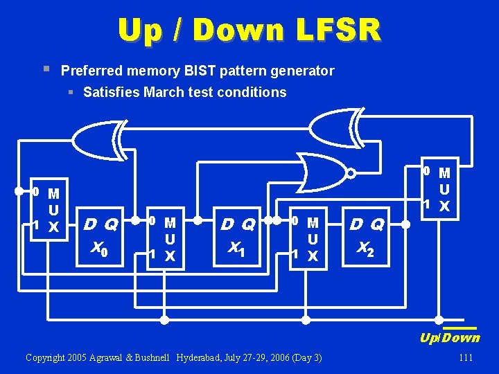
Up / Down LFSR § Preferred memory BIST pattern generator § Satisfies March test conditions 0 M U 1 X D Q X 0 0 M U 1 X D Q X 1 0 M U 1 X D Q U 1 X X 2 Up/Down Copyright 2005 Agrawal & Bushnell Hyderabad, July 27 -29, 2006 (Day 3) 111

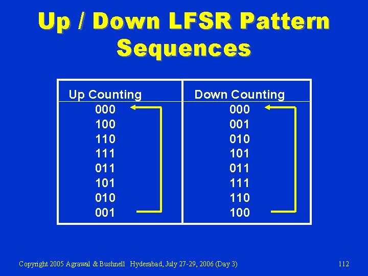
Up / Down LFSR Pattern Sequences Up Counting 000 110 111 011 101 010 001 Down Counting 000 001 010 101 011 110 100 Copyright 2005 Agrawal & Bushnell Hyderabad, July 27 -29, 2006 (Day 3) 112

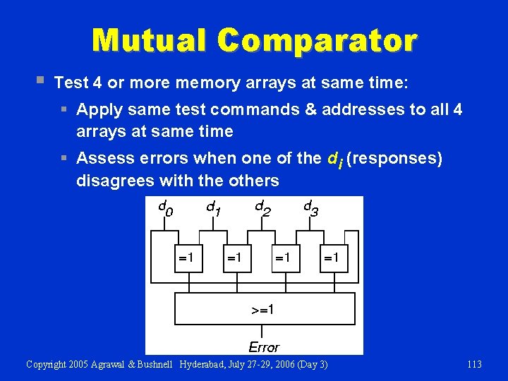
Mutual Comparator § Test 4 or more memory arrays at same time: § Apply same test commands & addresses to all 4 arrays at same time § Assess errors when one of the di (responses) disagrees with the others Copyright 2005 Agrawal & Bushnell Hyderabad, July 27 -29, 2006 (Day 3) 113

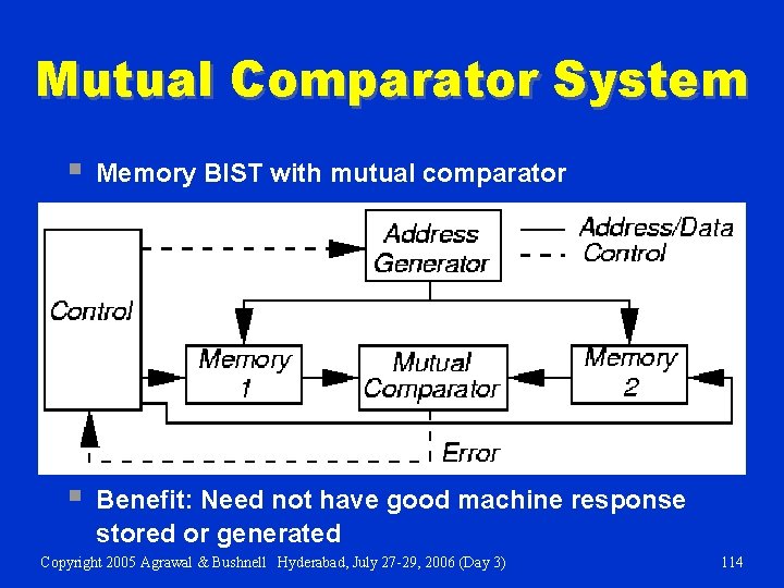
Mutual Comparator System § Memory BIST with mutual comparator § Benefit: Need not have good machine response stored or generated Copyright 2005 Agrawal & Bushnell Hyderabad, July 27 -29, 2006 (Day 3) 114

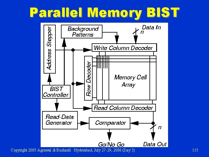
Parallel Memory BIST Copyright 2005 Agrawal & Bushnell Hyderabad, July 27 -29, 2006 (Day 3) 115

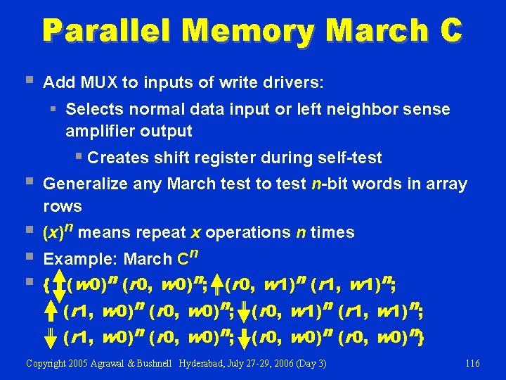
Parallel Memory March C § Add MUX to inputs of write drivers: § Selects normal data input or left neighbor sense amplifier output § Creates shift register during self-test § Generalize any March test to test n-bit words in array rows § § § (x)n means repeat x operations n times Example: March Cn { (w 0)n (r 0, w 0)n; (r 0, w 1)n (r 1, w 1)n; (r 1, w 0)n (r 0, w 0)n; (r 0, w 0)n} Copyright 2005 Agrawal & Bushnell Hyderabad, July 27 -29, 2006 (Day 3) 116

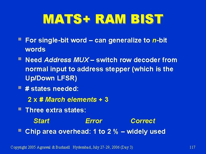
MATS+ RAM BIST § For single-bit word – can generalize to n-bit words § Need Address MUX – switch row decoder from normal input to address stepper (which is the Up/Down LFSR) § # states needed: 2 x # March elements + 3 § Three extra states: Start § Error Correct Chip area overhead: 1 to 2 % – widely used Copyright 2005 Agrawal & Bushnell Hyderabad, July 27 -29, 2006 (Day 3) 117

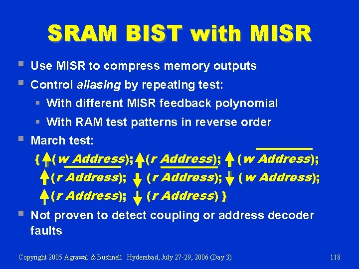
SRAM BIST with MISR § § Use MISR to compress memory outputs Control aliasing by repeating test: § With different MISR feedback polynomial § With RAM test patterns in reverse order § March test: { (w Address); (r Address); § (r Address); (r Address) } (w Address); Not proven to detect coupling or address decoder faults Copyright 2005 Agrawal & Bushnell Hyderabad, July 27 -29, 2006 (Day 3) 118

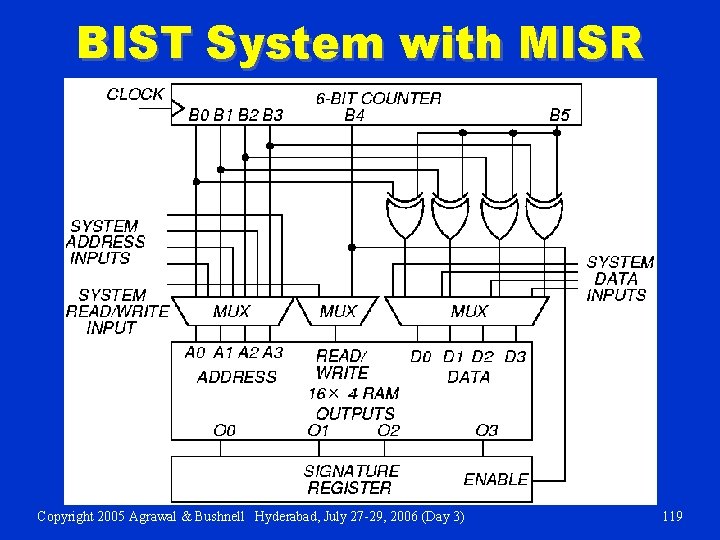
BIST System with MISR Copyright 2005 Agrawal & Bushnell Hyderabad, July 27 -29, 2006 (Day 3) 119

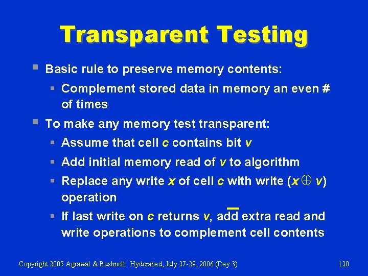
Transparent Testing § Basic rule to preserve memory contents: § Complement stored data in memory an even # of times § To make any memory test transparent: § Assume that cell c contains bit v § Add initial memory read of v to algorithm § Replace any write x of cell c with write (x Å v) operation § If last write on c returns v, add extra read and write operations to complement cell contents Copyright 2005 Agrawal & Bushnell Hyderabad, July 27 -29, 2006 (Day 3) 120

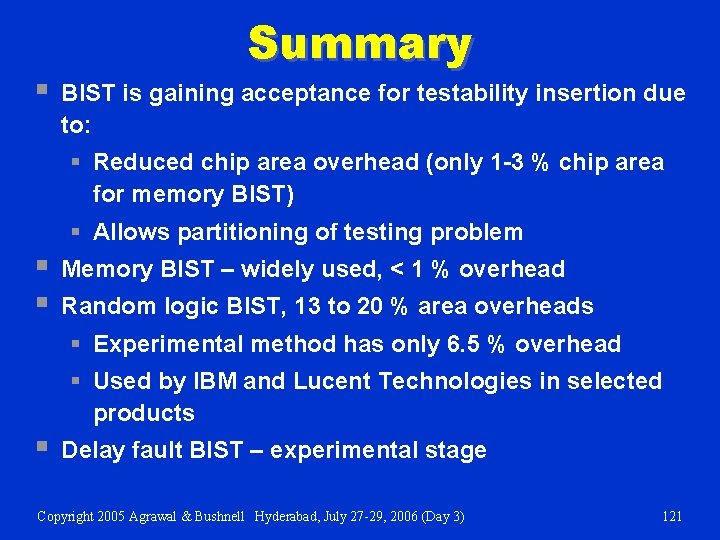
§ Summary BIST is gaining acceptance for testability insertion due to: § Reduced chip area overhead (only 1 -3 % chip area for memory BIST) § Allows partitioning of testing problem § § Memory BIST – widely used, < 1 % overhead Random logic BIST, 13 to 20 % area overheads § Experimental method has only 6. 5 % overhead § Used by IBM and Lucent Technologies in selected products § Delay fault BIST – experimental stage Copyright 2005 Agrawal & Bushnell Hyderabad, July 27 -29, 2006 (Day 3) 121

Test Compression Copyright 2005 Agrawal & Bushnell Hyderabad, July 27 -29, 2006 (Day 3) 122

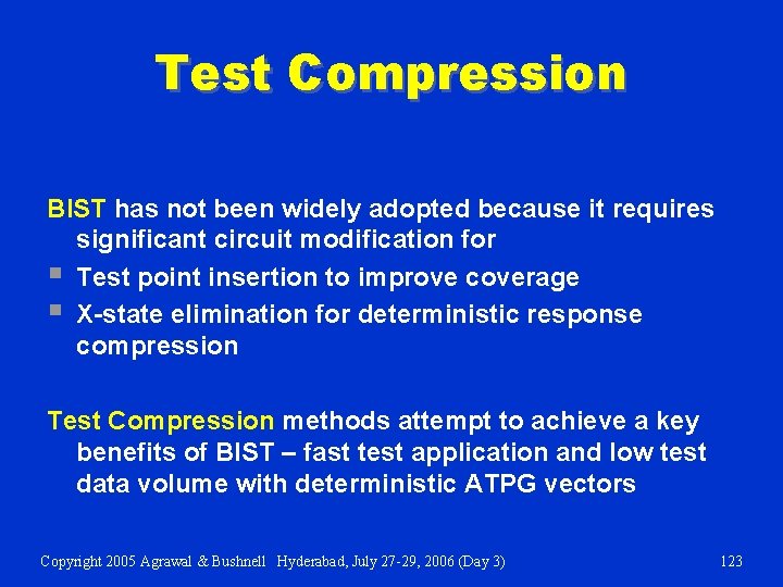
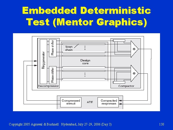
Test Compression BIST has not been widely adopted because it requires significant circuit modification for § Test point insertion to improve coverage § X-state elimination for deterministic response compression Test Compression methods attempt to achieve a key benefits of BIST – fast test application and low test data volume with deterministic ATPG vectors Copyright 2005 Agrawal & Bushnell Hyderabad, July 27 -29, 2006 (Day 3) 123

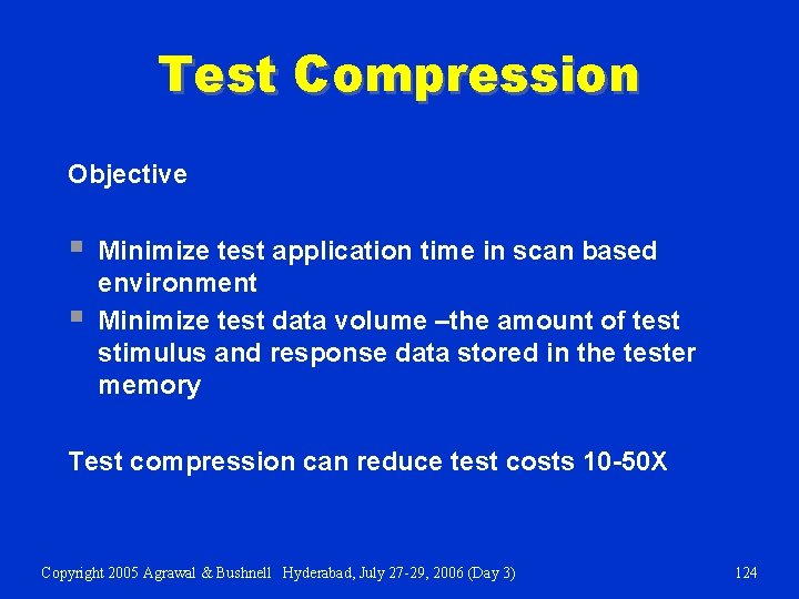
Test Compression Objective § § Minimize test application time in scan based environment Minimize test data volume –the amount of test stimulus and response data stored in the tester memory Test compression can reduce test costs 10 -50 X Copyright 2005 Agrawal & Bushnell Hyderabad, July 27 -29, 2006 (Day 3) 124

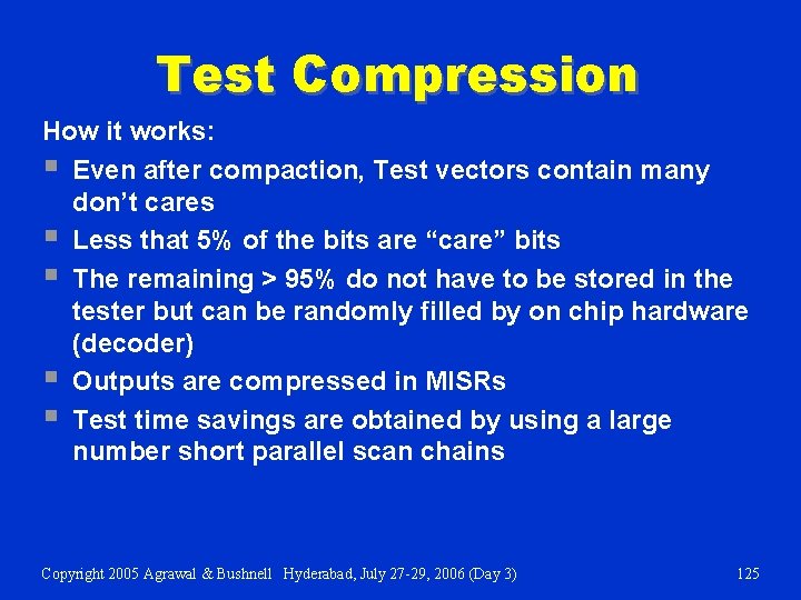
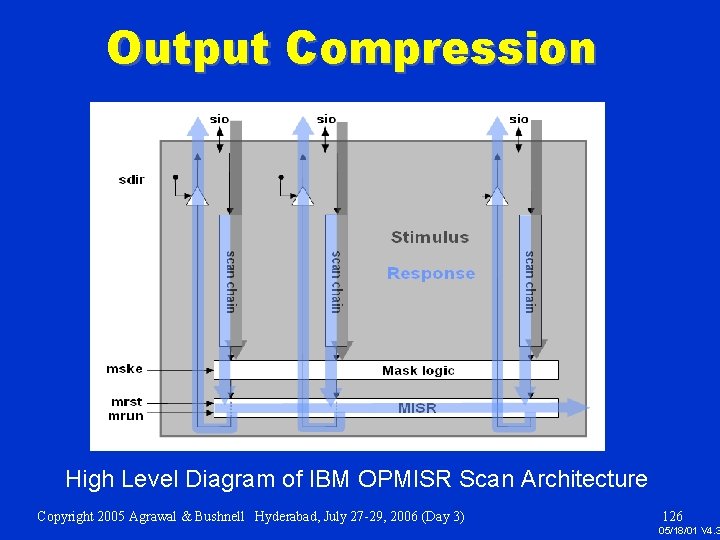
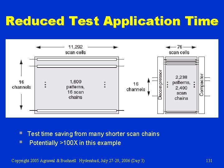
Test Compression How it works: § Even after compaction, Test vectors contain many don’t cares § Less that 5% of the bits are “care” bits § The remaining > 95% do not have to be stored in the tester but can be randomly filled by on chip hardware (decoder) § Outputs are compressed in MISRs § Test time savings are obtained by using a large number short parallel scan chains Copyright 2005 Agrawal & Bushnell Hyderabad, July 27 -29, 2006 (Day 3) 125

Output Compression High Level Diagram of IBM OPMISR Scan Architecture Copyright 2005 Agrawal & Bushnell Hyderabad, July 27 -29, 2006 (Day 3) 126 05/18/01 V 4. 3

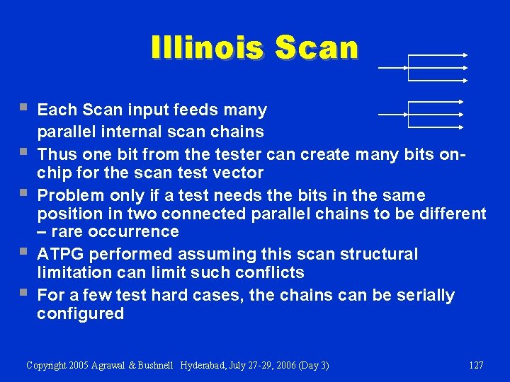
Illinois Scan § § § Each Scan input feeds many parallel internal scan chains Thus one bit from the tester can create many bits onchip for the scan test vector Problem only if a test needs the bits in the same position in two connected parallel chains to be different – rare occurrence ATPG performed assuming this scan structural limitation can limit such conflicts For a few test hard cases, the chains can be serially configured Copyright 2005 Agrawal & Bushnell Hyderabad, July 27 -29, 2006 (Day 3) 127

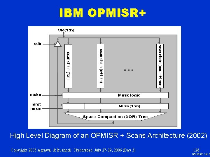
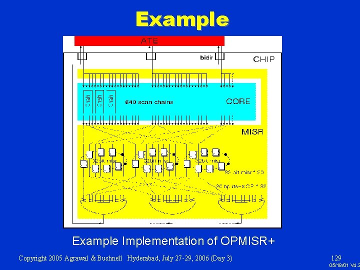
IBM OPMISR+ High Level Diagram of an OPMISR + Scans Architecture (2002) Copyright 2005 Agrawal & Bushnell Hyderabad, July 27 -29, 2006 (Day 3) 128 05/18/01 V 4. 3

Example Implementation of OPMISR+ Copyright 2005 Agrawal & Bushnell Hyderabad, July 27 -29, 2006 (Day 3) 129 05/18/01 V 4. 3

Embedded Deterministic Test (Mentor Graphics) Copyright 2005 Agrawal & Bushnell Hyderabad, July 27 -29, 2006 (Day 3) 130

Reduced Test Application Time § § Test time saving from many shorter scan chains Potentially >100 X in this example Copyright 2005 Agrawal & Bushnell Hyderabad, July 27 -29, 2006 (Day 3) 131

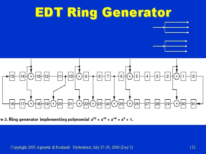
EDT Ring Generator Copyright 2005 Agrawal & Bushnell Hyderabad, July 27 -29, 2006 (Day 3) 132

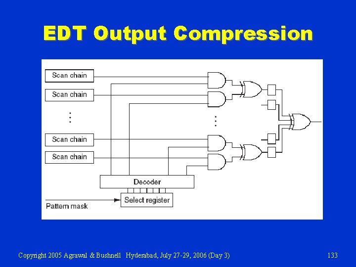
EDT Output Compression Copyright 2005 Agrawal & Bushnell Hyderabad, July 27 -29, 2006 (Day 3) 133

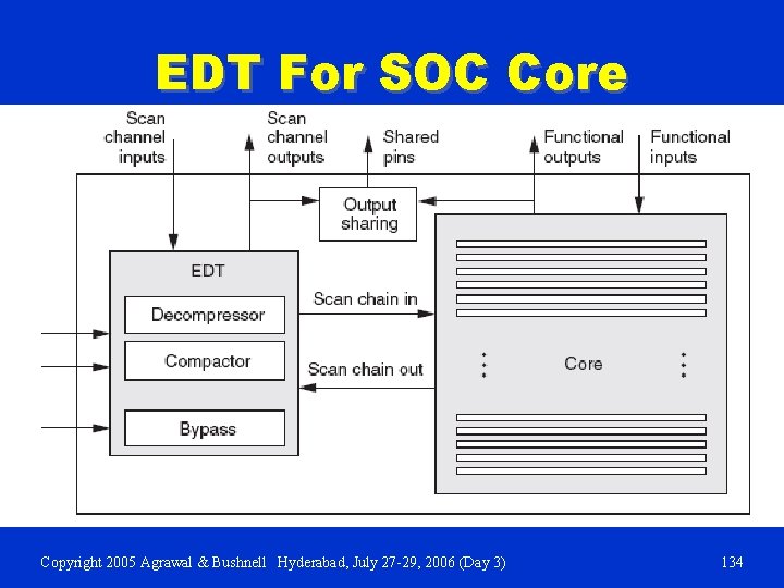
EDT For SOC Core Copyright 2005 Agrawal & Bushnell Hyderabad, July 27 -29, 2006 (Day 3) 134

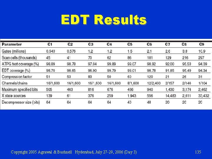
EDT Results Copyright 2005 Agrawal & Bushnell Hyderabad, July 27 -29, 2006 (Day 3) 135