Memory System Design 1 Basic Concepts In this
Memory System Design 1 - Basic Concepts: In this section, we introduce a number of fundamental concepts that relate to the memory hierarchy of a computer. . v Memory Hierarchy a typical memory hierarchy starts with a small, expensive, and relatively fast unit, called the cache, followed by a larger, less expensive, and relatively slow main memory unit. Cache and main memory are built using solid-state semiconductor material. It is customary to call the fast memory level the primary memory. The solid-state memory is followed by larger, less expensive, and far slower magnetic memories that consist typically of the (hard) disk and the tape. It is customary to call the disk the secondary memory, while the tape is conventionally called the tertiary memory. The objective behind designing a memory hierarchy is to have a memory system that performs as if it consists entirely of the fastest unit and whose cost is dominated by the cost of the slowest unit. The memory hierarchy can be characterized by a number of parameters.
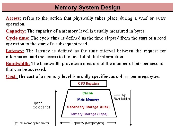
Memory System Design Access: refers to the action that physically takes place during a read or write operation. Capacity: The capacity of a memory level is usually measured in bytes. Cycle time: The cycle time is defined as the time elapsed from the start of a read operation to the start of a subsequent read. Latency: The latency is defined as the time interval between the request for information and the access to the first bit of that information. Bandwidth: The bandwidth provides a measure of the number of bits per second that can be accessed. Cost: The cost of a memory level is usually specified as dollars per megabytes. CPU Registers Cache Speed Cost per bit Main Memory Secondary Storage (Disk) Tertiary Storage (Tape) Typical memory hierarchy Capacity (Megabytes) Latency Bandwidth
Memory System Design Random access refers to the fact that any access to any memory location takes the same fixed amount of time regardless of the actual memory location and/or the sequence of accesses that takes place. Example: If a write operation to memory location 100 takes 15 ns and if this operation is followed by a read operation to memory location 3000, then the latter operation will also take 15 ns. The effectiveness of a memory hierarchy depends on the principle of moving information into the fast memory infrequently and accessing it many times before replacing it with new information. This principle is possible due to a phenomenon called locality of reference.
Memory System Design There exist two forms of locality: spatial and temporal locality. Spatial locality refers to the phenomenon that when a given address has been referenced, it is most likely that addresses near it will be referenced within a short period of time, for example, consecutive instructions in a straight-line program. Temporal locality refers to the phenomenon that once a particular memory item has been referenced, it is most likely that it will be referenced next, for example, an instruction in a program loop.
Memory System Design The sequence of events that takes place when the processor makes a request for an item is as follows. First : the item is sought in the first memory level of the memory hierarchy. Ø The probability of finding the requested item in the first level is called the hit ratio, h 1. Ø The probability of not finding (missing) the requested item in the first level of the memory hierarchy is called the miss ratio, (1 -h 1). When the requested item causes a “miss”, it is sought in the next subsequent memory level. Ø The probability of finding the requested item in the second memory level, the hit ratio of the second level, is h 2. Ø The miss ratio of the second memory level is (1 -h 2). The process is repeated until the item is found. Upon finding the requested item, it is brought and sent to the processor.
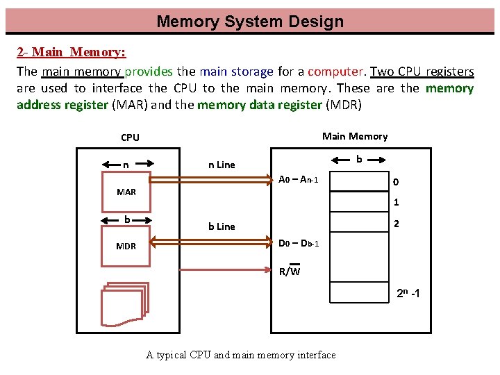
Memory System Design 2 - Main Memory: The main memory provides the main storage for a computer. Two CPU registers are used to interface the CPU to the main memory. These are the memory address register (MAR) and the memory data register (MDR) Main Memory CPU n A 0 – An-1 MAR b MDR b n Line 0 1 2 b Line D 0 – Db-1 R/W 2 n -1 A typical CPU and main memory interface
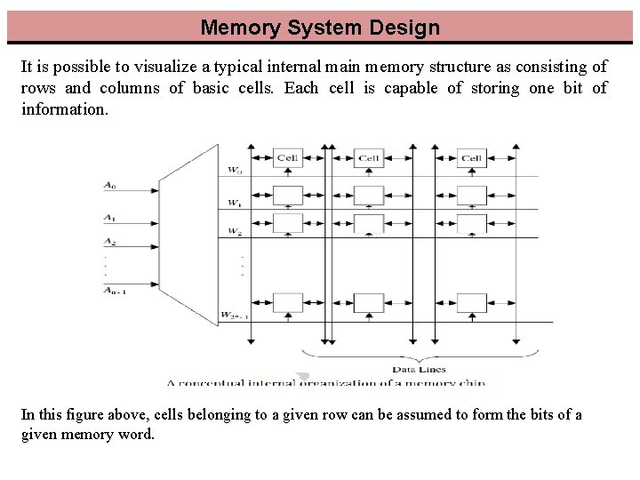
Memory System Design It is possible to visualize a typical internal main memory structure as consisting of rows and columns of basic cells. Each cell is capable of storing one bit of information. In this figure above, cells belonging to a given row can be assumed to form the bits of a given memory word.
Memory System Design Address lines An-1, An-2. . . A 1, A 0 are used as inputs to the address decoder in order to generate the word select lines W 2 n-1. . . W 1, W 0. A given word select line is common to all memory cells in the same row. At any given time, the address decoder activates only one word select line while deactivating the remaining lines. A word select line is used to enable all cells in a row for read or write. Data (bit) lines are used to input or output the contents of cells. Each memory cell is connected to two data lines. A given data line is common to all cells in a given column. Example: a 1 K× 4 memory chip. The memory array should be organized as 1 K rows of cells, each consisting of four cells. The chip will then have to have 10 pins for the address and four pins for the data. However, this may not lead to the best utilization of the chip area.
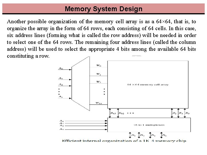
Memory System Design Another possible organization of the memory cell array is as a 64× 64, that is, to organize the array in the form of 64 rows, each consisting of 64 cells. In this case, six address lines (forming what is called the row address) will be needed in order to select one of the 64 rows. The remaining four address lines (called the column address) will be used to select the appropriate 4 bits among the available 64 bits constituting a row.
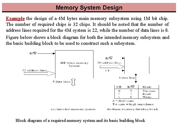
Memory System Design Example the design of a 4 M bytes main memory subsystem using 1 M bit chip. The number of required chips is 32 chips. It should be noted that the number of address lines required for the 4 M system is 22, while the number of data lines is 8. Figure below shows a block diagram for both the intended memory subsystem and the basic building block to be used to construct such a subsystem. Block diagram of a required memory system and its basic building block
- Slides: 10