Memory system 1 Basic Computer Organization Revisited Memory

第五章 Memory system 1
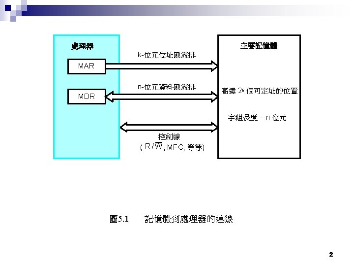

Basic Computer Organization Revisited Memory I/O Data Processor General. Purpose Registers Control Logic MAR ALUs MDR Program PC 3

Access time vs cycle time n Memory access time ¨ n Memory cycle time ¨ n n A measurement of how quickly two back-to-back accesses of a memory chip can be made Cycle time > access time due to latency between successive memory accesses DRAM (For construct Main memory) ¨ ¨ n A measurement of single access time - 50 to 150 nanoseconds require a pause (refresh) between back-to-back accesses SRAM (For construct Cache memory) ¨ ¨ access time - 10 nanoseconds no pause between back-to-back accesses 4

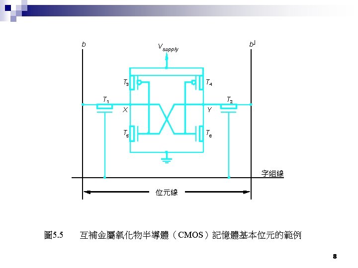
SRAM n SRAM ¨ Static Random Access Memory ¨ Read/write very fast ¨ Needs 6 transistors thus high cost and needs more area ¨ Do not need to refresh ¨ Low power consumption ¨ Implementation technology n CMOS ¨ Construct cache memory 7

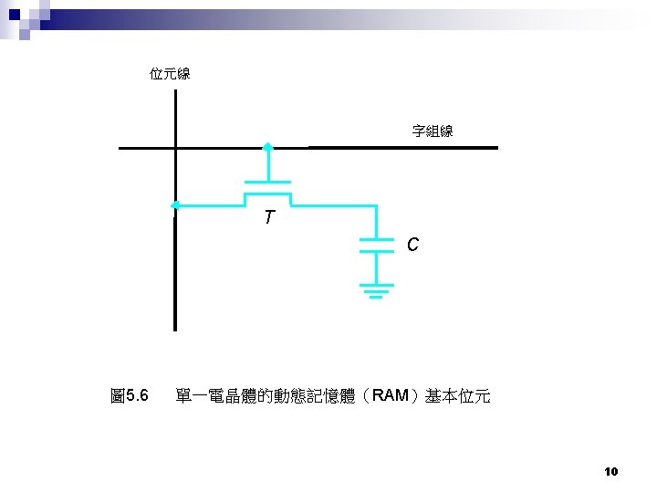
DRAM n DRAM ¨ Dynamic Random Access Memory ¨ Needs 1 transistor and 1 capacitor ¨ Lower cost and compact ¨ Each bit must be refreshed periodically ¨ Implementation technology n CMOS ¨ Construct Main Memory 9
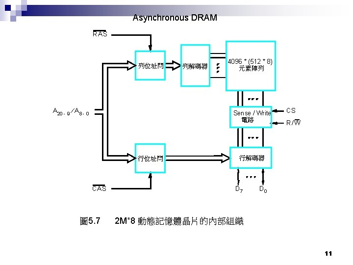

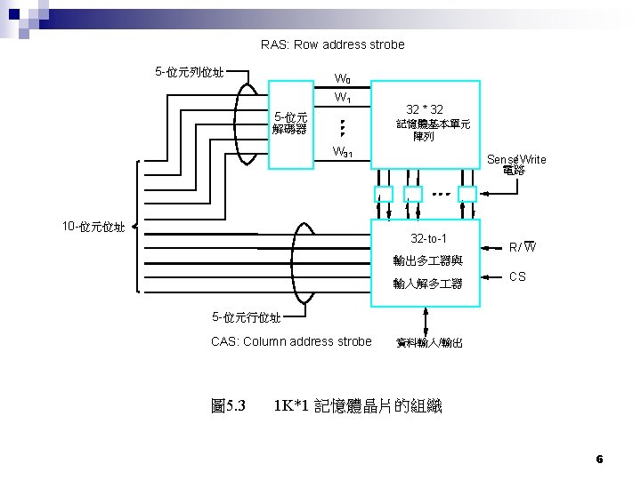
Fast Page Mode conventional DRAM requires that a row and column be sent for each access n FPM works by sending the row address just once for many accesses to memory in locations near each other, improving access time. That is Row address is decoded once with varied Column address decoded to access different bytes on the same row. (見page 5 -54範例5. 1) n 12
 DRAM EDO DRAM n also called hyper page mode DRAM")
Extended Data Out (EDO) DRAM EDO DRAM n also called hyper page mode DRAM n EDO memory has had its timing circuits modified so one access to the memory can begin before the last one has finished (note: conventional DRAM needs some delay between two consecutive accesses) n 13
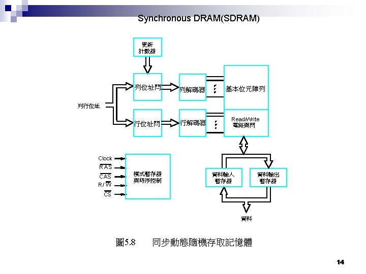

SDRAM n n n Support burst operation Auto Column Address increment, that is do not need external CAS cycle time to select column address Interleaving memory ¨ contains two banks of memory internally instead of one ¨ This allows the second bank to be "precharging" (RAS and CAS activation) while the first bank is transferring data n Will replace older DRAM technologies 15

DDR SDRAM n Double data rate SDRAM ¨ ¨ n n Standard SDRAM takes action only at rising edge of clock DDR II ¨ n Access data both as rising and falling edge of clock Thus doubles the bandwidth of the memory by transfering data twice per clock running at 1/2 clock frequency of the I/O buffers DDR : 100 MHz driven clock -> 100 MHz data buffers -> DDR applied -> 200 MHz final data frequency DDR-II: 100 MHz driven clock -> 200 MHz data buffers -> DDR applied -> 400 MHz final data frequency 16

SIMM vs DIMM n SIMM ¨ Single In-line Memory Modules ¨ 30 pins (8 bit bus version) ¨ 72 pins (wider bus, more address lines) n DIMM ¨ Dual In-line Memory Modules ¨ 168 pins 17

RAMBUS n n RAMBUS Company Make a single chip act more like a memory system than a memory componet Each chip has interleaved memory and high-speed interface RDRAM (1 st generation) Drop RAS/CAS, replacing it with a bus that allows other accesses over the bus between the sending of the address and return of the data. ¨ Run at 300 MHz clock ¨ n DRDRAM (2 nd generation) Direct RDRAM Separate row- and column-command buses instead of the conventional multiplexing ¨ Run at 400 MHz clock ¨ ¨ n RIMM ¨ 16 RDRAM 18

Other memory ROM n PROM n EEPROM n Flash n ¨ Low power consumption ¨ Portable system such as PDA, mobile phone, digital camera, MP 3 19
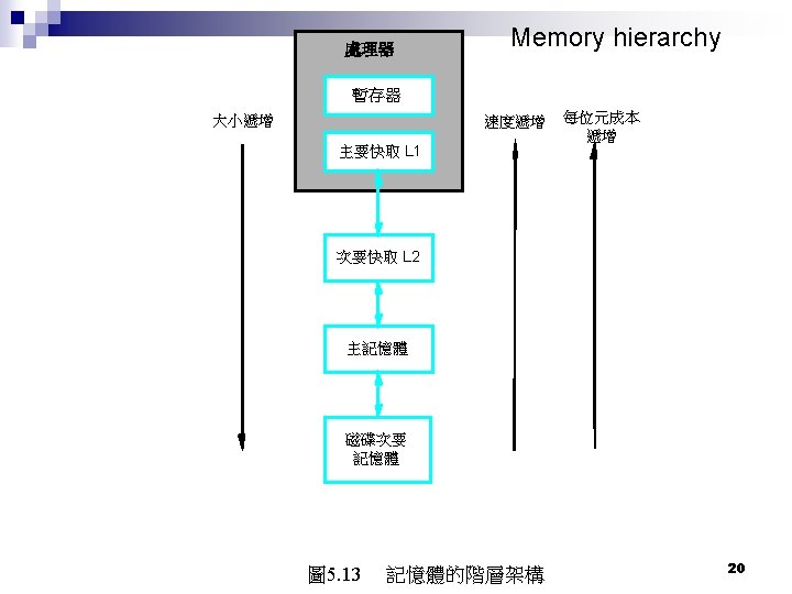

Memory hierarchy n n Level 1 ¨ Registers ¨ <1 KB ¨ 0. 25 -0. 5 ns ¨ 20, 000 -100, 000 MB/sec ¨ Managed by compiler Level 2 ¨ Cache ¨ <16 MB ¨ 0. 5 -25 ns ¨ 5000 -10000 MB/sec ¨ Managed by hardware Level 3 ¨ Main memory ¨ <16 GB ¨ 80 -250 ns ¨ 1000 -5000 MB/sec ¨ Managed by OS Level 4 ¨ Disk storage ¨ >100 GB ¨ 5000000 ns ¨ 20 -150 MB/sec ¨ Managed by OS/operator 21

Cache Terms n Locality of reference Temporal ¨ spatial ¨ n n n Cache block (cache line) Replacement algorithm Read/write hit/miss Write-through Write-back (copy-back) ¨ n Dirty bit/modified bit Valid bit ¨ The valid bit is set every time a row is loaded into the cache by a cache miss, and can only be reset by the flush line 22
 n Fully associative mapping(完全關聯映射) n Set associative mapping (集合關聯映射)")
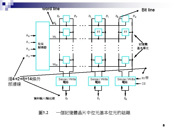
Cache mapping functions Direct mapping(直接映射) n Fully associative mapping(完全關聯映射) n Set associative mapping (集合關聯映射) n ¨ N-way associative mapping 23
 主記憶體 Block 0 Block 1 tag 快取 Block 127 Block")
• Direct mapping(直接映射) 主記憶體 Block 0 Block 1 tag 快取 Block 127 Block 0 Block 128 tag Block 129 tag Block 127 Block 255 Block 256 Block 257 Block 4095 標籤 5 區塊 7 字組 4 圖 5. 15 主記憶體位址 直接映射的快取 24
 主記憶體 Block 0 Block 1 快取 tag Block 0 tag Block")
Fully associative mapping(完全關聯映射) 主記憶體 Block 0 Block 1 快取 tag Block 0 tag Block 1 Block tag i Block 127 Block 4095 標籤 12 圖 5. 16 字組 4 主記憶體位址 關聯式映射的快取 25
 主記憶體 Block 0 Block 1 快取 Set 0 Set 1")
Set associative mapping (集合關聯映射) 主記憶體 Block 0 Block 1 快取 Set 0 Set 1 Set 63 tag tag tag Block 0 Block 63 Block 1 Block 64 Block 2 Block 65 Block 3 Block 127 Block 126 Block 128 Block 127 Block 129 Block 4095 T 標籤 6 圖 5. 17 集合 6 字組 4 主記憶體位址 每個集合有2個區塊的集合關聯式映射快取 26

Replacement algorithm n LRU ¨ Least recently used ¨ 最近最少使用到 n Random ¨ 隨機 n First in First out (FIFO) ¨ 最舊 27

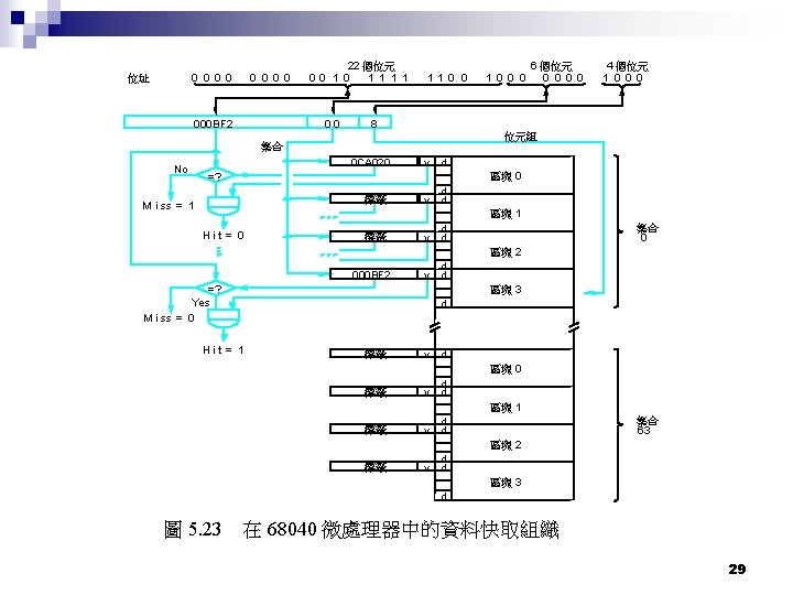
68040 cache n n 4 K Data cache 4 K Instruction cache Contains 64 set Every set contains 4 blocks ¨ 4 -way n n n associative mapping 1 cache block contains 4 long words 1 valid bit for cache block 1 dirty bit for long word Write-back/write-through Random replacement 28

ARM 710 T cache n n Only one cache for both data and instructions 4 KB cache 64 sets 1 set contains 4 blocks ¨ 4 -way n n n associative mapping 1 cache block contains 4 words(32 bits)=16 bytes Write-through Random replacement 30

Pentium III cache n L 1 cache ¨ 16 KB data cache n n ¨ 16 KB instruction cache n n n 2 -way No write strategy due to pure code L 2 cache n n 4 -way Write-back or write-through 512 KB 4 -way Write-back or write-through Coppermine ¨ L 2 cache built in CPU n n 256 KB 8 -way 31

Pentium 4 cache n L 1 cache ¨ 8 KB data cache n n L 2 cache ¨ ¨ ¨ n 4 -way block contains 64 bytes Write-through within CPU 256 KB 8 -way Block contains 128 bytes Write-back L 3 cache ¨ Server-based CPU 32

34

35
 and data buffer register")
Memory Performance Every memory module has address buffer register (ABR) and data buffer register (DBR) n Single module continuous words n Continuous module continuous words n ¨ Interleaved memory ¨ CPU reference to continuous memory accesses multiple module concurrently (lower bits select modules) 36

Caculate miss penalty n n n See p 5 -54 ~p 5 -59 examples Tave= h. C + (1 -h)M , where h: hit rate, M: miss penalty, C: access time for cache Tave=h 1 C 1+(1 -h 1)h 2 C 2+(1 -h 1)(1 -h 2)M, ¨ ¨ ¨ ¨ h 1 hit rate for L 1 cache C 1 access time for L 1 cache h 2 hit rate for L 2 cache C 2 access time for L 2 cache M access time for main memory Note: if h 1=h 2=0. 9 then miss penalty=(1 -9)(1 -. 9)=1% This means if we use two level cache with 0. 9 hit rate then the penalty for main memory will less than 1% memory access 37
 ¨ Built")
Other methods to reduce miss penalty n Write buffer (improvement for write-through) ¨ Built in CPU ¨ Write to write buffer rather than to memory, thus CPU doesn’t need to wait memory write n Prefetch ¨ Compiler codes) n inserts prefetch instructions (via analyzing Lockup-free ¨ Allowing the data cache to continue to supply cache hits during a miss ¨ Helpful for processor that supports out-of-order completion (eg. Via Tomasulo’s Algorithm) 38
 MMU (built in CPU)")
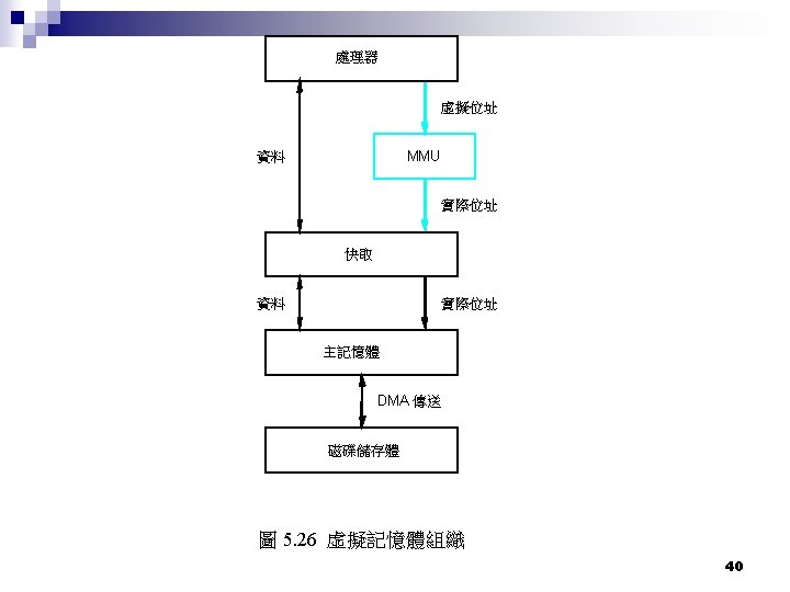
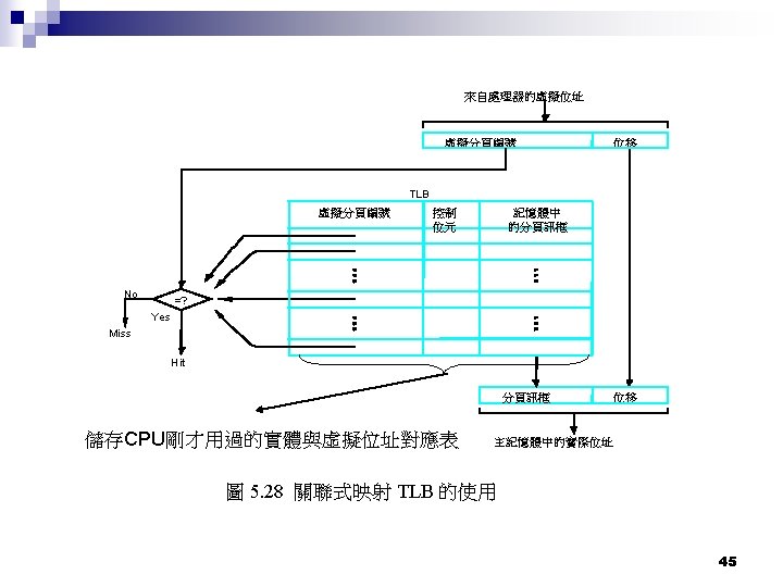
Virtual memory n n n n Virtual address (logical address) MMU (built in CPU) Physical address Page table (in Main Memory) Page frame Address translation TLB ¨ n n Cache built within CPU for holding translated address just used Page fault Replacement algorithm ¨ LRU 39

Intel IA-32 Processor’s Memory management 42

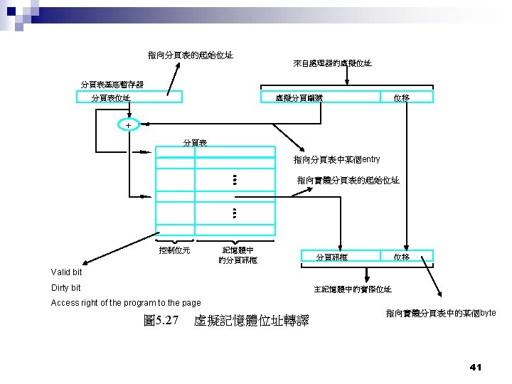
Intel IA-32 Page Translation The entries in the page directory point to page tables, and the entries in a page table point to pages in physical memory. This paging method can be used to address up to 220 pages, which spans a linear address space of 232 bytes (4 GBytes). 43

To select the various table entries, the linear address is divided into three sections: • Page-directory entry—Bits 22 through 31 provide an offset to an entry in the page directory. The selected entry provides the base physical address of a page table. • Page-table entry—Bits 12 through 21 of the linear address provide an offset to an entry in the selected page table. This entry provides the base physical address of a page in physical memory. • Page offset—Bits 0 through 11 provides an offset to a physical address in the page. 44
 n Transfer time n")
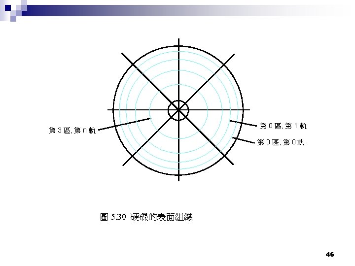
Disk Access Time Seek time n Rotation time (latency time) n Transfer time n 47

RAID Redundant Array of Inexpensive Disk n n n n RAID 0 : data stripping, no redundancy, Level 0 stripes data at block level RAID 1 : mirroring (shadowing) RAID 01(RAID 0+1): mirrored stripes RAID 2 : Error-Correcting Coding with hamming code ¨ Not a typical implementation and rarely used, Level 2 stripes data at the bit level rather than the block level. RAID 3: Bit-Interleaved Parity ¨ Provides byte-level striping with a dedicated parity disk. Level 3, which cannot service simultaneous multiple requests, also is rarely used. RAID 4: Dedicated Parity Drive. ¨ A commonly used implementation of RAID, Level 4 provides block-level striping (like Level 0) with a parity disk. If a data disk fails, the parity data is used to create a replacement disk. A disadvantage to Level 4 is that the parity disk can create write bottlenecks. RAID 5: Block Interleaved Distributed Parity, ¨ Provides data striping at the byte level and also stripe error correction information. This results in excellent performance and good fault tolerance. Level 5 is one of the most popular implementations of RAID. 49
 n n CD-ROM 1 X : 150 KB/sec CD-ROM 40 X:")
Compact Disc (CD) n n CD-ROM 1 X : 150 KB/sec CD-ROM 40 X: 150 x 40 = 6 MB/sec DVD (Digital Versatile Disk) DVD + R ¨ n DVD+R/W ¨ n has some "better" features than DVD-R/W such as lossless linking and both CAV and CLV writing. DVD – R ¨ n is a non-rewritable format and it is compatible with about 89%of all DVD Players and most DVD-ROMs is a non-rewriteable format and it is compatible with about 93% of all DVD Players and most DVD-ROMs. DVD-R/W ¨ was the first DVD recording format released that was compatible with standalone DVD Players. 50

DVD Sizes n DVD-5, holds around 4 700 000 bytes and that is 4. 37 computer GB where 1 kbyte is 1024 bytes*. DVD+R/W and DVD-R/W supports this format. Also called Single Sided Single Layered. This is the most common DVD Media, often called 4. 7 GB Media. DVD-10, holds around 9 400 000 bytes and that is 8. 75 computer GB. DVD+R/W and DVD-R/W supports this format. Also called Double Sided Single Layered. DVD-9, holds around 8 540 000 bytes and that is 7. 95 computer GB. DVD+R supports this format. Also called Single Sided Dual Layered. This media is called DVD+R 9, DVD+R DL or 8. 5 GB Media. DVD-18, holds around 17 080 000 bytes and that is 15. 9 computer GB. DVD+R supports this format. Also called Double Sided Dual Layered. 51
 write speeds 1 x")
DVD Write and read speeds n Single Layer(4. 7 GB) write speeds 1 x (CLV) = about 58 minutes 2 x (CLV) = about 29 minutes 2. 4 x (CLV) = about 24 minutes 4 x (CLV) = about 14. 5 minutes 6 x (CLV/ZCLV) = about 10 -12 minutes 8 x (PCAV/ZCLV) = about 8 -10 minutes 12 x (PCAV/ZCLV) = about 6. 5 -7. 5 minutes 16 x (CAV/ZCLV) = about 6 -7 minutes Dual/Double Layer(8. 5 GB) write speeds 1 x CLV = about 105 minutes 2. 4 x CLV = about 44 minutes 4 x CLV = about 27 minutes Single Layer (4. 7 GB) read speeds 6 x CAV (avg. ~4 x) read speed is max 7. 93 MB/s = ~14 minutes 8 x CAV (avg. ~6 x) read speed is max 10. 57 MB/s = ~10 minutes 12 x CAV (avg. ~8 x) read speed is max 15. 85 MB/s = ~7 minutes 16 x CAV (avg. ~12 x) read speed is max 21. 13 MB/s = ~5 minutes 52
- Slides: 53