MEMORY popo MEMORY Programs and the data are



- Slides: 26

MEMORY popo

MEMORY • Programs and the data are stored in the memory of the computer • Ideally, the memory would be fast, large, and inexpensive. • Unfortunately, it is impossible to meet all three of these requirements simultaneously. • Increased speed and size are achieved at increased cost. • To solve this problem, much work has gone into developing clever structures that improve the speed and size of the memory, yet keep the cost reasonable. popo

MEMORYORGANIZATION • BASIC CONCEPTS • The maximum size of the memory that can be used in any computer is determined by the addressing scheme. • For example, a 16 -bit computer that generates 16 bit addresses is capable of addressing up to 216 = 65536 64 K memory locations. • Similarly, machines whose instructions generate 32 -bit addresses can utilize a memory that contains up to 232 =4 G (giga) memory locations • No of bit that can store word length popo

MEMORYORGANIZATION • The memory is usually designed to store and retrieve data in word-length quantities. • In fact, the number of bits actually stored or retrieved in one memory access is the most common definition of the word length of a computer. • Consider, for example, a byte- addressable computer whose instructions generate 32 -bit addresses. • When a 32 -bit address is sent from the processor to the memory unit, the high-order 30 bits determine which word will be accessed. • If a byte quantity is specified, the low-order 2 bits of the address specify which byte location is involved. popo

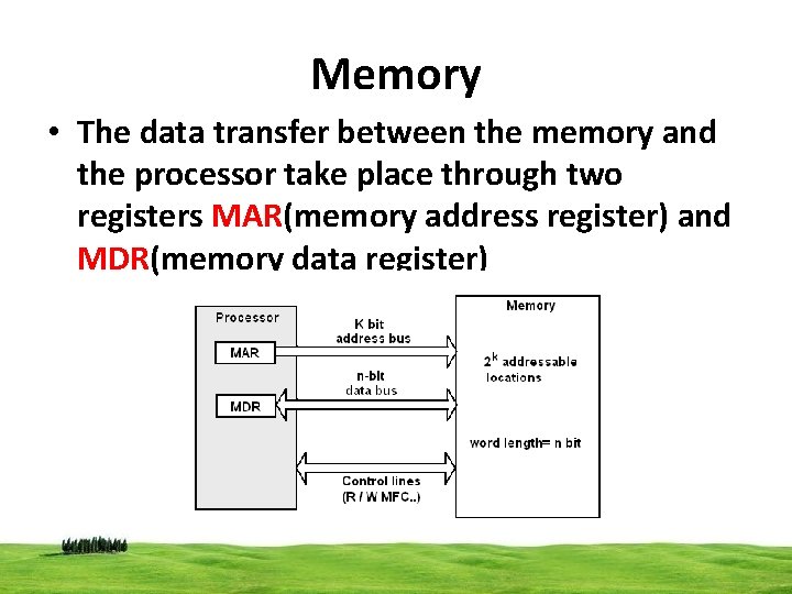
Memory • The data transfer between the memory and the processor take place through two registers MAR(memory address register) and MDR(memory data register)

Memory • If MAR is k bit long and MDR is n bit long, then memory contains up to 2 k addressable locations • Each time n bit of data are transferred between memory and processor • This transfer take place over processor bus, which has k address lines and n data lines • The bus also includes control lines R / W MFC…

Memory • The processor read data from memory by loading the address of the required memory location into MAR and setting R/W’ line to 1 • The memory place the data from the address into data line, and confirm this action by asserting MFC signal • Then processor load data into MDR

Memory • To write data into the memory by loading the address of this location into MAR • Load data into MDR • And setting R/W’ line 0 • Memory access is synchronized by a clock • The time between the Read and MFC memory access time • The minimum time required between the initiation of two successive operations memory cycle time

MEMORYORGANIZATION • A memory unit is called random-access memory (RAM) if any location can be accessed for a Read or Write operation in some fixed amount of time that is independent of the location’s address. • This distinguishes such memory units from serial, or partly serial, access storage devices such as magnetic disks and tapes. • Access time on the latter devices depends on the address or position of the data. • The basic technology for implementing the memory uses semiconductor integrated circuits. popo

MEMORYORGANIZATION • One way to reduce the memory access time is to use a cache memory. • This is a small, fast memory that is inserted between the larger, slower main memory and the processor. • It holds the currently active segments of a program and their data. • Virtual memory is another important concept related to memory organization. • So far, we have assumed that the addresses generated by the processor directly specify physical locations in the memory. • This may not always be the case. popo

MEMORYORGANIZATION • The memory control circuitry translates the address specified by the program into an address that can be used to access the physical memory. • In such a case, an address generated by the processor is referred to as a virtual or logical address. • The virtual address space is mapped onto the physical memory where data are actually stored. • The mapping function is implemented by a special memory control circuit, often called the memory management unit. • This mapping function can be changed during program execution according to system requirements. popo

Internal Organization of Memory popo

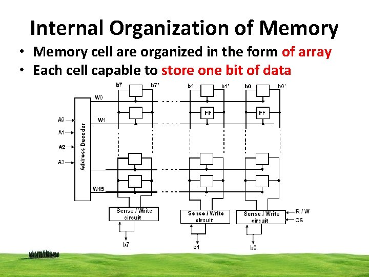
Internal Organization of Memory • Memory cell are organized in the form of array • Each cell capable to store one bit of data

Internal Organization of Memory • Each row of cell contains one word • And all cell of a row contains a common line referred to as word line • Cell in each col are connected to sense/write circuit by 2 bit lines • Sense/ write circuits are connected to the data input/output lines

Internal Organization of Memory • The fig is an example of very small memory chip consisting of 16 words of 8 bit each (16 X 8) organization • The data input and data output of each sense/write circuit are connected to a single bidirectional data line that can be connected to the data bus of a computer • Two control lines R/W’ and CS are provided in addition to address and the data line • The R/W’(read/write’) input specifies the required operation and the CS(chip select) input selects a given chip in a multichip memory system.

Speed, Size and Cost

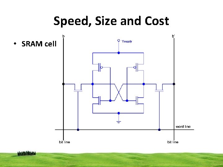
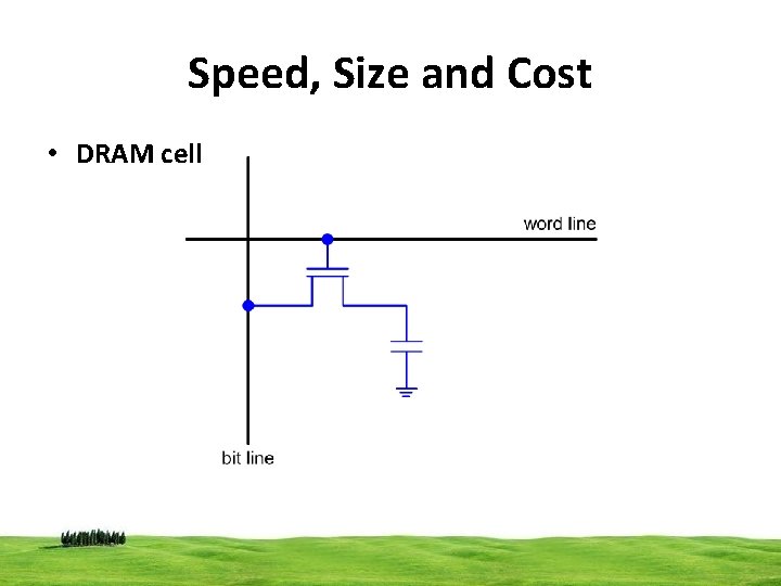
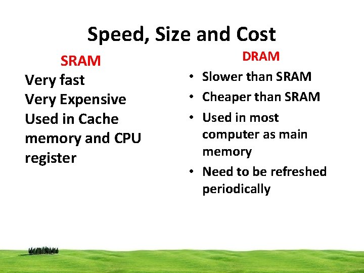
Speed, Size and Cost • An ideal memory would be fast, large and inexpensive • Very fast memory can be implemented if SRAM chips are used ( very expensive, each cell have six transistors) • Then Dynamic RAM chips have much simpler basic cells and thus are much less expensive • But some memories are very slower

Speed, Size and Cost • SRAM cell

Speed, Size and Cost • DRAM cell

Speed, Size and Cost SRAM Very fast Very Expensive Used in Cache memory and CPU register • • DRAM Slower than SRAM Cheaper than SRAM Used in most computer as main memory Need to be refreshed periodically

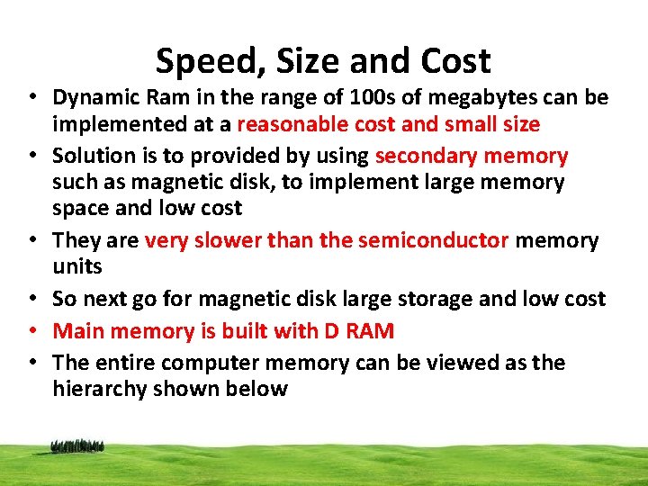
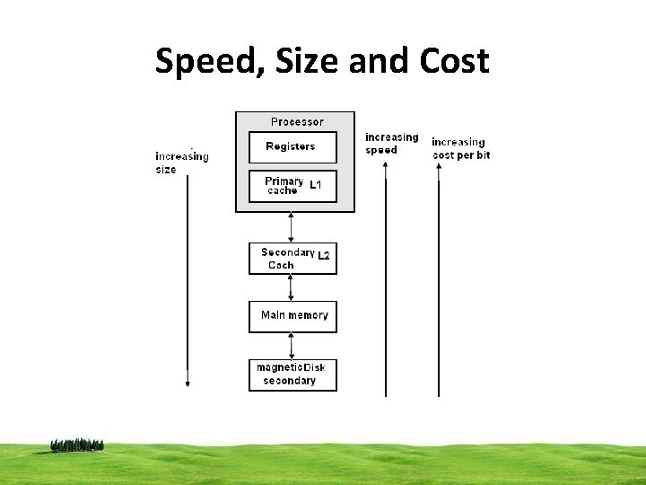
Speed, Size and Cost • Dynamic Ram in the range of 100 s of megabytes can be implemented at a reasonable cost and small size • Solution is to provided by using secondary memory such as magnetic disk, to implement large memory space and low cost • They are very slower than the semiconductor memory units • So next go for magnetic disk large storage and low cost • Main memory is built with D RAM • The entire computer memory can be viewed as the hierarchy shown below

Speed, Size and Cost

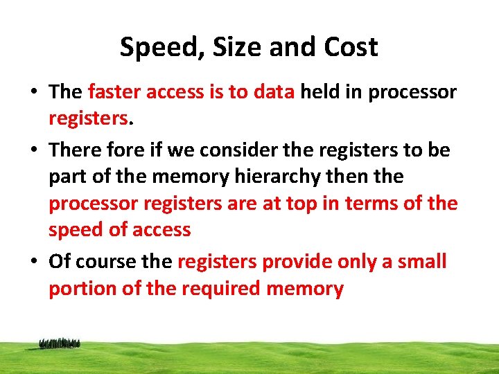
Speed, Size and Cost • The faster access is to data held in processor registers. • There fore if we consider the registers to be part of the memory hierarchy then the processor registers are at top in terms of the speed of access • Of course the registers provide only a small portion of the required memory

Speed, Size and Cost • The processor cache holds copies of instructions and data stored in a much larger memory that is provided externally • Two levels of caches • A primary cache located in the processor chip it referred to as level L 1 cache • A large secondary cache is placed between the primary cache and the rest of memory referred as level L 2 • In some system both L 1 and L 2 caches on processor chip

Speed, Size and Cost • Next level in the hierarchy is main memory • Large memory implemented using Dynamic memory components • Main memory is large but slower than the cache memory • Disk devices provided a huge amount inexpensive storage, very slow compared to semiconductor devices

MEMORYORGANIZATION popo