Memory Organization Adapted from Computer Organization and Design
- Slides: 74

Memory Organization [Adapted from Computer Organization and Design, Patterson & Hennessy, © 2005, and Irwin, PSU 2005]

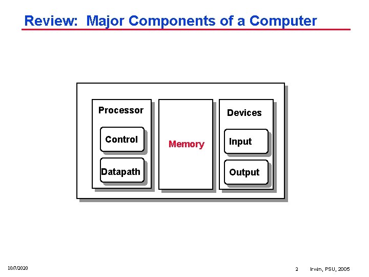
Review: Major Components of a Computer Processor Control Datapath 10/7/2020 Devices Memory Input Output 2 Irwin, PSU, 2005

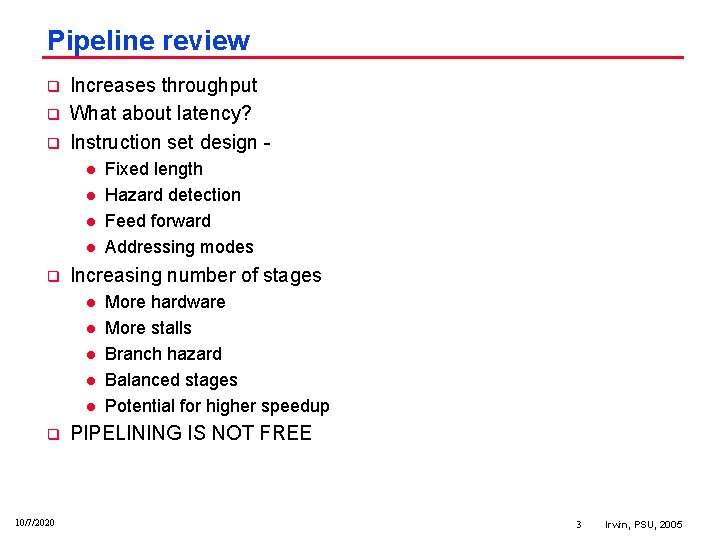
Pipeline review q q q Increases throughput What about latency? Instruction set design l l q Increasing number of stages l l l q 10/7/2020 Fixed length Hazard detection Feed forward Addressing modes More hardware More stalls Branch hazard Balanced stages Potential for higher speedup PIPELINING IS NOT FREE 3 Irwin, PSU, 2005

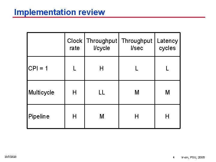
Implementation review Clock Throughput Latency rate I/cycle I/sec cycles 10/7/2020 CPI = 1 L H L L Multicycle H LL M M Pipeline H M H H 4 Irwin, PSU, 2005

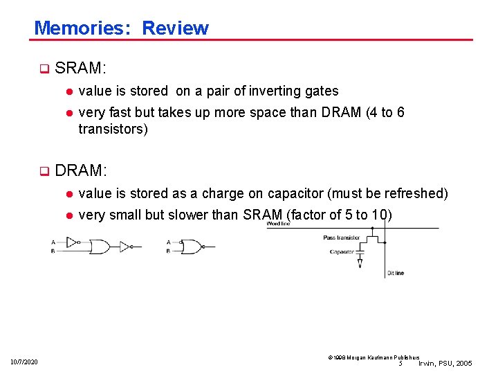
Memories: Review q q 10/7/2020 SRAM: l value is stored on a pair of inverting gates l very fast but takes up more space than DRAM (4 to 6 transistors) DRAM: l value is stored as a charge on capacitor (must be refreshed) l very small but slower than SRAM (factor of 5 to 10) Ó 1998 Morgan Kaufmann Publishers 5 Irwin, PSU, 2005

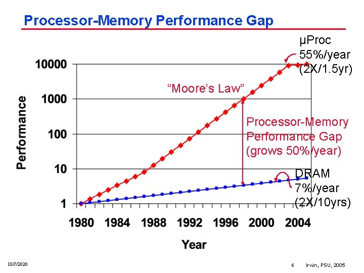
Processor-Memory Performance Gap µProc 55%/year (2 X/1. 5 yr) “Moore’s Law” Processor Memory Performance Gap (grows 50%/year) DRAM 7%/year (2 X/10 yrs) 10/7/2020 6 Irwin, PSU, 2005

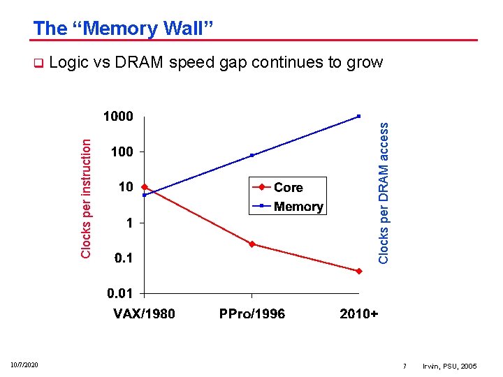
The “Memory Wall” 10/7/2020 Clocks per DRAM access Logic vs DRAM speed gap continues to grow Clocks per instruction q 7 Irwin, PSU, 2005

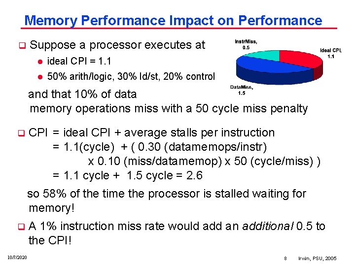
Memory Performance Impact on Performance Suppose a processor executes at q l ideal CPI = 1. 1 l 50% arith/logic, 30% ld/st, 20% control and that 10% of data memory operations miss with a 50 cycle miss penalty CPI = ideal CPI + average stalls per instruction = 1. 1(cycle) + ( 0. 30 (datamemops/instr) x 0. 10 (miss/datamemop) x 50 (cycle/miss) ) = 1. 1 cycle + 1. 5 cycle = 2. 6 q so 58% of the time the processor is stalled waiting for memory! q 10/7/2020 A 1% instruction miss rate would add an additional 0. 5 to the CPI! 8 Irwin, PSU, 2005

The Memory Hierarchy Goal q Fact: Large memories are slow and fast memories are small q How do we create a memory that gives the illusion of being large, cheap and fast (most of the time)? 10/7/2020 l With hierarchy l With parallelism 9 Irwin, PSU, 2005

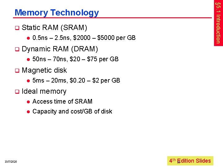
§ 5. 1 Introduction Memory Technology q Static RAM (SRAM) l q Dynamic RAM (DRAM) l q 10/7/2020 50 ns – 70 ns, $20 – $75 per GB Magnetic disk l q 0. 5 ns – 2. 5 ns, $2000 – $5000 per GB 5 ms – 20 ms, $0. 20 – $2 per GB Ideal memory l Access time of SRAM l Capacity and cost/GB of disk 4 th Edition Irwin, Slides PSU, 2005 10

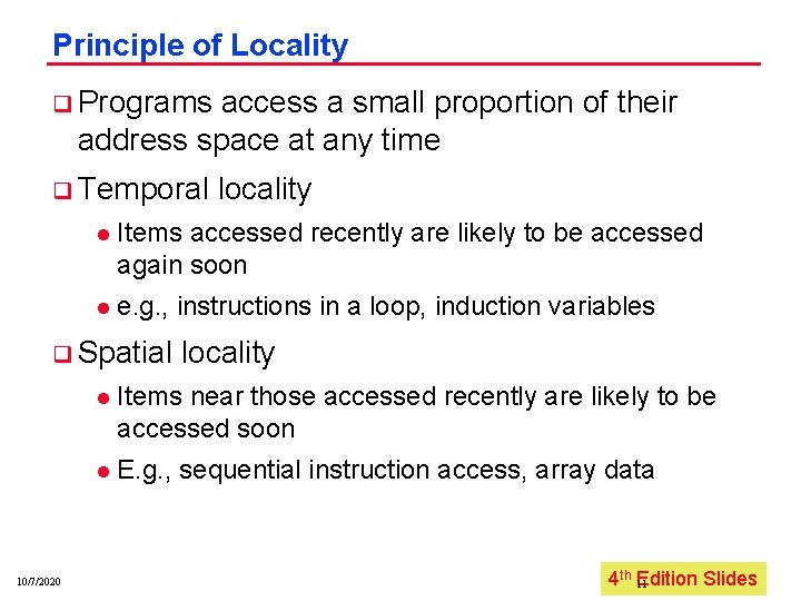
Principle of Locality q Programs access a small proportion of their address space at any time q Temporal l Items accessed recently are likely to be accessed again soon l e. g. , instructions in a loop, induction variables q Spatial 10/7/2020 locality l Items near those accessed recently are likely to be accessed soon l E. g. , sequential instruction access, array data 4 th Edition Irwin, Slides PSU, 2005 11

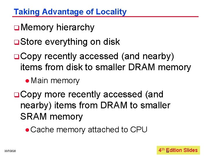
Taking Advantage of Locality q Memory q Store hierarchy everything on disk q Copy recently accessed (and nearby) items from disk to smaller DRAM memory l Main memory q Copy more recently accessed (and nearby) items from DRAM to smaller SRAM memory l Cache 10/7/2020 memory attached to CPU 4 th Edition Irwin, Slides PSU, 2005 12

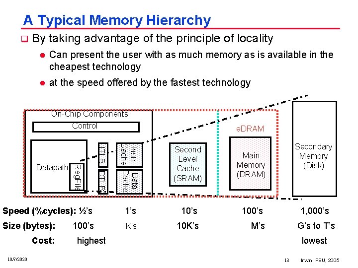
A Typical Memory Hierarchy q By taking advantage of the principle of locality l Can present the user with as much memory as is available in the cheapest technology l at the speed offered by the fastest technology On Chip Components Control e. DRAM Instr Data Cache 1’s 100’s Size (bytes): K’s 10 K’s M’s Cost: 10/7/2020 ITLB DTLB Speed (%cycles): ½’s Datapath Reg. File Second Level Cache (SRAM) 100’s Main Memory (DRAM) Secondary Memory (Disk) 1, 000’s G’s to T’s highest lowest 13 Irwin, PSU, 2005

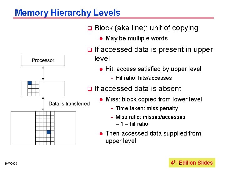
Memory Hierarchy Levels q Block (aka line): unit of copying l q May be multiple words If accessed data is present in upper level l Hit: access satisfied by upper level Hit ratio: hits/accesses q If accessed data is absent l Miss: block copied from lower level Time taken: miss penalty Miss ratio: misses/accesses = 1 – hit ratio l 10/7/2020 Then accessed data supplied from upper level 4 th Edition Irwin, Slides PSU, 2005 14

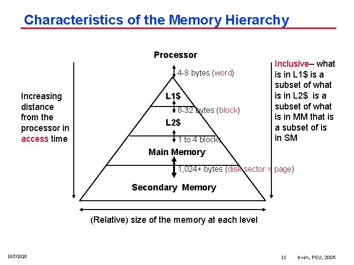
Characteristics of the Memory Hierarchy Processor 4 8 bytes (word) Increasing distance from the processor in access time L 1$ 8 32 bytes (block) L 2$ 1 to 4 blocks Inclusive– what is in L 1$ is a subset of what is in L 2$ is a subset of what is in MM that is a subset of is in SM Main Memory 1, 024+ bytes (disk sector = page) Secondary Memory (Relative) size of the memory at each level 10/7/2020 15 Irwin, PSU, 2005

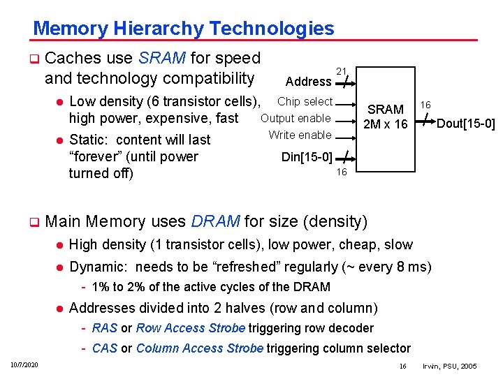
Memory Hierarchy Technologies q Caches use SRAM for speed and technology compatibility l l q Address 21 Low density (6 transistor cells), Chip select Output enable high power, expensive, fast Static: content will last “forever” (until power turned off) SRAM 2 M x 16 Write enable 16 Dout[15 0] Din[15 0] 16 Main Memory uses DRAM for size (density) l High density (1 transistor cells), low power, cheap, slow l Dynamic: needs to be “refreshed” regularly (~ every 8 ms) 1% to 2% of the active cycles of the DRAM l Addresses divided into 2 halves (row and column) RAS or Row Access Strobe triggering row decoder CAS or Column Access Strobe triggering column selector 10/7/2020 16 Irwin, PSU, 2005

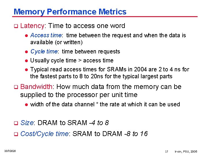
Memory Performance Metrics q q Latency: Time to access one word l Access time: time between the request and when the data is available (or written) l Cycle time: time between requests l Usually cycle time > access time l Typical read access times for SRAMs in 2004 are 2 to 4 ns for the fastest parts to 8 to 20 ns for the typical largest parts Bandwidth: How much data from the memory can be supplied to the processor per unit time l width of the data channel * the rate at which it can be used q Size: DRAM to SRAM 4 to 8 q Cost/Cycle time: SRAM to DRAM 8 to 16 10/7/2020 17 Irwin, PSU, 2005

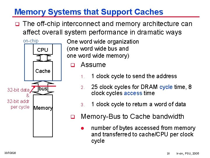
Memory Systems that Support Caches q The off chip interconnect and memory architecture can affect overall system performance in dramatic ways on chip CPU One word wide organization (one word wide bus and one word wide memory) q Cache bus 32 bit data & 32 bit addr per cycle Memory q Assume 1. 1 clock cycle to send the address 2. 25 clock cycles for DRAM cycle time, 8 clock cycles access time 3. 1 clock cycle to return a word of data Memory Bus to Cache bandwidth l 10/7/2020 number of bytes accessed from memory and transferred to cache/CPU per clock cycle 18 Irwin, PSU, 2005

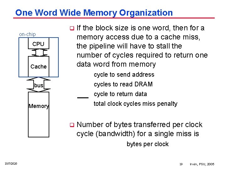
One Word Wide Memory Organization on chip q CPU Cache If the block size is one word, then for a memory access due to a cache miss, the pipeline will have to stall the number of cycles required to return one data word from memory cycle to send address cycles to read DRAM bus cycle to return data total clock cycles miss penalty Memory q Number of bytes transferred per clock cycle (bandwidth) for a single miss is bytes per clock 10/7/2020 19 Irwin, PSU, 2005

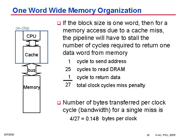
One Word Wide Memory Organization on chip q CPU Cache bus Memory q If the block size is one word, then for a memory access due to a cache miss, the pipeline will have to stall the number of cycles required to return one data word from memory 1 25 1 cycle to send address 27 total clock cycles miss penalty cycles to read DRAM cycle to return data Number of bytes transferred per clock cycle (bandwidth) for a single miss is 4/27 = 0. 148 bytes per clock 10/7/2020 20 Irwin, PSU, 2005

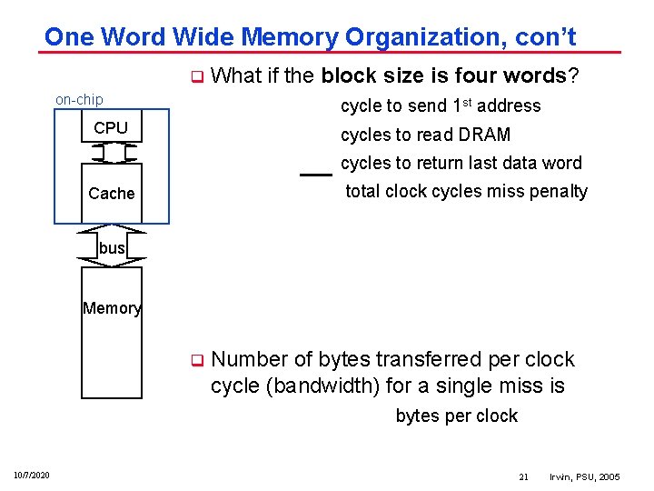
One Word Wide Memory Organization, con’t q on chip What if the block size is four words? cycle to send 1 st address CPU cycles to read DRAM cycles to return last data word total clock cycles miss penalty Cache bus Memory q Number of bytes transferred per clock cycle (bandwidth) for a single miss is bytes per clock 10/7/2020 21 Irwin, PSU, 2005

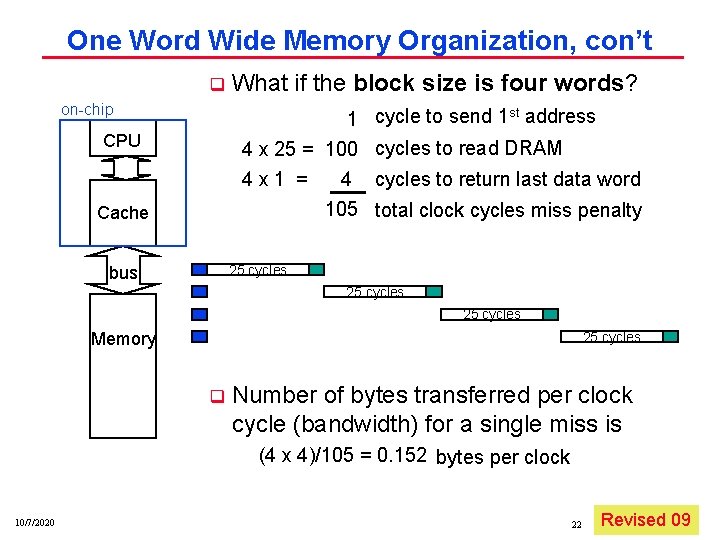
One Word Wide Memory Organization, con’t q on chip What if the block size is four words? 1 cycle to send 1 st address 4 x 25 = 100 cycles to read DRAM 4 x 1 = 4 cycles to return last data word CPU 105 total clock cycles miss penalty Cache 25 cycles bus 25 cycles Memory 25 cycles q Number of bytes transferred per clock cycle (bandwidth) for a single miss is (4 x 4)/105 = 0. 152 bytes per clock 10/7/2020 22 Revised 09 Irwin, PSU, 2005

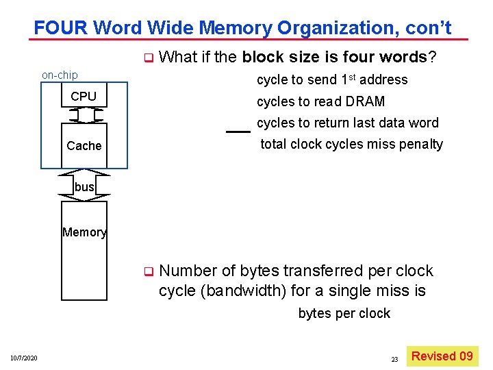
FOUR Word Wide Memory Organization, con’t q on chip What if the block size is four words? cycle to send 1 st address CPU cycles to read DRAM cycles to return last data word total clock cycles miss penalty Cache bus Memory q Number of bytes transferred per clock cycle (bandwidth) for a single miss is bytes per clock 10/7/2020 23 Revised 09 Irwin, PSU, 2005

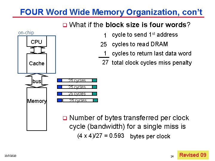
FOUR Word Wide Memory Organization, con’t q What if the block size is four words? on chip 1 cycle to send 1 st address 25 cycles to read DRAM CPU 1 cycles to return last data word 27 total clock cycles miss penalty Cache 25 cycles bus 25 cycles Memory 25 cycles q Number of bytes transferred per clock cycle (bandwidth) for a single miss is (4 x 4)/27 = 0. 593 10/7/2020 bytes per clock 24 Revised 09 Irwin, PSU, 2005

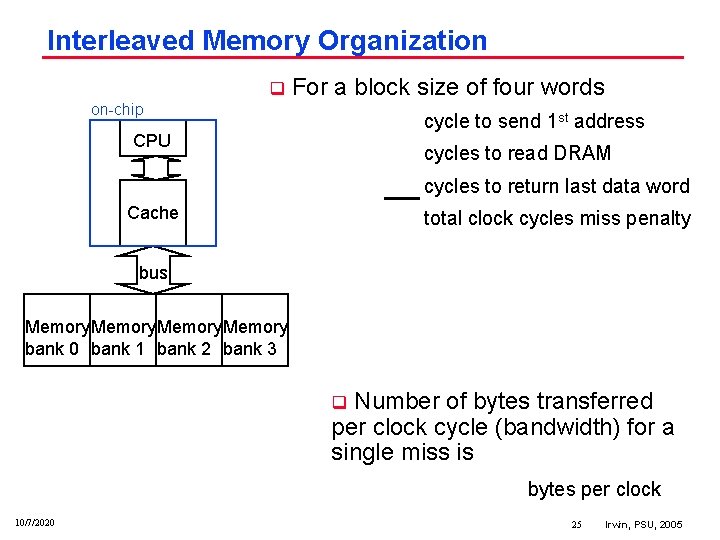
Interleaved Memory Organization q For a block size of four words on chip cycle to send 1 st address CPU cycles to read DRAM cycles to return last data word Cache total clock cycles miss penalty bus Memory bank 0 bank 1 bank 2 bank 3 Number of bytes transferred per clock cycle (bandwidth) for a single miss is q bytes per clock 10/7/2020 25 Irwin, PSU, 2005

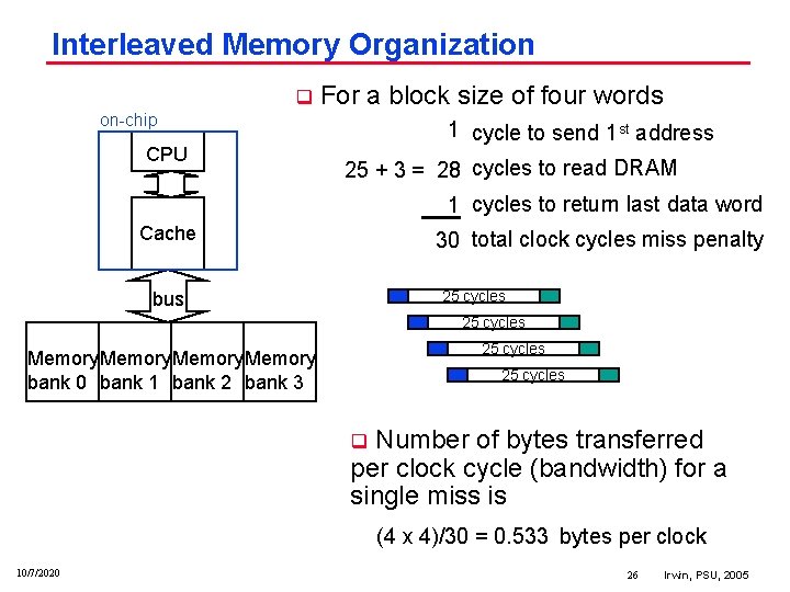
Interleaved Memory Organization q For a block size of four words on chip CPU 1 cycle to send 1 st address 25 + 3 = 28 cycles to read DRAM 1 cycles to return last data word Cache 30 total clock cycles miss penalty 25 cycles bus 25 cycles Memory bank 0 bank 1 bank 2 bank 3 25 cycles Number of bytes transferred per clock cycle (bandwidth) for a single miss is q (4 x 4)/30 = 0. 533 bytes per clock 10/7/2020 26 Irwin, PSU, 2005

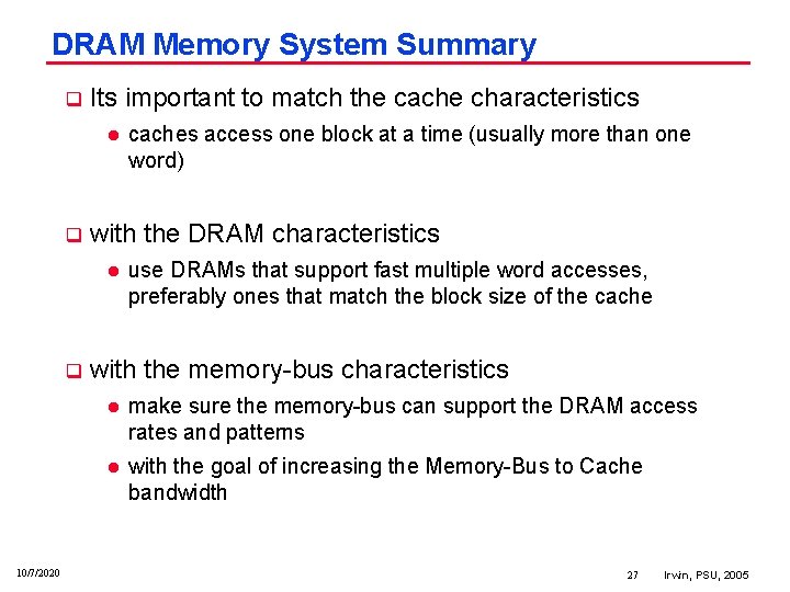
DRAM Memory System Summary q Its important to match the cache characteristics l q with the DRAM characteristics l q 10/7/2020 caches access one block at a time (usually more than one word) use DRAMs that support fast multiple word accesses, preferably ones that match the block size of the cache with the memory bus characteristics l make sure the memory bus can support the DRAM access rates and patterns l with the goal of increasing the Memory Bus to Cache bandwidth 27 Irwin, PSU, 2005

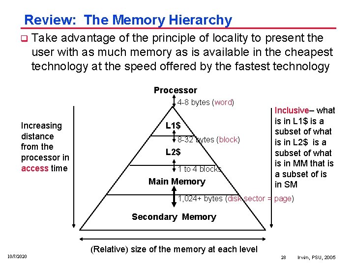
Review: The Memory Hierarchy q Take advantage of the principle of locality to present the user with as much memory as is available in the cheapest technology at the speed offered by the fastest technology Processor 4 8 bytes (word) Increasing distance from the processor in access time L 1$ 8 32 bytes (block) L 2$ 1 to 4 blocks Main Memory Inclusive– what is in L 1$ is a subset of what is in L 2$ is a subset of what is in MM that is a subset of is in SM 1, 024+ bytes (disk sector = page) Secondary Memory 10/7/2020 (Relative) size of the memory at each level 28 Irwin, PSU, 2005

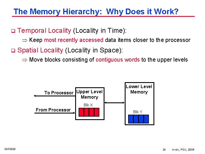
The Memory Hierarchy: Why Does it Work? q Temporal Locality (Locality in Time): Keep most recently accessed data items closer to the processor q Spatial Locality (Locality in Space): Move blocks consisting of contiguous words to the upper levels To Processor Upper Level Memory Lower Level Memory Blk X From Processor 10/7/2020 Blk Y 29 Irwin, PSU, 2005

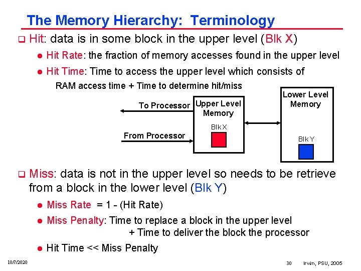
The Memory Hierarchy: Terminology q Hit: data is in some block in the upper level (Blk X) l Hit Rate: the fraction of memory accesses found in the upper level l Hit Time: Time to access the upper level which consists of RAM access time + Time to determine hit/miss To Processor Upper Level Memory Lower Level Memory Blk X From Processor q 10/7/2020 Blk Y Miss: data is not in the upper level so needs to be retrieve from a block in the lower level (Blk Y) l Miss Rate = 1 (Hit Rate) l Miss Penalty: Time to replace a block in the upper level + Time to deliver the block the processor l Hit Time << Miss Penalty 30 Irwin, PSU, 2005

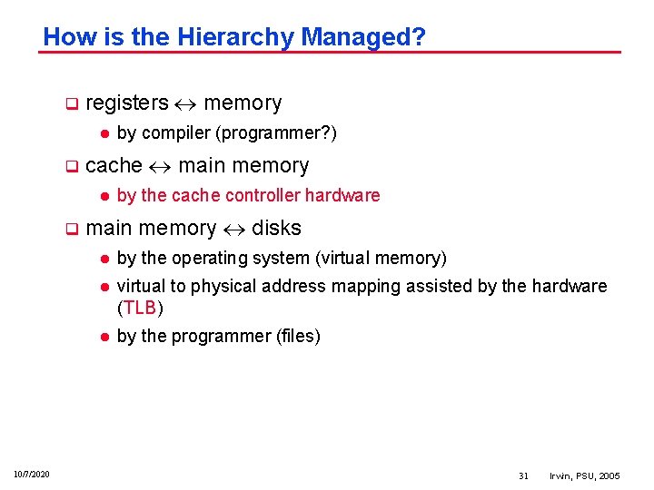
How is the Hierarchy Managed? q registers memory l q cache main memory l q 10/7/2020 by compiler (programmer? ) by the cache controller hardware main memory disks l by the operating system (virtual memory) l virtual to physical address mapping assisted by the hardware (TLB) l by the programmer (files) 31 Irwin, PSU, 2005

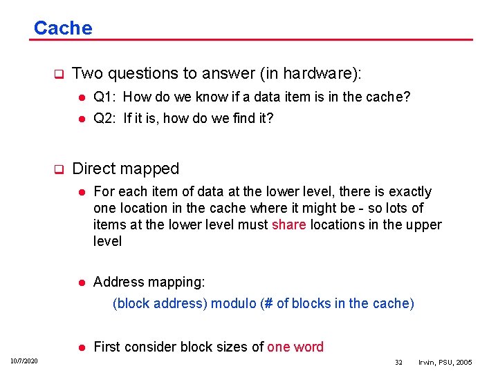
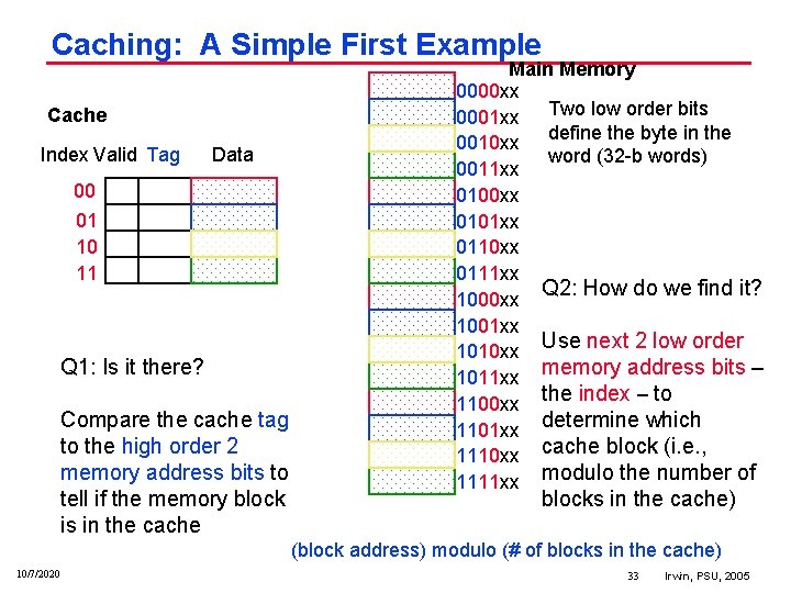
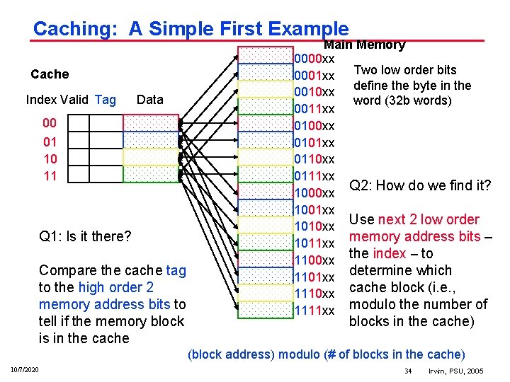
Cache q q Two questions to answer (in hardware): l Q 1: How do we know if a data item is in the cache? l Q 2: If it is, how do we find it? Direct mapped l For each item of data at the lower level, there is exactly one location in the cache where it might be so lots of items at the lower level must share locations in the upper level l Address mapping: (block address) modulo (# of blocks in the cache) l 10/7/2020 First consider block sizes of one word 32 Irwin, PSU, 2005

Caching: A Simple First Example Cache Index Valid Tag Data 00 01 10 11 Q 1: Is it there? Compare the cache tag to the high order 2 memory address bits to tell if the memory block is in the cache Main Memory 0000 xx 0001 xx Two low order bits define the byte in the 0010 xx word (32 b words) 0011 xx 0100 xx 0101 xx 0110 xx 0111 xx Q 2: How do we find it? 1000 xx 1001 xx Use next 2 low order 1010 xx memory address bits – 1011 xx 1100 xx the index – to 1101 xx determine which 1110 xx cache block (i. e. , 1111 xx modulo the number of blocks in the cache) (block address) modulo (# of blocks in the cache) 10/7/2020 33 Irwin, PSU, 2005

Caching: A Simple First Example Cache Index Valid Tag Data 00 01 10 11 Q 1: Is it there? Compare the cache tag to the high order 2 memory address bits to tell if the memory block is in the cache Main Memory 0000 xx 0001 xx Two low order bits define the byte in the 0010 xx word (32 b words) 0011 xx 0100 xx 0101 xx 0110 xx 0111 xx Q 2: How do we find it? 1000 xx 1001 xx Use next 2 low order 1010 xx memory address bits – 1011 xx 1100 xx the index – to 1101 xx determine which 1110 xx cache block (i. e. , 1111 xx modulo the number of blocks in the cache) (block address) modulo (# of blocks in the cache) 10/7/2020 34 Irwin, PSU, 2005

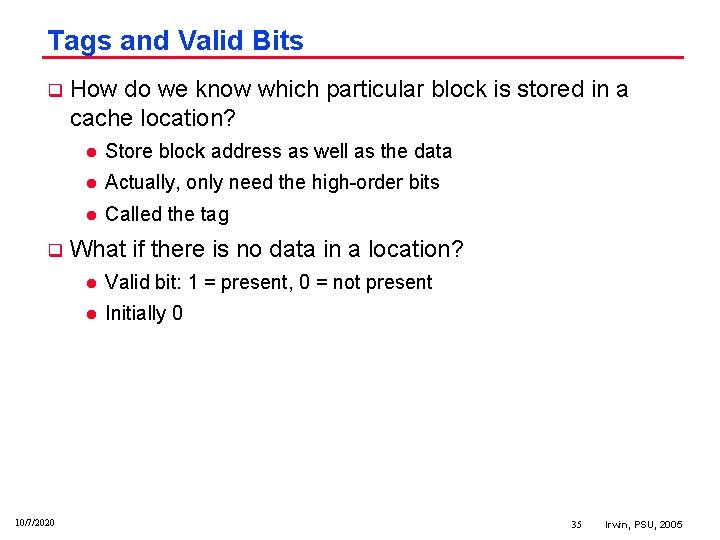
Tags and Valid Bits q q 10/7/2020 How do we know which particular block is stored in a cache location? l Store block address as well as the data l Actually, only need the high order bits l Called the tag What if there is no data in a location? l Valid bit: 1 = present, 0 = not present l Initially 0 35 Irwin, PSU, 2005

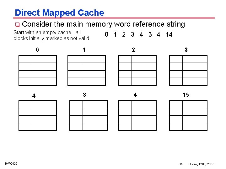
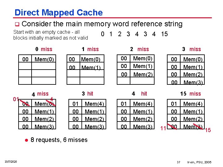
Direct Mapped Cache q Consider the main memory word reference string Start with an empty cache all blocks initially marked as not valid 0 4 10/7/2020 1 3 0 1 2 3 4 14 2 4 3 15 36 Irwin, PSU, 2005

Direct Mapped Cache q Consider the main memory word reference string Start with an empty cache all blocks initially marked as not valid 0 miss 00 01 1 miss 00 Mem(0) 00 Mem(1) 4 miss 00 00 l 10/7/2020 Mem(0) 4 Mem(0) Mem(1) Mem(2) Mem(3) 0 1 2 3 4 15 2 miss 00 00 00 3 hit 01 00 00 00 Mem(4) Mem(1) Mem(2) Mem(3) Mem(0) Mem(1) Mem(2) 4 01 00 00 00 3 miss 00 00 hit Mem(4) Mem(1) Mem(2) Mem(3) Mem(0) Mem(1) Mem(2) Mem(3) 15 miss 01 00 00 11 00 Mem(4) Mem(1) Mem(2) Mem(3) 15 8 requests, 6 misses 37 Irwin, PSU, 2005

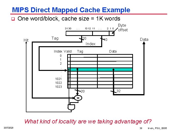
MIPS Direct Mapped Cache Example q One word/block, cache size = 1 K words 31 30 Hit Tag . . . 13 12 11 20 . . . 2 1 0 Byte offset Data 10 Index Valid Tag Data 0 1 2. . . 1021 1022 1023 20 32 What kind of locality are we taking advantage of? 10/7/2020 38 Irwin, PSU, 2005

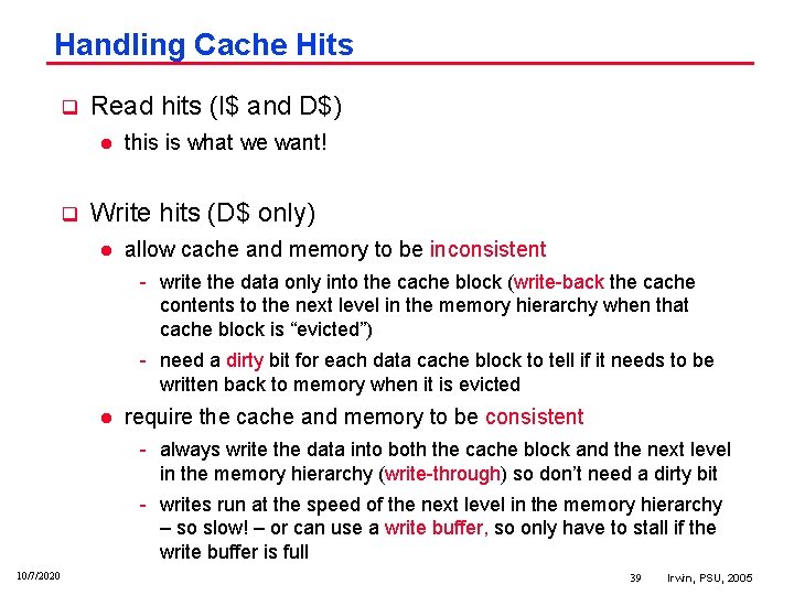
Handling Cache Hits q Read hits (I$ and D$) l q this is what we want! Write hits (D$ only) l allow cache and memory to be inconsistent write the data only into the cache block (write back the cache contents to the next level in the memory hierarchy when that cache block is “evicted”) need a dirty bit for each data cache block to tell if it needs to be written back to memory when it is evicted l require the cache and memory to be consistent always write the data into both the cache block and the next level in the memory hierarchy (write through) so don’t need a dirty bit writes run at the speed of the next level in the memory hierarchy – so slow! – or can use a write buffer, so only have to stall if the write buffer is full 10/7/2020 39 Irwin, PSU, 2005

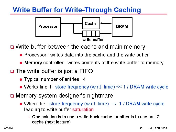
Write Buffer for Write-Through Caching Processor Cache DRAM write buffer q q q Write buffer between the cache and main memory l Processor: writes data into the cache and the write buffer l Memory controller: writes contents of the write buffer to memory The write buffer is just a FIFO l Typical number of entries: 4 l Works fine if store frequency (w. r. t. time) << 1 / DRAM write cycle Memory system designer’s nightmare l When the store frequency (w. r. t. time) → 1 / DRAM write cycle leading to write buffer saturation One solution is to use a write back cache; another is to use an L 2 cache (next lecture) 10/7/2020 40 Irwin, PSU, 2005

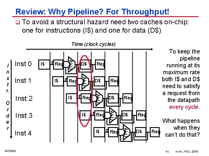
Review: Why Pipeline? For Throughput! q To avoid a structural hazard need two caches on chip: one for instructions (I$) and one for data (D$) Time (clock cycles) Inst 4 10/7/2020 I$ Reg D$ Reg ALU Inst 3 D$ ALU Inst 2 Reg ALU Inst 1 I$ ALU O r d e r Inst 0 ALU I n s t r. To keep the pipeline running at its maximum rate both I$ and D$ need to satisfy a request from the datapath every cycle. Reg I$ Reg Reg D$ Reg What happens when they can’t do that? 41 Irwin, PSU, 2005

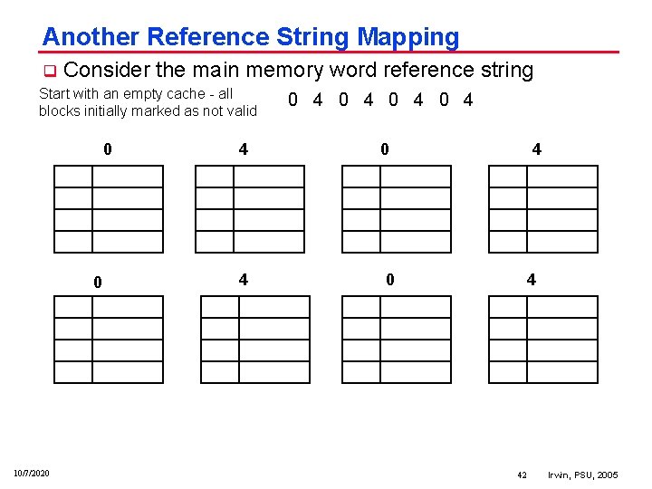
Another Reference String Mapping q Consider the main memory word reference string Start with an empty cache all blocks initially marked as not valid 0 0 10/7/2020 4 4 0 4 0 4 0 0 4 4 42 Irwin, PSU, 2005

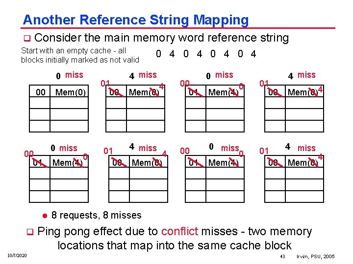
Another Reference String Mapping q Consider the main memory word reference string Start with an empty cache all blocks initially marked as not valid 0 miss 00 00 01 l q 10/7/2020 Mem(0) 0 miss Mem(4) 0 01 00 0 4 0 4 4 miss Mem(0) 4 00 01 0 miss 0 01 00 0 miss 0 Mem(4) 01 00 Mem(4) 4 miss Mem(0)4 4 miss Mem(0) 4 8 requests, 8 misses Ping pong effect due to conflict misses two memory locations that map into the same cache block 43 Irwin, PSU, 2005

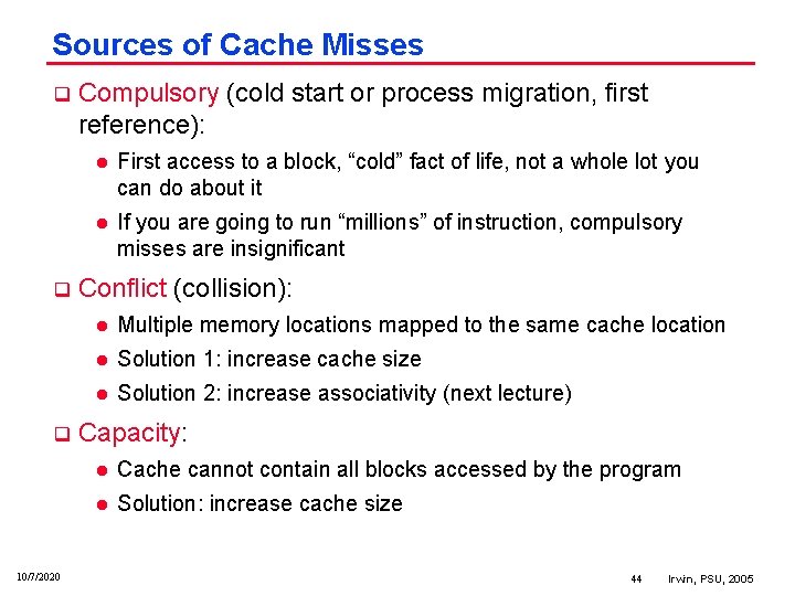
Sources of Cache Misses q q q 10/7/2020 Compulsory (cold start or process migration, first reference): l First access to a block, “cold” fact of life, not a whole lot you can do about it l If you are going to run “millions” of instruction, compulsory misses are insignificant Conflict (collision): l Multiple memory locations mapped to the same cache location l Solution 1: increase cache size l Solution 2: increase associativity (next lecture) Capacity: l Cache cannot contain all blocks accessed by the program l Solution: increase cache size 44 Irwin, PSU, 2005

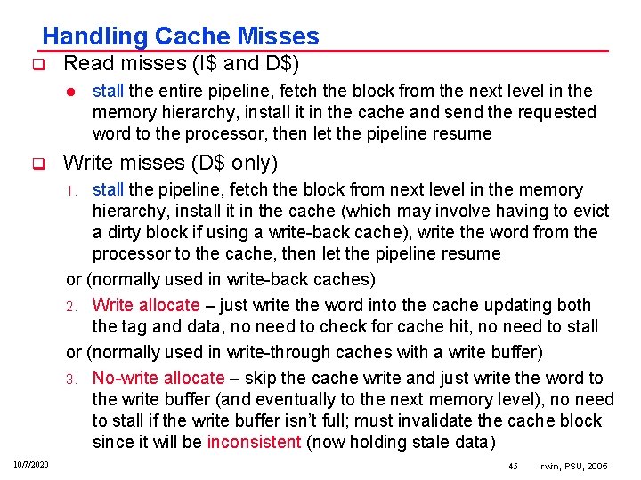
Handling Cache Misses q Read misses (I$ and D$) l q stall the entire pipeline, fetch the block from the next level in the memory hierarchy, install it in the cache and send the requested word to the processor, then let the pipeline resume Write misses (D$ only) stall the pipeline, fetch the block from next level in the memory hierarchy, install it in the cache (which may involve having to evict a dirty block if using a write back cache), write the word from the processor to the cache, then let the pipeline resume or (normally used in write back caches) 2. Write allocate – just write the word into the cache updating both the tag and data, no need to check for cache hit, no need to stall or (normally used in write through caches with a write buffer) 3. No write allocate – skip the cache write and just write the word to the write buffer (and eventually to the next memory level), no need to stall if the write buffer isn’t full; must invalidate the cache block since it will be inconsistent (now holding stale data) 1. 10/7/2020 45 Irwin, PSU, 2005

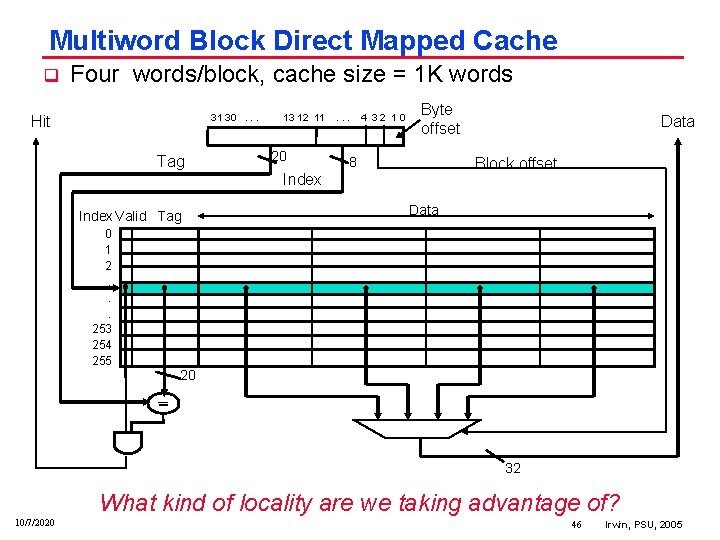
Multiword Block Direct Mapped Cache q Four words/block, cache size = 1 K words 31 30. . . Hit Tag 13 12 11 20 . . . 4 32 10 Byte offset 8 Block offset Index Valid Tag 0 1 2. . . 253 254 255 Data 20 32 What kind of locality are we taking advantage of? 10/7/2020 46 Irwin, PSU, 2005

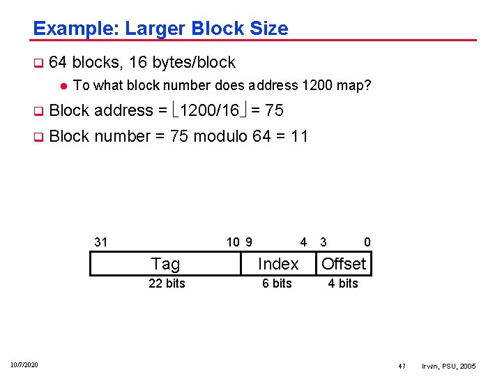
Example: Larger Block Size q 64 blocks, 16 bytes/block l To what block number does address 1200 map? q Block address = 1200/16 = 75 q Block number = 75 modulo 64 = 11 31 10/7/2020 10 9 4 3 0 Tag Index Offset 22 bits 6 bits 47 Irwin, PSU, 2005

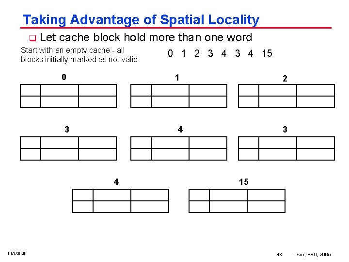
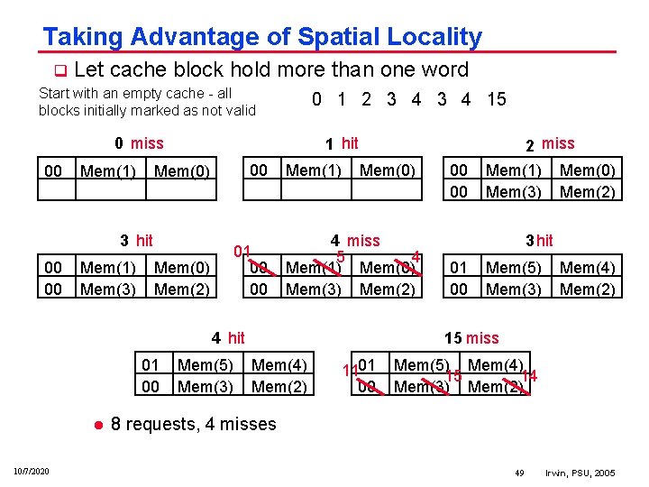
Taking Advantage of Spatial Locality q Let cache block hold more than one word Start with an empty cache all blocks initially marked as not valid 0 1 3 2 4 4 10/7/2020 0 1 2 3 4 15 3 15 48 Irwin, PSU, 2005

Taking Advantage of Spatial Locality q Let cache block hold more than one word Start with an empty cache all blocks initially marked as not valid 0 1 2 3 4 15 0 miss 00 Mem(1) 1 hit Mem(0) 00 Mem(0) Mem(2) 01 00 00 3 hit 00 00 Mem(1) Mem(3) Mem(1) Mem(0) 4 miss 5 4 Mem(1) Mem(0) Mem(3) Mem(2) 4 hit 01 00 l 10/7/2020 Mem(5) Mem(3) 00 00 2 miss Mem(1) Mem(0) Mem(3) Mem(2) 3 hit 01 00 Mem(5) Mem(3) Mem(4) Mem(2) 15 miss Mem(4) Mem(2) 1101 00 Mem(5) Mem(4) 15 14 Mem(3) Mem(2) 8 requests, 4 misses 49 Irwin, PSU, 2005

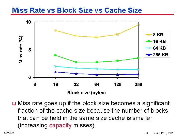
Miss Rate vs Block Size vs Cache Size q 10/7/2020 Miss rate goes up if the block size becomes a significant fraction of the cache size because the number of blocks that can be held in the same size cache is smaller (increasing capacity misses) 50 Irwin, PSU, 2005

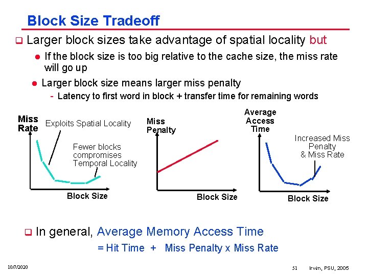
Block Size Tradeoff q Larger block sizes take advantage of spatial locality but l l If the block size is too big relative to the cache size, the miss rate will go up Larger block size means larger miss penalty Latency to first word in block + transfer time for remaining words Miss Exploits Spatial Locality Rate Average Access Time Miss Penalty Increased Miss Penalty & Miss Rate Fewer blocks compromises Temporal Locality Block Size q Block Size In general, Average Memory Access Time = Hit Time + Miss Penalty x Miss Rate 10/7/2020 51 Irwin, PSU, 2005

Multiword Block Considerations q Read misses (I$ and D$) l Processed the same as for single word blocks – a miss returns the entire block from memory l Miss penalty grows as block size grows Early restart – datapath resumes execution as soon as the requested word of the block is returned Requested word first – requested word is transferred from the memory to the cache (and datapath) first l q Write misses (D$) l 10/7/2020 Nonblocking cache – allows the datapath to continue to access the cache while the cache is handling an earlier miss Can’t use write allocate or will end up with a “garbled” block in the cache (e. g. , for 4 word blocks, a new tag, one word of data from the new block, and three words of data from the old block), so must fetch the block from memory first and pay the stall time 52 Irwin, PSU, 2005

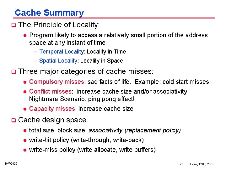
Cache Summary q The Principle of Locality: l Program likely to access a relatively small portion of the address space at any instant of time Temporal Locality: Locality in Time Spatial Locality: Locality in Space q q 10/7/2020 Three major categories of cache misses: l Compulsory misses: sad facts of life. Example: cold start misses l Conflict misses: increase cache size and/or associativity Nightmare Scenario: ping pong effect! l Capacity misses: increase cache size Cache design space l total size, block size, associativity (replacement policy) l write hit policy (write through, write back) l write miss policy (write allocate, write buffers) 53 Irwin, PSU, 2005

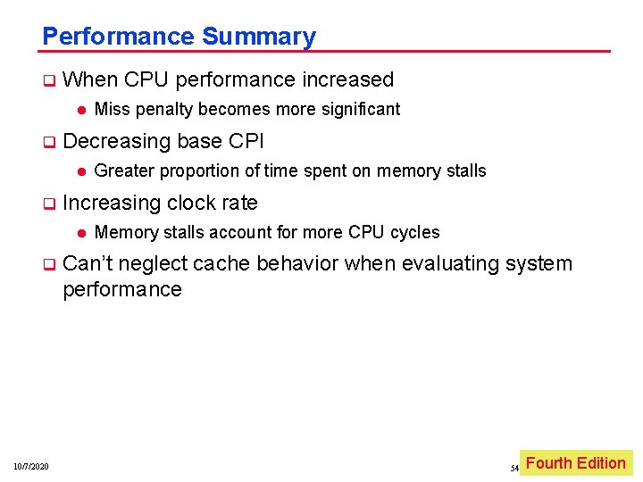
Performance Summary q When CPU performance increased l q Decreasing base CPI l q 10/7/2020 Greater proportion of time spent on memory stalls Increasing clock rate l q Miss penalty becomes more significant Memory stalls account for more CPU cycles Can’t neglect cache behavior when evaluating system performance 54 Fourth Edition Irwin, PSU, 2005

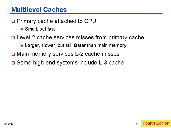
Multilevel Caches q Primary cache attached to CPU l q Small, but fast Level 2 cache services misses from primary cache l Larger, slower, but still faster than main memory q Main memory services L 2 cache misses q Some high end systems include L 3 cache 10/7/2020 55 Fourth Irwin, PSU, Edition 2005

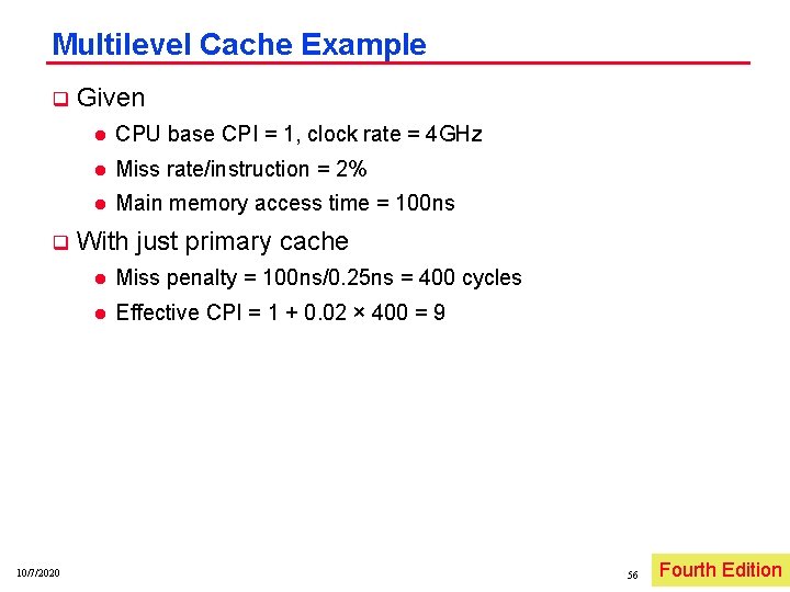
Multilevel Cache Example q q 10/7/2020 Given l CPU base CPI = 1, clock rate = 4 GHz l Miss rate/instruction = 2% l Main memory access time = 100 ns With just primary cache l Miss penalty = 100 ns/0. 25 ns = 400 cycles l Effective CPI = 1 + 0. 02 × 400 = 9 56 Fourth Irwin, PSU, Edition 2005

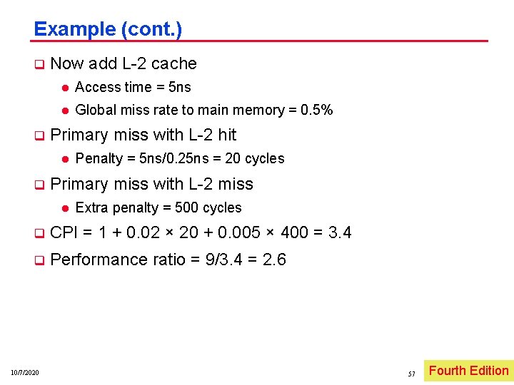
Example (cont. ) q q Now add L 2 cache l Access time = 5 ns l Global miss rate to main memory = 0. 5% Primary miss with L 2 hit l q Penalty = 5 ns/0. 25 ns = 20 cycles Primary miss with L 2 miss l Extra penalty = 500 cycles q CPI = 1 + 0. 02 × 20 + 0. 005 × 400 = 3. 4 q Performance ratio = 9/3. 4 = 2. 6 10/7/2020 57 Fourth Irwin, PSU, Edition 2005

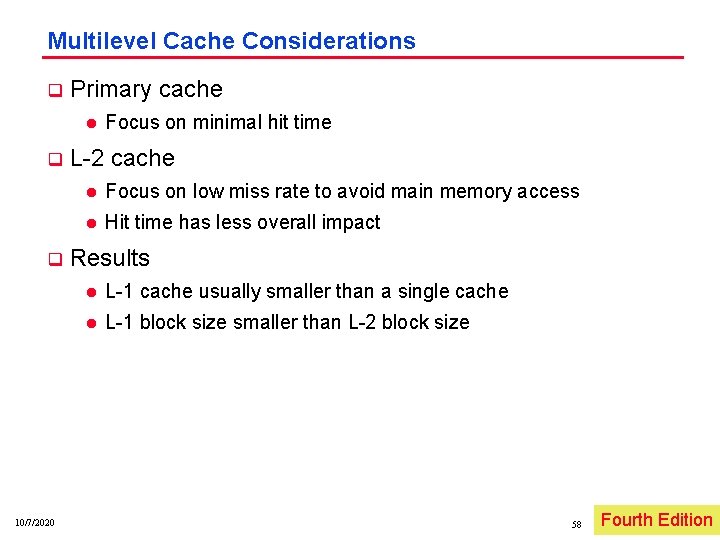
Multilevel Cache Considerations q Primary cache l q q 10/7/2020 Focus on minimal hit time L 2 cache l Focus on low miss rate to avoid main memory access l Hit time has less overall impact Results l L 1 cache usually smaller than a single cache l L 1 block size smaller than L 2 block size 58 Fourth Irwin, PSU, Edition 2005

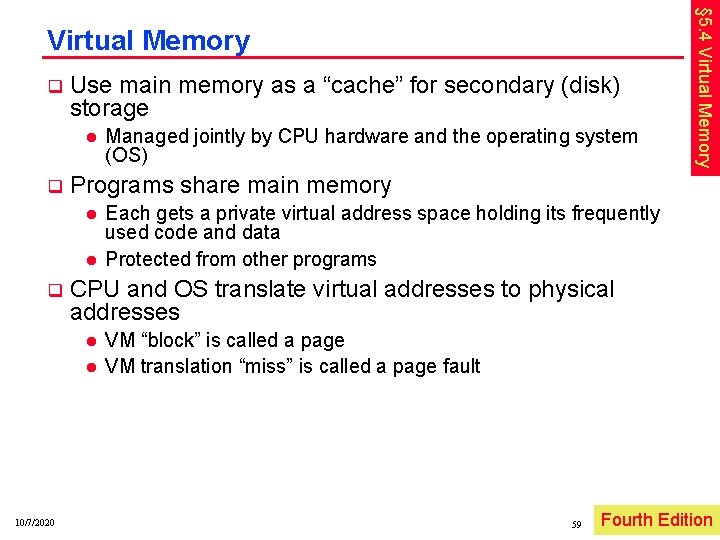
q Use main memory as a “cache” for secondary (disk) storage l q Programs share main memory l l q Each gets a private virtual address space holding its frequently used code and data Protected from other programs CPU and OS translate virtual addresses to physical addresses l l 10/7/2020 Managed jointly by CPU hardware and the operating system (OS) § 5. 4 Virtual Memory VM “block” is called a page VM translation “miss” is called a page fault 59 Fourth Irwin, PSU, Edition 2005

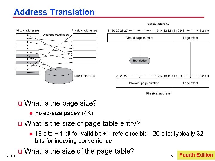
Address Translation q What is the page size? l q What is the size of page table entry? l 10/7/2020 q Fixed size pages (4 K) 18 bits + 1 bit for valid bit + 1 reference bit = 20 bits; typically 32 bits for indexing convenience What is the size of the page table? 60 Fourth Irwin, PSU, Edition 2005

Page Table Size q Typical Parameters: 32 bit virtual address; 4 KB pages; 4 bytes per page table entry q Number of PTEs = virtual address space / page size = 232/212 = 220 q Size of page table = 220 PTEs X 4 bytes/PTE = 2 22 bytes = 4 MB q q 10/7/2020 Each program has its own page table. So if 1000 programs are running then all page tables will use 4 GB of main memory. Approaches to limit page table l Most programs do not use entire virtual space. Use a limit register to restrict size – if a user goes above limit then increase page table size. l Store pages on disk – sort of like virtual memory. 61 Irwin, PSU, 2005

Page Fault Penalty q q 10/7/2020 On page fault, the page must be fetched from disk l Takes millions of clock cycles l Handled by OS code Try to minimize page fault rate l Fully associative placement l Smart replacement algorithms 62 Fourth Irwin, PSU, Edition 2005

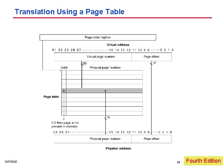
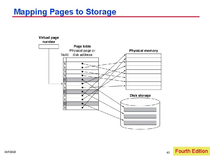
Page Tables q Stores placement information l l q If page is present in memory l l q PTE stores the physical page number Plus other status bits (referenced, dirty, …) If page is not present l 10/7/2020 Array of page table entries, indexed by virtual page number Page table register in CPU points to page table in physical memory PTE can refer to location in swap space on disk 63 Fourth Irwin, PSU, Edition 2005

Translation Using a Page Table 10/7/2020 64 Fourth Irwin, PSU, Edition 2005

Mapping Pages to Storage 10/7/2020 65 Fourth Irwin, PSU, Edition 2005

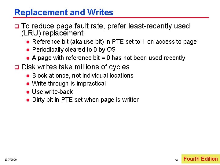
Replacement and Writes q To reduce page fault rate, prefer least recently used (LRU) replacement l l l q Disk writes take millions of cycles l l 10/7/2020 Reference bit (aka use bit) in PTE set to 1 on access to page Periodically cleared to 0 by OS A page with reference bit = 0 has not been used recently Block at once, not individual locations Write through is impractical Use write back Dirty bit in PTE set when page is written 66 Fourth Irwin, PSU, Edition 2005

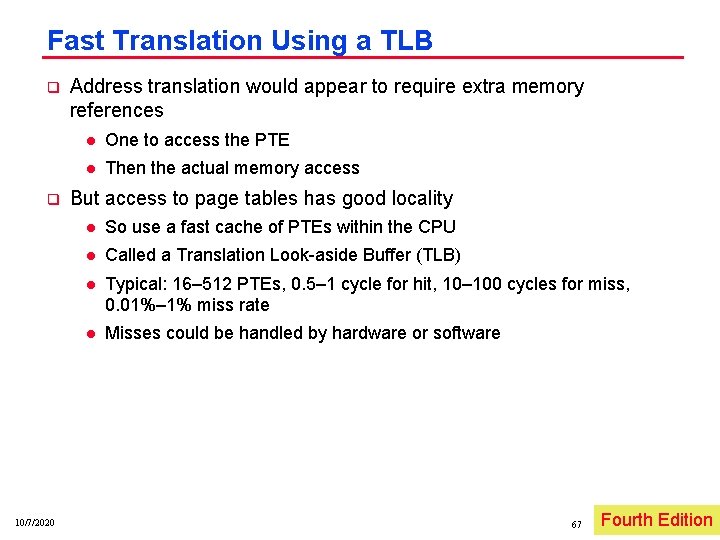
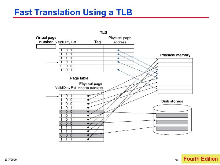
Fast Translation Using a TLB q q 10/7/2020 Address translation would appear to require extra memory references l One to access the PTE l Then the actual memory access But access to page tables has good locality l So use a fast cache of PTEs within the CPU l Called a Translation Look aside Buffer (TLB) l Typical: 16– 512 PTEs, 0. 5– 1 cycle for hit, 10– 100 cycles for miss, 0. 01%– 1% miss rate l Misses could be handled by hardware or software 67 Fourth Irwin, PSU, Edition 2005

Fast Translation Using a TLB 10/7/2020 68 Fourth Irwin, PSU, Edition 2005

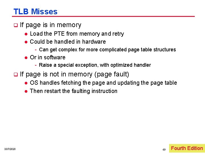
TLB Misses q If page is in memory l l Load the PTE from memory and retry Could be handled in hardware Can get complex for more complicated page table structures l Or in software Raise a special exception, with optimized handler q If page is not in memory (page fault) l l 10/7/2020 OS handles fetching the page and updating the page table Then restart the faulting instruction 69 Fourth Irwin, PSU, Edition 2005

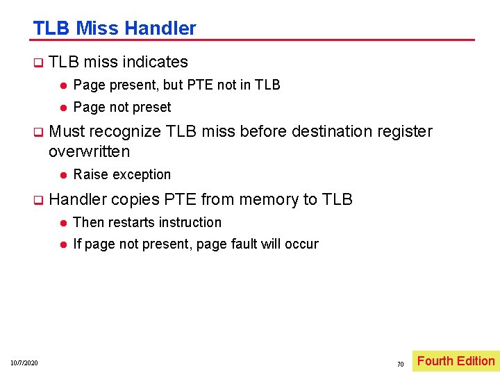
TLB Miss Handler q q TLB miss indicates l Page present, but PTE not in TLB l Page not preset Must recognize TLB miss before destination register overwritten l q 10/7/2020 Raise exception Handler copies PTE from memory to TLB l Then restarts instruction l If page not present, page fault will occur 70 Fourth Irwin, PSU, Edition 2005

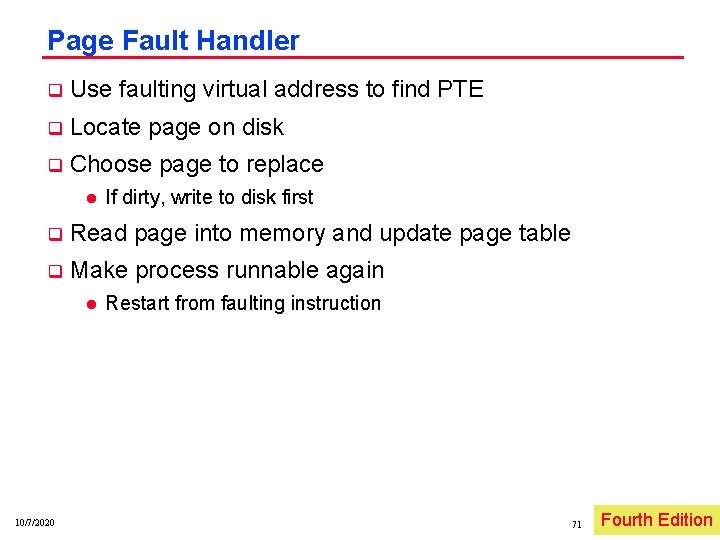
Page Fault Handler q Use faulting virtual address to find PTE q Locate page on disk q Choose page to replace l If dirty, write to disk first q Read page into memory and update page table q Make process runnable again l 10/7/2020 Restart from faulting instruction 71 Fourth Irwin, PSU, Edition 2005

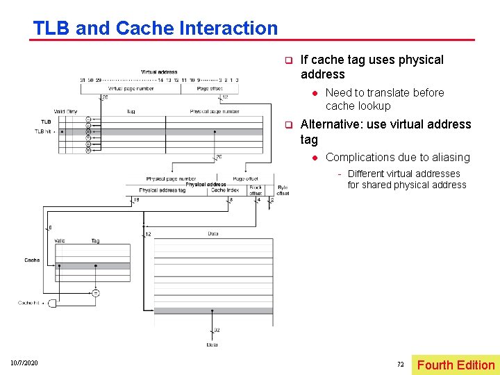
TLB and Cache Interaction q If cache tag uses physical address l q Need to translate before cache lookup Alternative: use virtual address tag l Complications due to aliasing Different virtual addresses for shared physical address 10/7/2020 72 Irwin, PSU, Edition 2005 Fourth

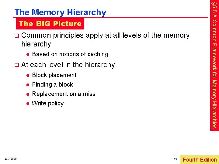
The BIG Picture q Common principles apply at all levels of the memory hierarchy l q 10/7/2020 Based on notions of caching At each level in the hierarchy l Block placement l Finding a block l Replacement on a miss l Write policy 73 § 5. 5 A Common Framework for Memory Hierarchies The Memory Hierarchy Irwin, PSU, Edition 2005 Fourth

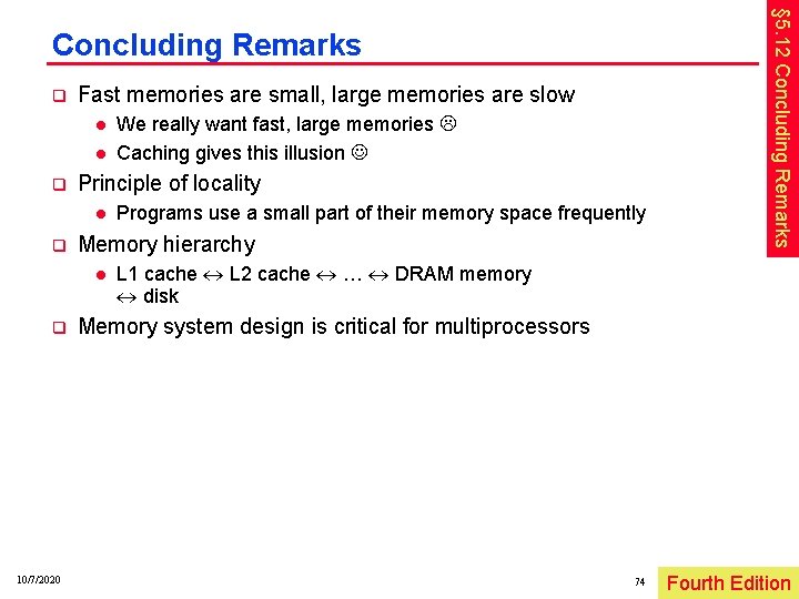
q Fast memories are small, large memories are slow l l q Principle of locality l q 10/7/2020 Programs use a small part of their memory space frequently Memory hierarchy l q We really want fast, large memories Caching gives this illusion § 5. 12 Concluding Remarks L 1 cache L 2 cache … DRAM memory disk Memory system design is critical for multiprocessors 74 Irwin, PSU, Edition 2005 Fourth