Memory Management Units for Instruction and Data Cache






- Slides: 20

Memory Management Units for Instruction and Data Cache for OR 1200 CPU Core st Robu Low Robust er Pow LSI V Power VLSI Arijit Banerjee Dated 05/09/2014 ASIC/SOC Class 2014

Motivation § ASICs/So. Cs have billions of transistors § Impossible to design everything manually st Robu Low er Pow VLSI § Cad tools to the rescue § To learn the basic full cad flow for ASIC/So. C design § MMU hard IP design as part of full processor design project 2

Overview of Memory Management Unit § Memory Management Unit (MMU) an essential module in modern processors § Manages translation of virtual (logical) memory address space to physical address space § Provides memory protection for software programs st Robu Low er Pow VLSI Source : http: //en. wikipedia. org/wiki/File: MMU_principle_updated. png 3

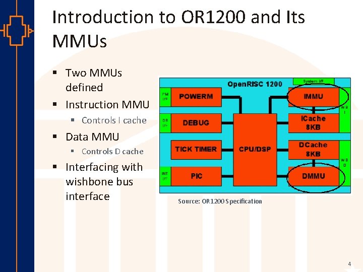
Introduction to OR 1200 and Its MMUs § Two MMUs defined § Instruction MMU § Controls I cache § Data MMU § Controls D cache § Interfacing with wishbone bus interface Source: OR 1200 Specification st Robu Low er Pow VLSI 4

MMU Address translation Mechanism in OR 1200 MMUs st Robu Low er Pow VLSI § MMU divides the virtual address space into pages § It uses an in-memory table of items called “page table” that contains a “page table entry” (PTE) per page, to map the virtual page numbers to physical memory § PTE has an associative cache called translation lookaside buffer (TLB) to avoid accessing main memory per address translation Source: OR 1200 Specification 5

Basic Cad Flow for MMU Hard IP Design § § Source HDL Modification Synthesis of individual blocks Formal Verification Place and Route st Robu Low er Pow VLSI 6

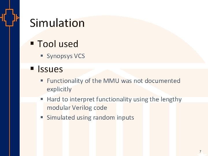
Simulation § Tool used § Synopsys VCS § Issues st Robu Low er Pow VLSI § Functionality of the MMU was not documented explicitly § Hard to interpret functionality using the lengthy modular Verilog code § Simulated using random inputs 7

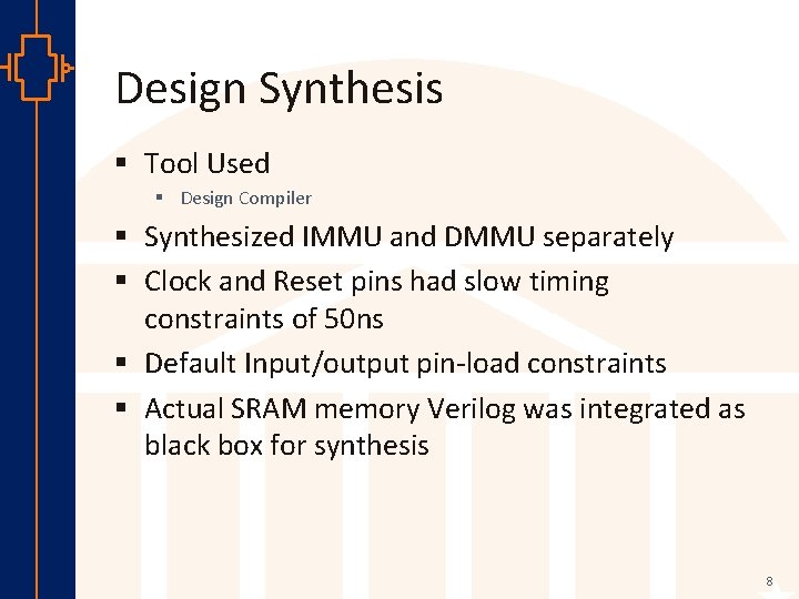
Design Synthesis § Tool Used § Design Compiler st Robu Low er Pow VLSI § Synthesized IMMU and DMMU separately § Clock and Reset pins had slow timing constraints of 50 ns § Default Input/output pin-load constraints § Actual SRAM memory Verilog was integrated as black box for synthesis 8

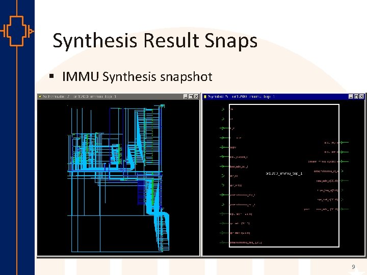
Synthesis Result Snaps § IMMU Synthesis snapshot st Robu Low er Pow VLSI 9

Formal Verification § Tool used § Formality § SRAMs were treated as black boxes in the verification § SRAM Verilog was ports only for comparison § Successfully verified both IMMU and DMMU st Robu Low er Pow VLSI 10

Milkyway Database Preparation for SRAM Hard Macros § Created the Tutorial for SRAM hard macro data base preparation § Method § Create the library and attach the technology file § Import the DEF there after § Issues st Robu Low er Pow VLSI § Directly DEF imports fails due as the DEF does not have technology file information § Verilog and DEF has port mismatch due to SRAM compiler bug for Verilog generation 11

Place and Route § Tools use § IC Compiler (ICC) § Used the SRAM hard macro Milkyway databases § 64 X 14, 64 X 22 and 64 x 24 macros § IMMU need manual floor planning as SRAM macros were overlapping on top of each other st Robu Low er Pow VLSI § Placement of Hard macros were fixed § Placement blockage was placed over the SRAM macros § DMMU uses normal scripted flow 12

ICC Result Snapshots § Before fixing the aspect ratio DMMU and IMMU § 246 X 246 square microns st Robu Low er Pow VLSI 13

ICC Result Snapshots § After fixing the aspect ratio at 1. 318 for DMMU and IMMU § 289 X 220 square microns st Robu Low er Pow VLSI 14

Deliverables § Wiki updated with all the deliverable materials including the Milkyway database creation with SRAM DEFs tutorial § Scripts uploaded in wiki § § st Robu Low er Pow VLSI DVE DC Formality ICC § SRAM Milkyway databases for macros 64 x 14, 64 x 22 and 64 x 24 uploaded in wiki and collab § Full placed and routed macro uploaded in collab dropbox 15

Issues Faced § Had less time to learn the full flow § Skipped the Hercules DRC and LVS for the design § Also skipped Primetime signoff § Place and route using ICC showed following issues those are yet to be resolved § Floating net issues flags errors § VDD and VSS disconnection errors § In some cases, for unknown causes the ICC takes infinitely long time to check “Notch DRCs” st Robu Low er Pow VLSI 16

Conclusion st Robu Low er Pow VLSI § We learned a great deal of information about the full cad flow for ASIC/So. C design § Also learned about the OR 1200 and its DMMUs and in general MMU’s internal working mechanism § Had hands on tools and its flows like VCS, DC, Formality, ICC etc. § Delivered the final Milkyway database for the DMMU and IMMU within the course time § However, had issues with ICC about net connection errors those are yet to debug 17

Future Possibility st Robu Low er Pow VLSI § To start the project earlier after two to three weeks from starting § Collect more information about the ICC flow and Develop a concrete ICC flow that works § Include EMIR in the ICC flow (already made the tutorial ) § Include Hercules DRC and LVS verification for the final layouts § Signoff timing checks using prime time § (Integrate a full project and tapeout) 18

Questions st Robu Low er Pow VLSI 19

Overview contd. § TLB is not mandatory; however it improves address translation speed § A PTE can include information about § § If the page is written When it was last used What process has the PTE associated with Weather or not it should be cached etc. st Robu Low er Pow VLSI 20