Memory Hierarchy Reducing Miss Penalty Reducing Hit Time

![Avoiding Bank Conflicts • Lots of banks int x[256][512]; for (j = 0; j Avoiding Bank Conflicts • Lots of banks int x[256][512]; for (j = 0; j](https://slidetodoc.com/presentation_image/1321bbc33e5db30f8e26e5eda97ca35d/image-29.jpg)
- Slides: 37

Memory Hierarchy— Reducing Miss Penalty Reducing Hit Time Main Memory Professor Alvin R. Lebeck Computer Science 220 / ECE 252 Fall 2006

Admin Work on Projects Read NUCA paper © Alvin R. Lebeck 2006 2

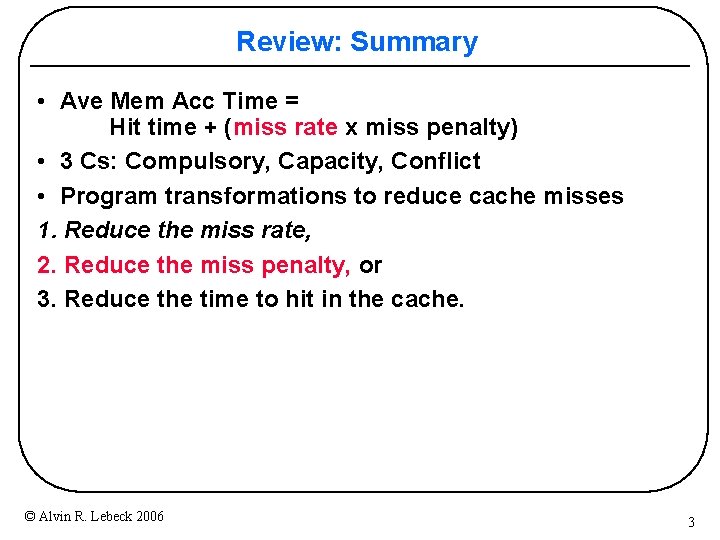
Review: Summary • Ave Mem Acc Time = Hit time + (miss rate x miss penalty) • 3 Cs: Compulsory, Capacity, Conflict • Program transformations to reduce cache misses 1. Reduce the miss rate, 2. Reduce the miss penalty, or 3. Reduce the time to hit in the cache. © Alvin R. Lebeck 2006 3

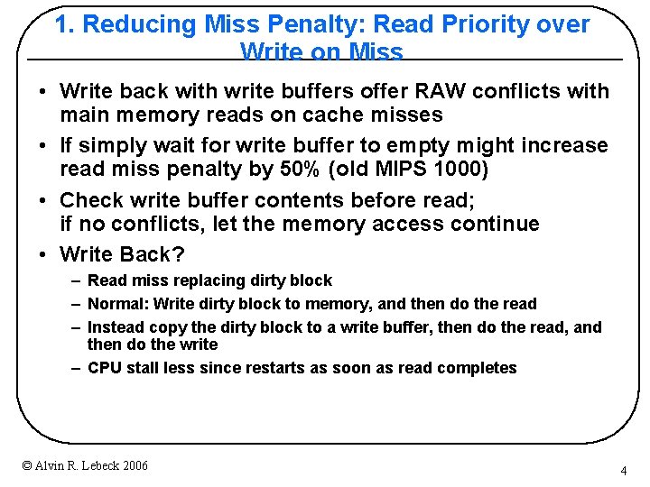
1. Reducing Miss Penalty: Read Priority over Write on Miss • Write back with write buffers offer RAW conflicts with main memory reads on cache misses • If simply wait for write buffer to empty might increase read miss penalty by 50% (old MIPS 1000) • Check write buffer contents before read; if no conflicts, let the memory access continue • Write Back? – Read miss replacing dirty block – Normal: Write dirty block to memory, and then do the read – Instead copy the dirty block to a write buffer, then do the read, and then do the write – CPU stall less since restarts as soon as read completes © Alvin R. Lebeck 2006 4

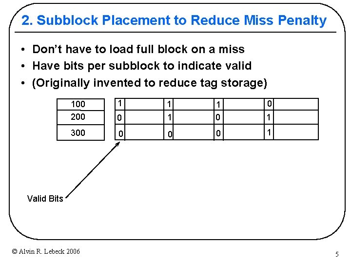
2. Subblock Placement to Reduce Miss Penalty • Don’t have to load full block on a miss • Have bits per subblock to indicate valid • (Originally invented to reduce tag storage) 100 200 300 1 0 0 1 1 1 0 0 0 1 Valid Bits © Alvin R. Lebeck 2006 5

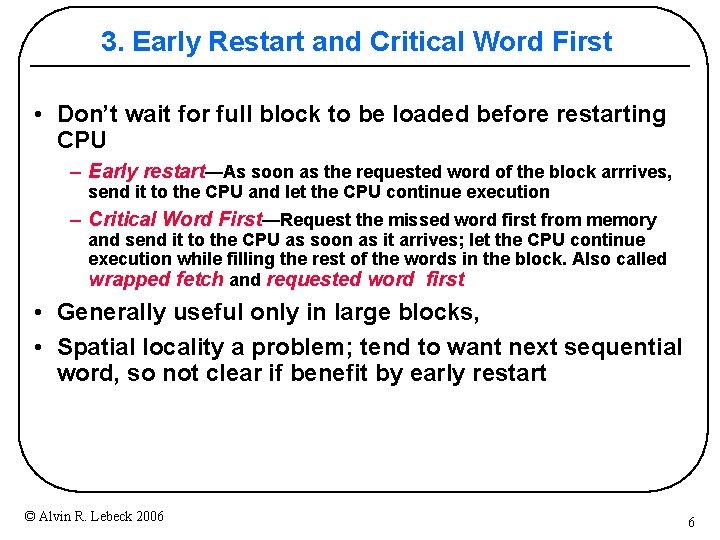
3. Early Restart and Critical Word First • Don’t wait for full block to be loaded before restarting CPU – Early restart—As soon as the requested word of the block arrrives, send it to the CPU and let the CPU continue execution – Critical Word First—Request the missed word first from memory and send it to the CPU as soon as it arrives; let the CPU continue execution while filling the rest of the words in the block. Also called wrapped fetch and requested word first • Generally useful only in large blocks, • Spatial locality a problem; tend to want next sequential word, so not clear if benefit by early restart © Alvin R. Lebeck 2006 6

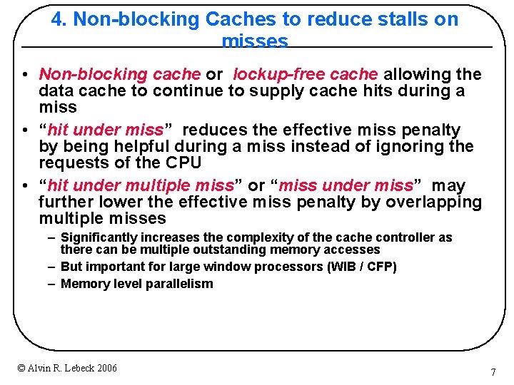
4. Non blocking Caches to reduce stalls on misses • Non-blocking cache or lockup-free cache allowing the data cache to continue to supply cache hits during a miss • “hit under miss” reduces the effective miss penalty by being helpful during a miss instead of ignoring the requests of the CPU • “hit under multiple miss” or “miss under miss” may further lower the effective miss penalty by overlapping multiple misses – Significantly increases the complexity of the cache controller as there can be multiple outstanding memory accesses – But important for large window processors (WIB / CFP) – Memory level parallelism © Alvin R. Lebeck 2006 7

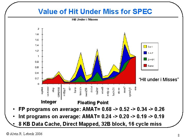
Value of Hit Under Miss for SPEC “Hit under i Misses” Integer Floating Point • FP programs on average: AMAT= 0. 68 > 0. 52 > 0. 34 > 0. 26 • Int programs on average: AMAT= 0. 24 > 0. 20 > 0. 19 • 8 KB Data Cache, Direct Mapped, 32 B block, 16 cycle miss © Alvin R. Lebeck 2006 8

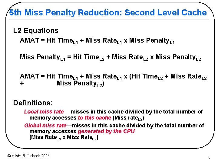
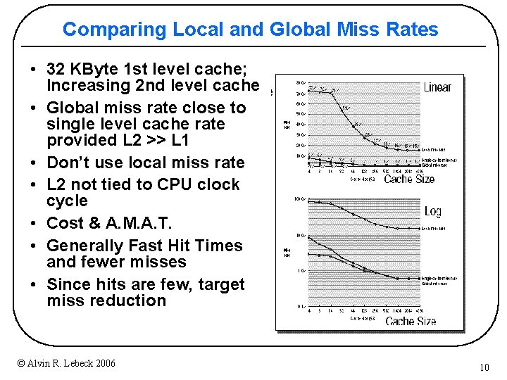
5 th Miss Penalty Reduction: Second Level Cache L 2 Equations AMAT = Hit Time. L 1 + Miss Rate. L 1 x Miss Penalty. L 1 = Hit Time. L 2 + Miss Rate. L 2 x Miss Penalty. L 2 AMAT = Hit Time. L 1 + Miss Rate. L 1 x (Hit Time. L 2 + Miss Rate. L 2 + Miss Penalty. L 2) Definitions: Local miss rate— misses in this cache divided by the total number of memory accesses to this cache (Miss rate. L 2) Global miss rate—misses in this cache divided by the total number of memory accesses generated by the CPU (Miss Rate. L 1 x Miss Rate. L 2) © Alvin R. Lebeck 2006 9

Comparing Local and Global Miss Rates • 32 KByte 1 st level cache; Increasing 2 nd level cache • Global miss rate close to single level cache rate provided L 2 >> L 1 • Don’t use local miss rate • L 2 not tied to CPU clock cycle • Cost & A. M. A. T. • Generally Fast Hit Times and fewer misses • Since hits are few, target miss reduction © Alvin R. Lebeck 2006 10

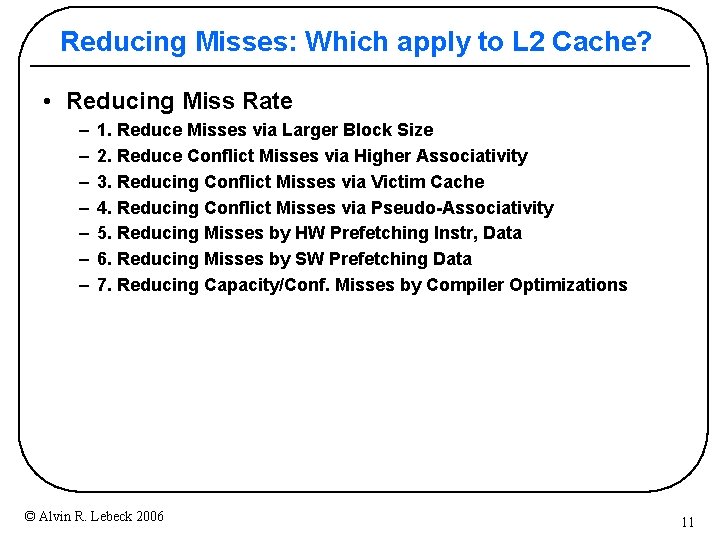
Reducing Misses: Which apply to L 2 Cache? • Reducing Miss Rate – – – – 1. Reduce Misses via Larger Block Size 2. Reduce Conflict Misses via Higher Associativity 3. Reducing Conflict Misses via Victim Cache 4. Reducing Conflict Misses via Pseudo Associativity 5. Reducing Misses by HW Prefetching Instr, Data 6. Reducing Misses by SW Prefetching Data 7. Reducing Capacity/Conf. Misses by Compiler Optimizations © Alvin R. Lebeck 2006 11

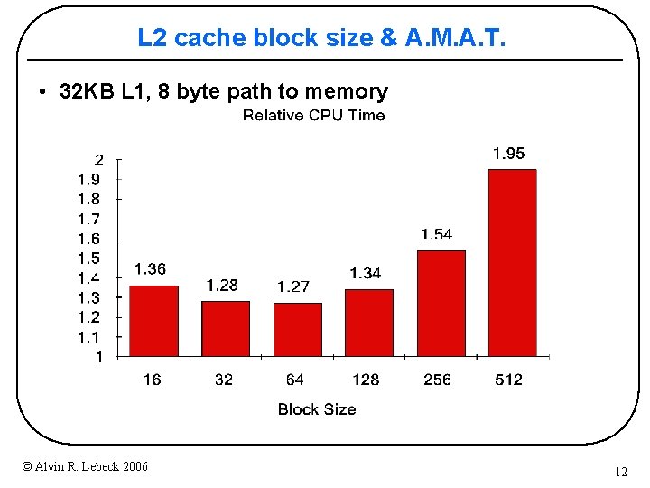
L 2 cache block size & A. M. A. T. • 32 KB L 1, 8 byte path to memory © Alvin R. Lebeck 2006 12

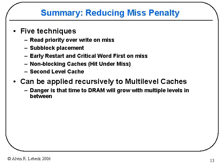
Summary: Reducing Miss Penalty • Five techniques – – – Read priority over write on miss Subblock placement Early Restart and Critical Word First on miss Non blocking Caches (Hit Under Miss) Second Level Cache • Can be applied recursively to Multilevel Caches – Danger is that time to DRAM will grow with multiple levels in between © Alvin R. Lebeck 2006 13

Review: Improving Cache Performance Ave Mem Acc Time = Hit time + (miss rate x miss penalty) 1. Reduce the miss rate, 2. Reduce the miss penalty, or 3. Reduce the time to hit in the cache. © Alvin R. Lebeck 2006 14

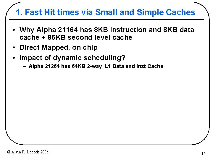
1. Fast Hit times via Small and Simple Caches • Why Alpha 21164 has 8 KB Instruction and 8 KB data cache + 96 KB second level cache • Direct Mapped, on chip • Impact of dynamic scheduling? – Alpha 21264 has 64 KB 2 way L 1 Data and Inst Cache © Alvin R. Lebeck 2006 15

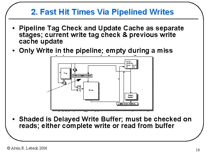
2. Fast Hit Times Via Pipelined Writes • Pipeline Tag Check and Update Cache as separate stages; current write tag check & previous write cache update • Only Write in the pipeline; empty during a miss • Shaded is Delayed Write Buffer; must be checked on reads; either complete write or read from buffer © Alvin R. Lebeck 2006 16

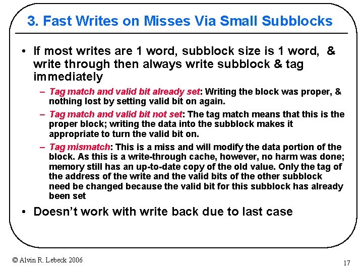
3. Fast Writes on Misses Via Small Subblocks • If most writes are 1 word, subblock size is 1 word, & write through then always write subblock & tag immediately – Tag match and valid bit already set: Writing the block was proper, & nothing lost by setting valid bit on again. – Tag match and valid bit not set: The tag match means that this is the proper block; writing the data into the subblock makes it appropriate to turn the valid bit on. – Tag mismatch: This is a miss and will modify the data portion of the block. As this is a write through cache, however, no harm was done; memory still has an up to date copy of the old value. Only the tag of the address of the write and the valid bits of the other subblock need be changed because the valid bit for this subblock has already been set • Doesn’t work with write back due to last case © Alvin R. Lebeck 2006 17

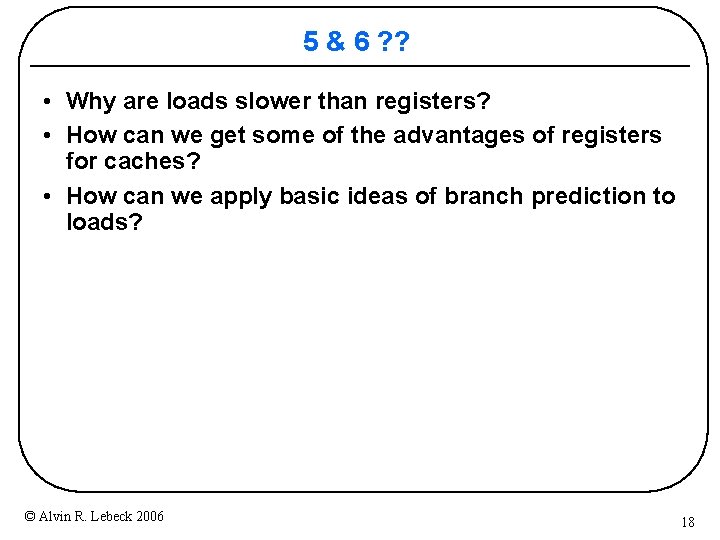
5 & 6 ? ? • Why are loads slower than registers? • How can we get some of the advantages of registers for caches? • How can we apply basic ideas of branch prediction to loads? © Alvin R. Lebeck 2006 18

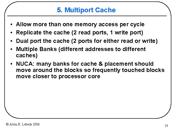
5. Multiport Cache • • Allow more than one memory access per cycle Replicate the cache (2 read ports, 1 write port) Dual port the cache (2 ports for either read or write) Multiple Banks (different addresses to different caches) • NUCA: many banks for cache & placement should move around the blocks so frequently touched blocks move closer to processor core © Alvin R. Lebeck 2006 19

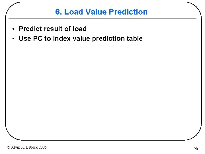
6. Load Value Prediction • Predict result of load • Use PC to index value prediction table © Alvin R. Lebeck 2006 20

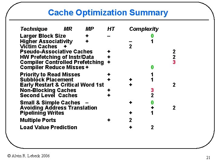
Cache Optimization Summary Technique MR MP Larger Block Size + Higher Associativity + Victim Caches + Pseudo Associative Caches HW Prefetching of Instr/Data Compiler Controlled Prefetching Compiler Reduce Misses + Priority to Read Misses Subblock Placement Early Restart & Critical Word 1 st Non Blocking Caches Second Level Caches Small & Simple Caches – Avoiding Address Translation Pipelining Writes Multiple Ports Load Value Prediction © Alvin R. Lebeck 2006 HT – + + + + Complexity 0 – 1 2 + + + 2 + 0 1 1 3 2 0 + 1 2 2 3 2 21

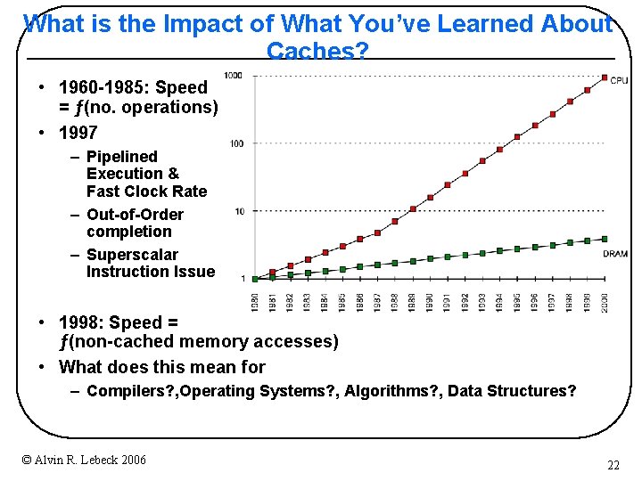
What is the Impact of What You’ve Learned About Caches? • 1960 1985: Speed = ƒ(no. operations) • 1997 – Pipelined Execution & Fast Clock Rate – Out of Order completion – Superscalar Instruction Issue • 1998: Speed = ƒ(non cached memory accesses) • What does this mean for – Compilers? , Operating Systems? , Algorithms? , Data Structures? © Alvin R. Lebeck 2006 22

Memory Hierarchy— Main Memory and Enhancing its Performance

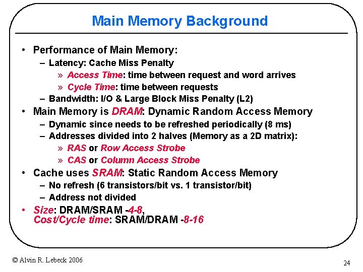
Main Memory Background • Performance of Main Memory: – Latency: Cache Miss Penalty » Access Time: time between request and word arrives » Cycle Time: time between requests – Bandwidth: I/O & Large Block Miss Penalty (L 2) • Main Memory is DRAM: Dynamic Random Access Memory – Dynamic since needs to be refreshed periodically (8 ms) – Addresses divided into 2 halves (Memory as a 2 D matrix): » RAS or Row Access Strobe » CAS or Column Access Strobe • Cache uses SRAM: Static Random Access Memory – No refresh (6 transistors/bit vs. 1 transistor/bit) – Address not divided • Size: DRAM/SRAM 4 -8, Cost/Cycle time: SRAM/DRAM 8 -16 © Alvin R. Lebeck 2006 24

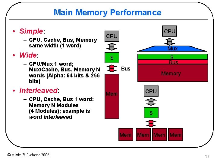
Main Memory Performance • Simple: – CPU, Cache, Bus, Memory same width (1 word) • Wide: – CPU/Mux 1 word; Mux/Cache, Bus, Memory N words (Alpha: 64 bits & 256 bits) • Interleaved: – CPU, Cache, Bus 1 word: Memory N Modules (4 Modules); example is word interleaved CPU Mux $ Bus CPU Mem $ Mem © Alvin R. Lebeck 2006 Memory Mem Mem 25

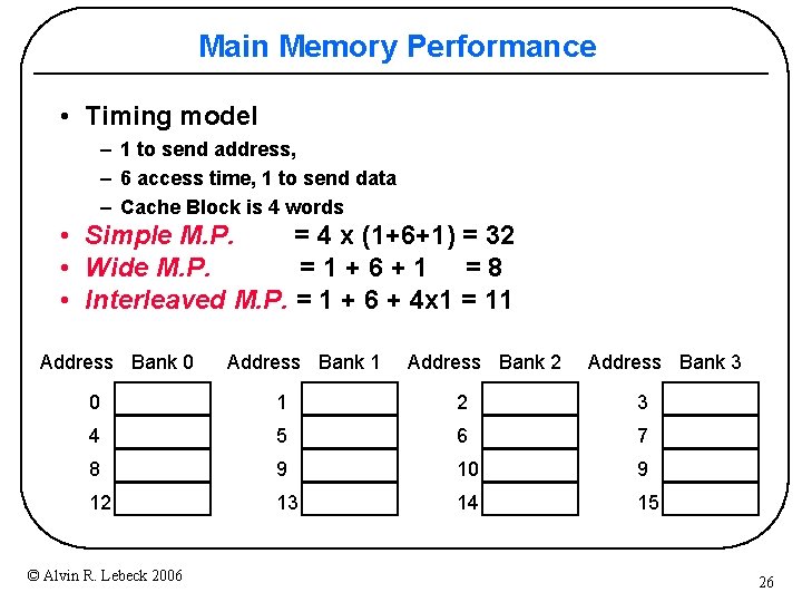
Main Memory Performance • Timing model – 1 to send address, – 6 access time, 1 to send data – Cache Block is 4 words • Simple M. P. = 4 x (1+6+1) = 32 • Wide M. P. =1+6+1 =8 • Interleaved M. P. = 1 + 6 + 4 x 1 = 11 Address Bank 0 Address Bank 1 Address Bank 2 Address Bank 3 0 1 2 3 4 5 6 7 8 9 10 9 12 13 14 15 © Alvin R. Lebeck 2006 26

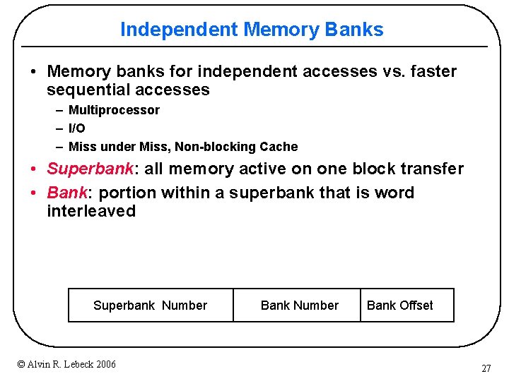
Independent Memory Banks • Memory banks for independent accesses vs. faster sequential accesses – Multiprocessor – I/O – Miss under Miss, Non blocking Cache • Superbank: all memory active on one block transfer • Bank: portion within a superbank that is word interleaved Superbank Number © Alvin R. Lebeck 2006 Bank Number Bank Offset 27

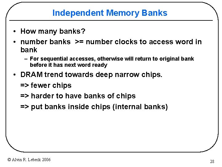
Independent Memory Banks • How many banks? • number banks >= number clocks to access word in bank – For sequential accesses, otherwise will return to original bank before it has next word ready • DRAM trend towards deep narrow chips. => fewer chips => harder to have banks of chips => put banks inside chips (internal banks) © Alvin R. Lebeck 2006 28
![Avoiding Bank Conflicts Lots of banks int x256512 for j 0 j Avoiding Bank Conflicts • Lots of banks int x[256][512]; for (j = 0; j](https://slidetodoc.com/presentation_image/1321bbc33e5db30f8e26e5eda97ca35d/image-29.jpg)
Avoiding Bank Conflicts • Lots of banks int x[256][512]; for (j = 0; j < 512; j = j+1) for (i = 0; i < 256; i = i+1) x[i][j] = 2 * x[i][j]; • Even with 128 banks, since 512 is multiple of 128, conflict – structural hazard • SW: loop interchange or declaring array not power of 2 • HW: Prime number of banks – – – bank number = address mod number of banks address within bank = address / number of banks modulo & divide per memory access? address within bank = address mod number words in bank (3, 7, 31) bank number? easy if 2 N words per bank © Alvin R. Lebeck 2006 29

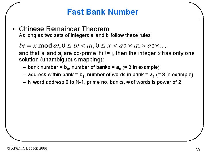
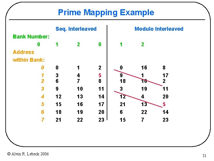
Fast Bank Number • Chinese Remainder Theorem As long as two sets of integers ai and bi follow these rules and that ai and aj are co-prime if i != j, then the integer x has only one solution (unambiguous mapping): – bank number = b 0, number of banks = a 0 (= 3 in example) – address within bank = b 1, number of words in bank = a 1 (= 8 in example) – N word address 0 to N-1, prime no. banks, # of words is power of 2 © Alvin R. Lebeck 2006 30

Prime Mapping Example Seq. Interleaved Bank Number: 0 Address within Bank: 0 1 2 3 4 5 6 7 © Alvin R. Lebeck 2006 Modulo Interleaved 1 2 0 3 6 9 12 15 18 21 1 4 7 10 13 16 19 22 2 5 8 11 14 17 20 23 0 9 18 3 12 21 6 15 16 1 10 19 4 13 22 7 8 17 2 11 20 5 14 23 31

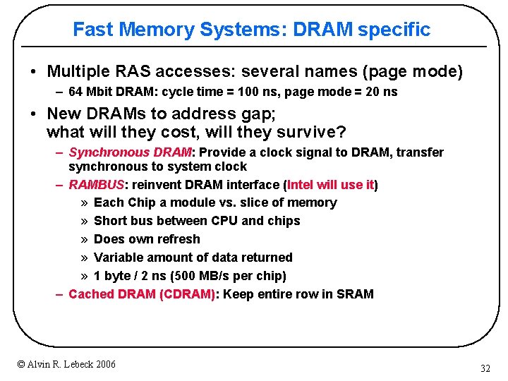
Fast Memory Systems: DRAM specific • Multiple RAS accesses: several names (page mode) – 64 Mbit DRAM: cycle time = 100 ns, page mode = 20 ns • New DRAMs to address gap; what will they cost, will they survive? – Synchronous DRAM: Provide a clock signal to DRAM, transfer synchronous to system clock – RAMBUS: reinvent DRAM interface (Intel will use it) » Each Chip a module vs. slice of memory » Short bus between CPU and chips » Does own refresh » Variable amount of data returned » 1 byte / 2 ns (500 MB/s per chip) – Cached DRAM (CDRAM): Keep entire row in SRAM © Alvin R. Lebeck 2006 32

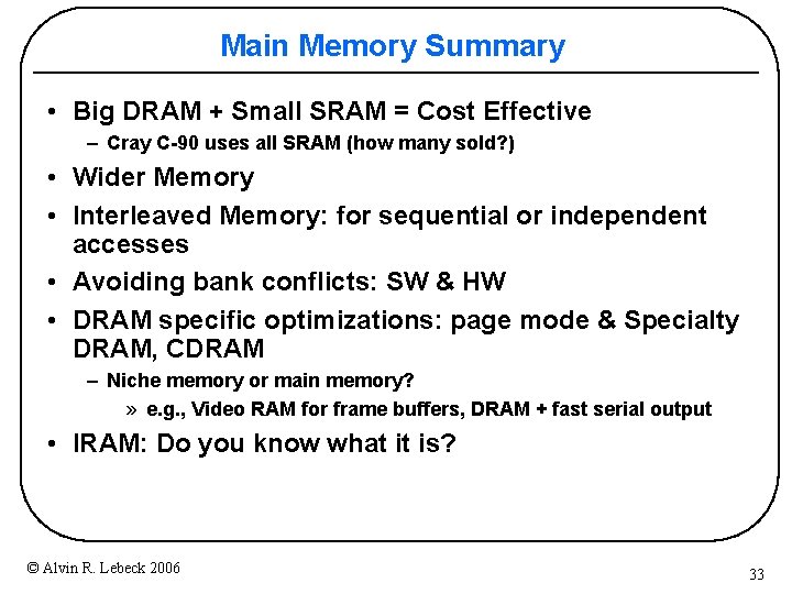
Main Memory Summary • Big DRAM + Small SRAM = Cost Effective – Cray C 90 uses all SRAM (how many sold? ) • Wider Memory • Interleaved Memory: for sequential or independent accesses • Avoiding bank conflicts: SW & HW • DRAM specific optimizations: page mode & Specialty DRAM, CDRAM – Niche memory or main memory? » e. g. , Video RAM for frame buffers, DRAM + fast serial output • IRAM: Do you know what it is? © Alvin R. Lebeck 2006 33

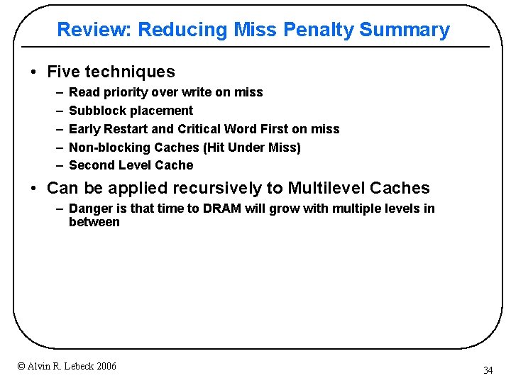
Review: Reducing Miss Penalty Summary • Five techniques – – – Read priority over write on miss Subblock placement Early Restart and Critical Word First on miss Non blocking Caches (Hit Under Miss) Second Level Cache • Can be applied recursively to Multilevel Caches – Danger is that time to DRAM will grow with multiple levels in between © Alvin R. Lebeck 2006 34

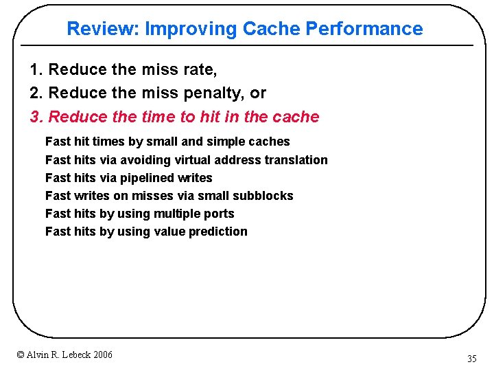
Review: Improving Cache Performance 1. Reduce the miss rate, 2. Reduce the miss penalty, or 3. Reduce the time to hit in the cache Fast hit times by small and simple caches Fast hits via avoiding virtual address translation Fast hits via pipelined writes Fast writes on misses via small subblocks Fast hits by using multiple ports Fast hits by using value prediction © Alvin R. Lebeck 2006 35

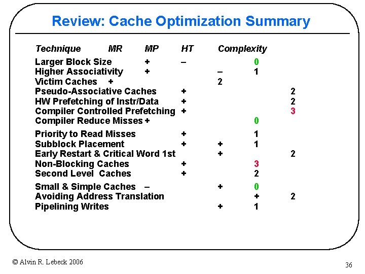
Review: Cache Optimization Summary Technique MR MP Larger Block Size + Higher Associativity + Victim Caches + Pseudo Associative Caches HW Prefetching of Instr/Data Compiler Controlled Prefetching Compiler Reduce Misses + Priority to Read Misses Subblock Placement Early Restart & Critical Word 1 st Non Blocking Caches Second Level Caches Small & Simple Caches – Avoiding Address Translation Pipelining Writes © Alvin R. Lebeck 2006 HT – + + + + Complexity 0 – 1 2 + + 0 1 1 3 2 0 + 1 2 2 36

Next Time • Memory hierarchy and virtual memory © Alvin R. Lebeck 2006 37