Memory Hierarchy 1 Outline RandomAccess Memory RAM Nonvolatile


![Locality • Data locality int sumvec(int v[N]) { int i, sum = 0 ; Locality • Data locality int sumvec(int v[N]) { int i, sum = 0 ;](https://slidetodoc.com/presentation_image_h2/4e2ffdefa612c0c5730cb4394ba9e030/image-50.jpg)
![Locality • Example (pp. 480, M=2, N=3) int sumvec(int v[M][N]) { int i, j, Locality • Example (pp. 480, M=2, N=3) int sumvec(int v[M][N]) { int i, j,](https://slidetodoc.com/presentation_image_h2/4e2ffdefa612c0c5730cb4394ba9e030/image-56.jpg)
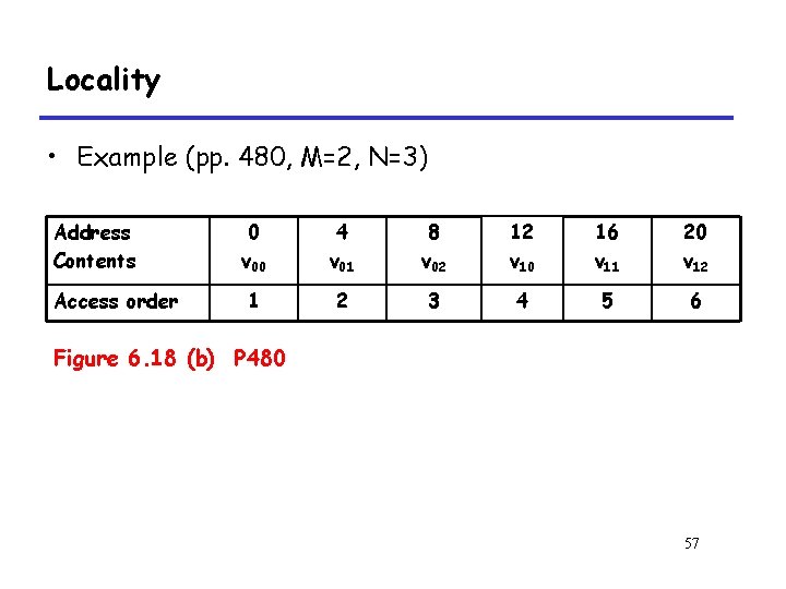
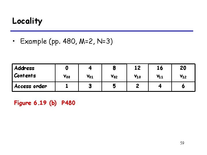
![Locality • Example (pp. 480, M=2, N=3) int sumvec(int v[M][N]) { int i, j, Locality • Example (pp. 480, M=2, N=3) int sumvec(int v[M][N]) { int i, j,](https://slidetodoc.com/presentation_image_h2/4e2ffdefa612c0c5730cb4394ba9e030/image-58.jpg)
- Slides: 79

Memory Hierarchy 1

Outline • Random-Access Memory (RAM) • Nonvolatile Memory • Disk Storage • Locality • Memory hierarchy • Suggested Reading: 6. 1, 6. 2, 6. 3 Nonvolatile: 非易失的 2

6. 1 Storage Technologies 3

6. 1. 1 Random-Access Memory 4

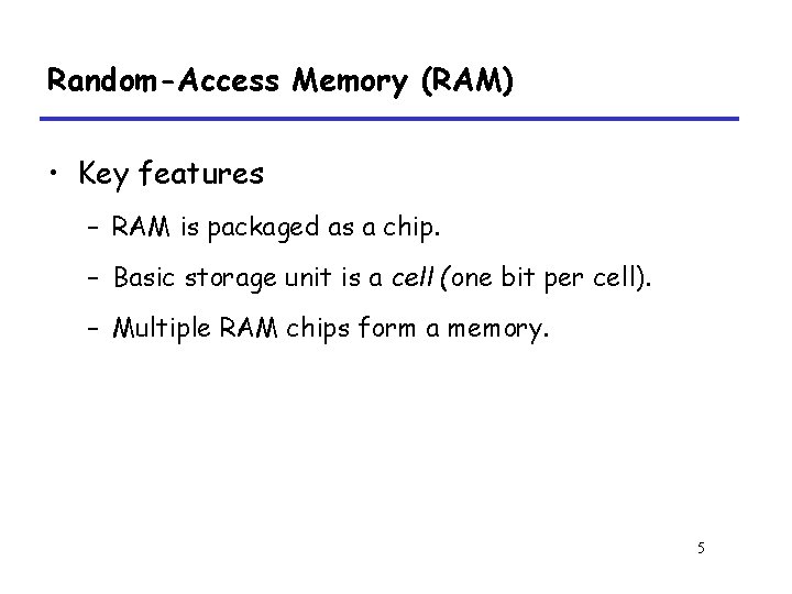
Random-Access Memory (RAM) • Key features – RAM is packaged as a chip. – Basic storage unit is a cell (one bit per cell). – Multiple RAM chips form a memory. 5

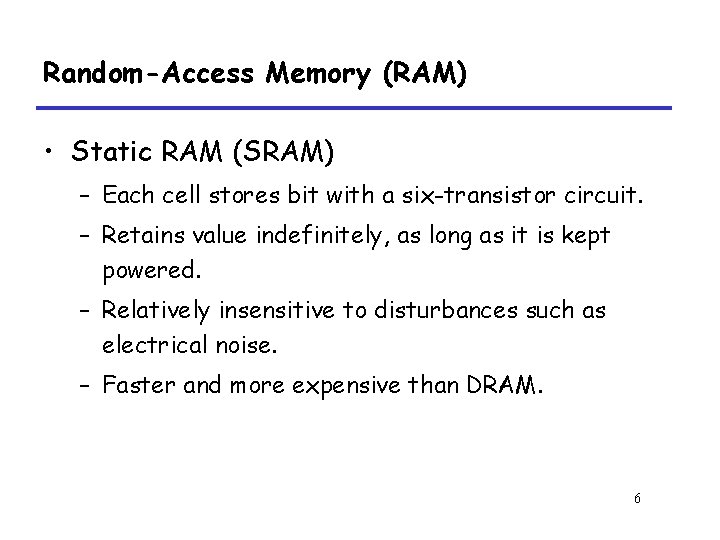
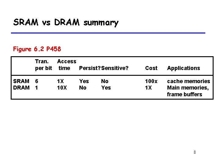
Random-Access Memory (RAM) • Static RAM (SRAM) – Each cell stores bit with a six-transistor circuit. – Retains value indefinitely, as long as it is kept powered. – Relatively insensitive to disturbances such as electrical noise. – Faster and more expensive than DRAM. 6

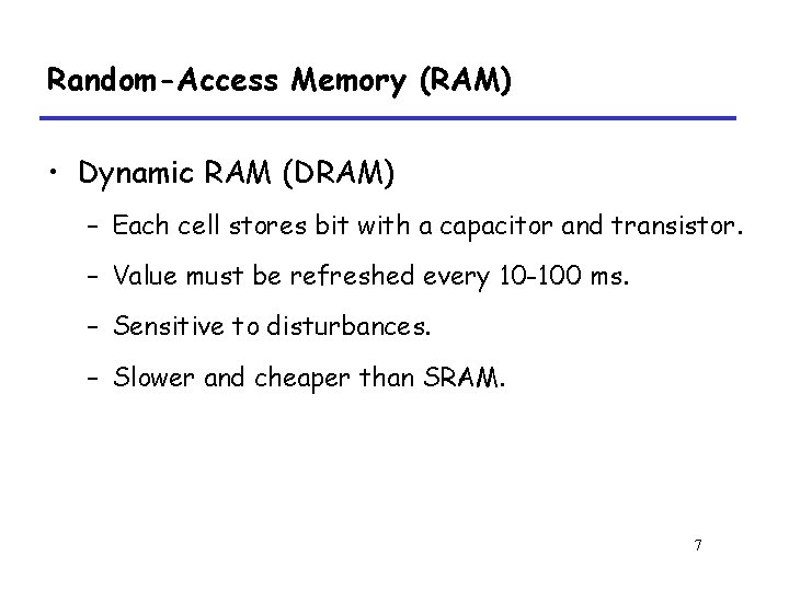
Random-Access Memory (RAM) • Dynamic RAM (DRAM) – Each cell stores bit with a capacitor and transistor. – Value must be refreshed every 10 -100 ms. – Sensitive to disturbances. – Slower and cheaper than SRAM. 7

SRAM vs DRAM summary Figure 6. 2 P 458 SRAM DRAM Tran. Access per bit time Persist? Sensitive? Cost Applications 6 1 100 x 1 X cache memories Main memories, frame buffers 1 X 10 X Yes No No Yes 8

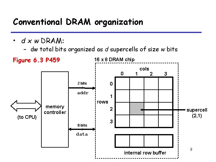
Conventional DRAM organization • d x w DRAM: – dw total bits organized as d supercells of size w bits Figure 6. 3 P 459 16 x 8 DRAM chip 0 2 bits / 2 3 0 addr (to CPU) 1 cols 1 rows memory controller 2 8 bits / supercell (2, 1) 3 data internal row buffer 9

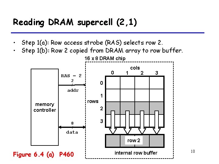
Reading DRAM supercell (2, 1) • Step 1(a): Row access strobe (RAS) selects row 2. • Step 1(b): Row 2 copied from DRAM array to row buffer. 16 x 8 DRAM chip 0 RAS = 2 2 / 1 cols 2 3 0 addr 1 rows memory controller 2 8 / 3 data row 2 Figure 6. 4 (a) P 460 internal row buffer 10

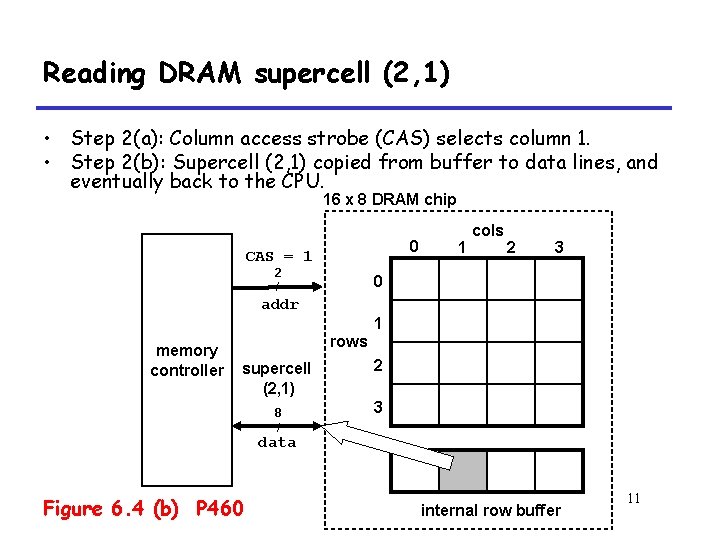
Reading DRAM supercell (2, 1) • Step 2(a): Column access strobe (CAS) selects column 1. • Step 2(b): Supercell (2, 1) copied from buffer to data lines, and eventually back to the CPU. 16 x 8 DRAM chip 0 CAS = 1 2 / 1 cols 2 3 0 addr 1 memory controller rows supercell (2, 1) 8 / 2 3 data Figure 6. 4 (b) P 460 internal row buffer 11

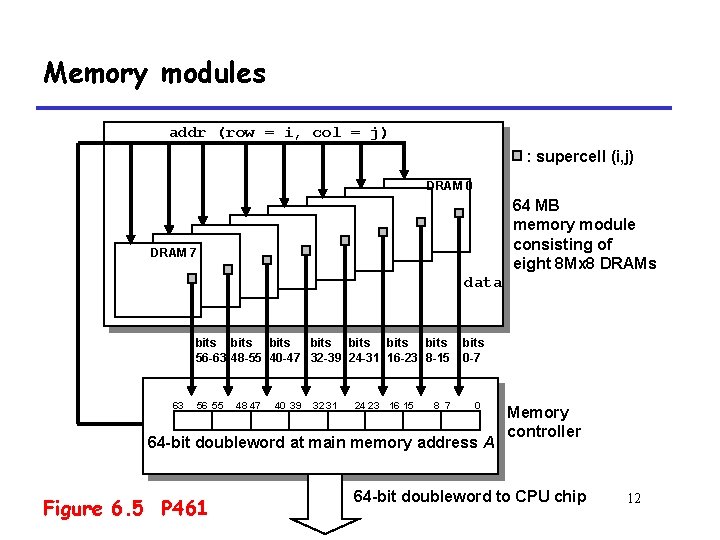
Memory modules addr (row = i, col = j) : supercell (i, j) DRAM 0 64 MB memory module consisting of eight 8 Mx 8 DRAMs DRAM 7 data bits bits 56 -63 48 -55 40 -47 32 -39 24 -31 16 -23 8 -15 63 56 55 48 47 40 39 32 31 24 23 16 15 8 7 bits 0 -7 0 64 -bit doubleword at main memory address A Figure 6. 5 P 461 Memory controller 64 -bit doubleword to CPU chip 12

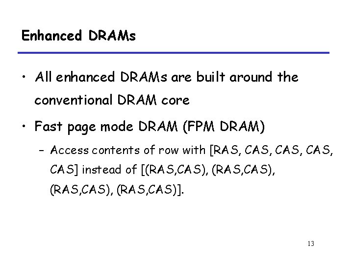
Enhanced DRAMs • All enhanced DRAMs are built around the conventional DRAM core • Fast page mode DRAM (FPM DRAM) – Access contents of row with [RAS, CAS, CAS] instead of [(RAS, CAS), (RAS, CAS)]. 13

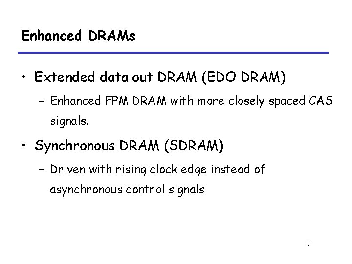
Enhanced DRAMs • Extended data out DRAM (EDO DRAM) – Enhanced FPM DRAM with more closely spaced CAS signals. • Synchronous DRAM (SDRAM) – Driven with rising clock edge instead of asynchronous control signals 14

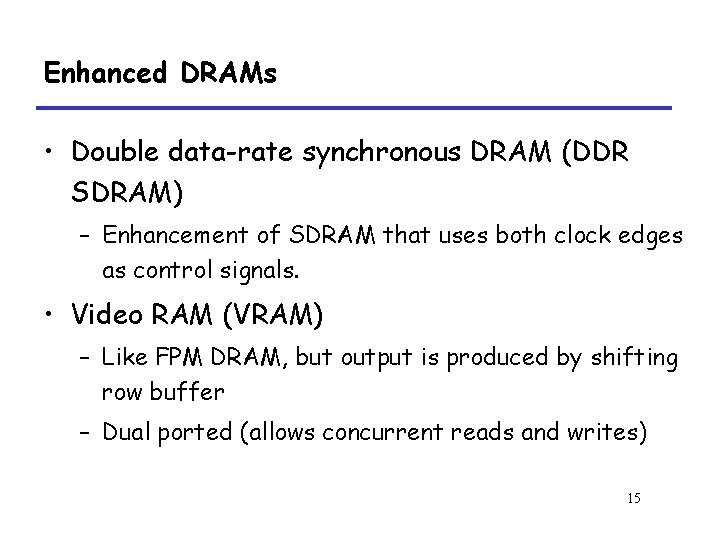
Enhanced DRAMs • Double data-rate synchronous DRAM (DDR SDRAM) – Enhancement of SDRAM that uses both clock edges as control signals. • Video RAM (VRAM) – Like FPM DRAM, but output is produced by shifting row buffer – Dual ported (allows concurrent reads and writes) 15

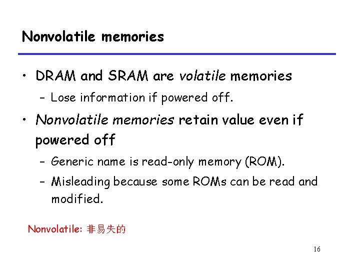
Nonvolatile memories • DRAM and SRAM are volatile memories – Lose information if powered off. • Nonvolatile memories retain value even if powered off – Generic name is read-only memory (ROM). – Misleading because some ROMs can be read and modified. Nonvolatile: 非易失的 16

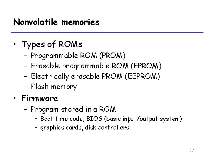
Nonvolatile memories • Types of ROMs – – Programmable ROM (PROM) Erasable programmable ROM (EPROM) Electrically erasable PROM (EEPROM) Flash memory • Firmware – Program stored in a ROM • Boot time code, BIOS (basic input/output system) • graphics cards, disk controllers 17

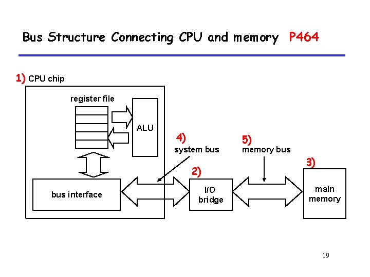
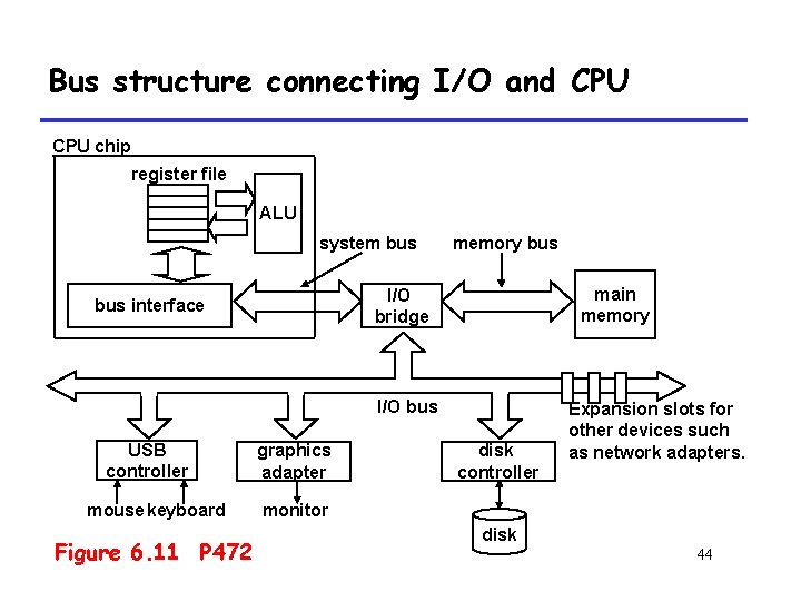
Bus Structure Connecting CPU and memory • A bus is a collection of parallel wires that carry address, data, and control signals • Buses are typically shared by multiple devices 18

Bus Structure Connecting CPU and memory P 464 1) CPU chip register file ALU 4) system bus 2) bus interface I/O bridge 5) memory bus 3) main memory 19

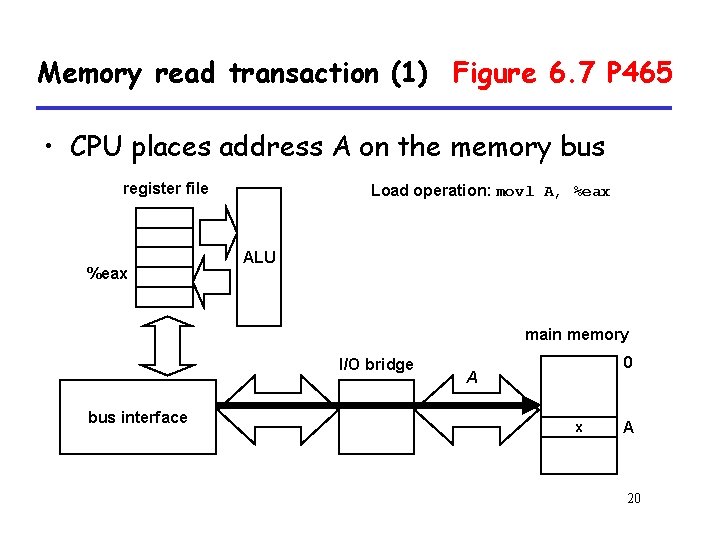
Memory read transaction (1) Figure 6. 7 P 465 • CPU places address A on the memory bus register file %eax Load operation: movl A, %eax ALU main memory I/O bridge bus interface 0 A x A 20

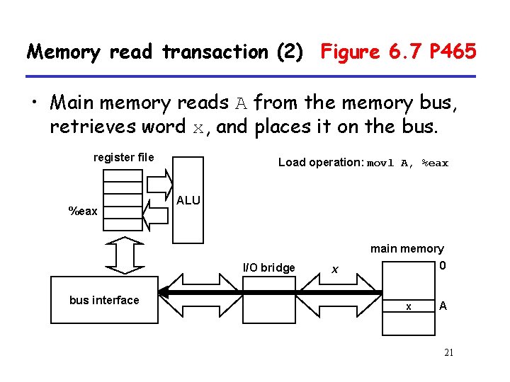
Memory read transaction (2) Figure 6. 7 P 465 • Main memory reads A from the memory bus, retrieves word x, and places it on the bus. register file %eax Load operation: movl A, %eax ALU main memory I/O bridge bus interface 0 x x A 21

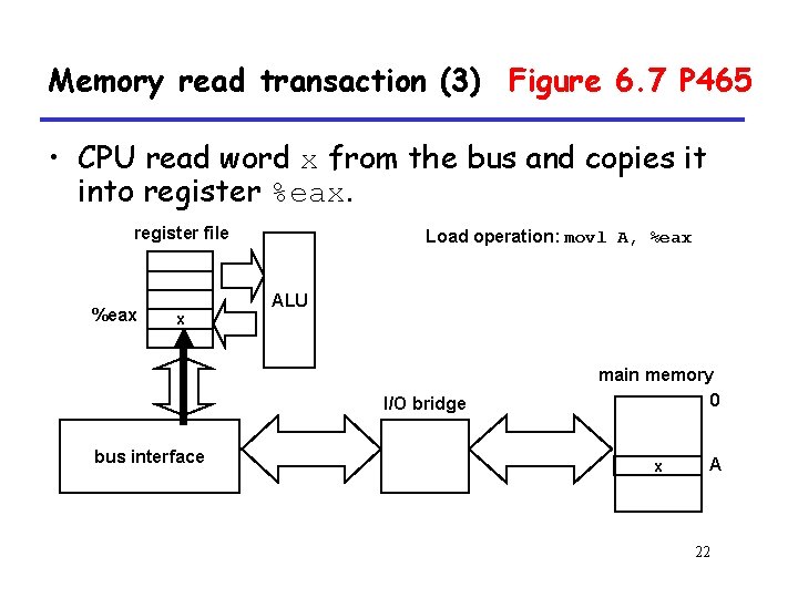
Memory read transaction (3) Figure 6. 7 P 465 • CPU read word x from the bus and copies it into register %eax. register file %eax Load operation: movl A, %eax ALU x I/O bridge bus interface main memory 0 x A 22

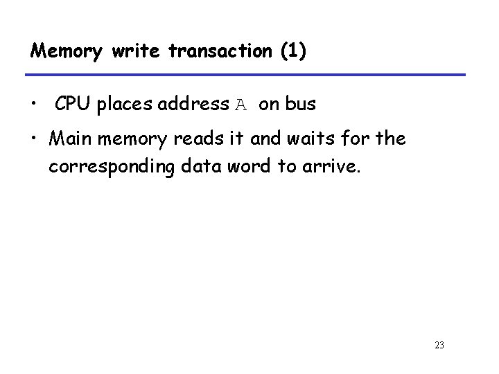
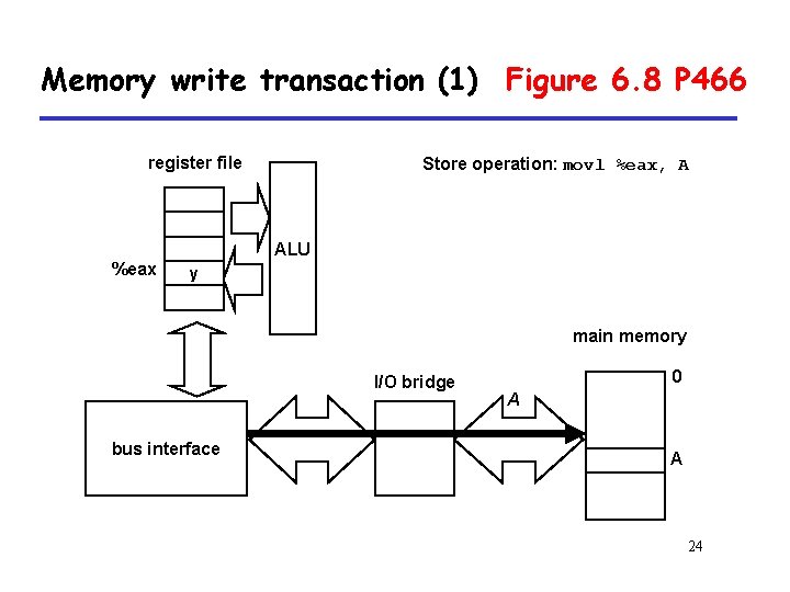
Memory write transaction (1) • CPU places address A on bus • Main memory reads it and waits for the corresponding data word to arrive. 23

Memory write transaction (1) Figure 6. 8 P 466 register file Store operation: movl %eax, A ALU %eax y main memory I/O bridge bus interface 0 A A 24

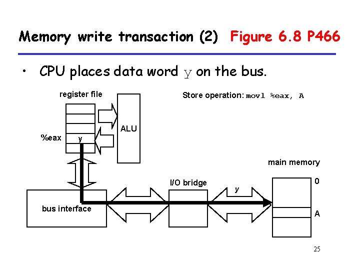
Memory write transaction (2) Figure 6. 8 P 466 • CPU places data word y on the bus. register file %eax Store operation: movl %eax, A ALU y main memory I/O bridge bus interface y 0 A 25

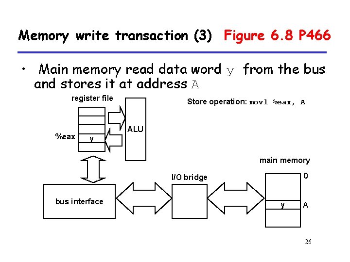
Memory write transaction (3) Figure 6. 8 P 466 • Main memory read data word y from the bus and stores it at address A register file %eax Store operation: movl %eax, A ALU y main memory 0 I/O bridge bus interface y A 26

6. 1. 2 Disk Storage 27

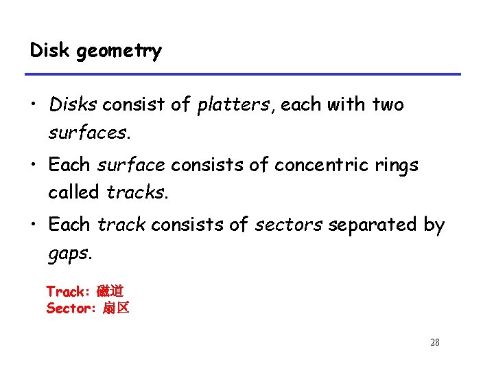
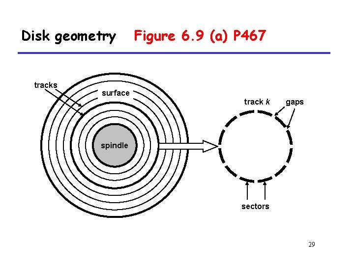
Disk geometry • Disks consist of platters, each with two surfaces. • Each surface consists of concentric rings called tracks. • Each track consists of sectors separated by gaps. Track: 磁道 Sector: 扇区 28

Disk geometry tracks Figure 6. 9 (a) P 467 surface track k gaps spindle sectors 29

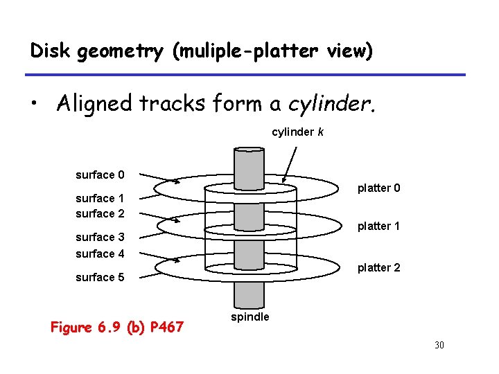
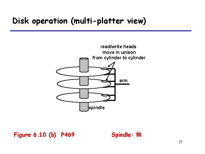
Disk geometry (muliple-platter view) • Aligned tracks form a cylinder k surface 0 platter 0 surface 1 surface 2 platter 1 surface 3 surface 4 platter 2 surface 5 Figure 6. 9 (b) P 467 spindle 30

Disk capacity • Capacity – maximum number of bits that can be stored – Vendors express capacity in units of gigabytes (GB), where 1 GB = 10^9. 31

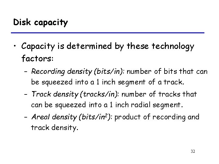
Disk capacity • Capacity is determined by these technology factors: – Recording density (bits/in): number of bits that can be squeezed into a 1 inch segment of a track. – Track density (tracks/in): number of tracks that can be squeezed into a 1 inch radial segment. – Areal density (bits/in 2): product of recording and track density. 32

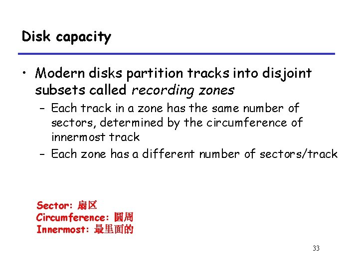
Disk capacity • Modern disks partition tracks into disjoint subsets called recording zones – Each track in a zone has the same number of sectors, determined by the circumference of innermost track – Each zone has a different number of sectors/track Sector: 扇区 Circumference: 圆周 Innermost: 最里面的 33

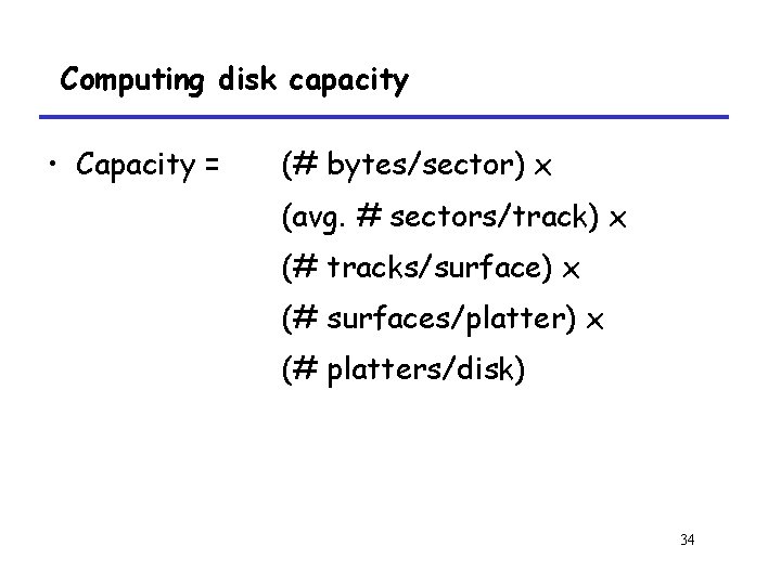
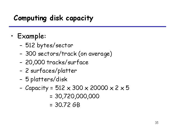
Computing disk capacity • Capacity = (# bytes/sector) x (avg. # sectors/track) x (# tracks/surface) x (# surfaces/platter) x (# platters/disk) 34

Computing disk capacity • Example: – – – 512 bytes/sector 300 sectors/track (on average) 20, 000 tracks/surface 2 surfaces/platter 5 platters/disk Capacity = 512 x 300 x 20000 x 2 x 5 = 30, 720, 000 = 30. 72 GB 35

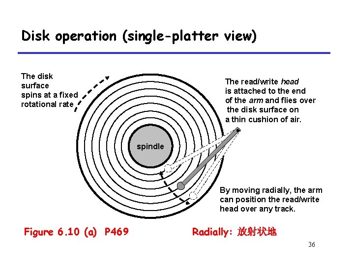
Disk operation (single-platter view) The disk surface spins at a fixed rotational rate The read/write head is attached to the end of the arm and flies over the disk surface on a thin cushion of air. spindle By moving radially, the arm can position the read/write head over any track. Figure 6. 10 (a) P 469 Radially: 放射状地 36

Disk operation (multi-platter view) read/write heads move in unison from cylinder to cylinder arm spindle Figure 6. 10 (b) P 469 Spindle: 轴 37

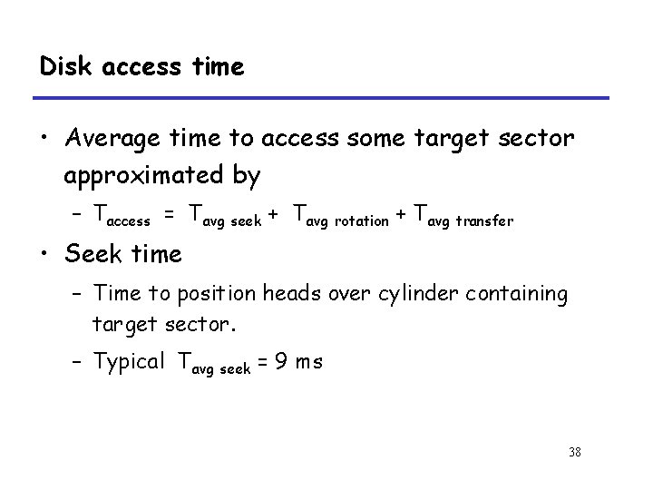
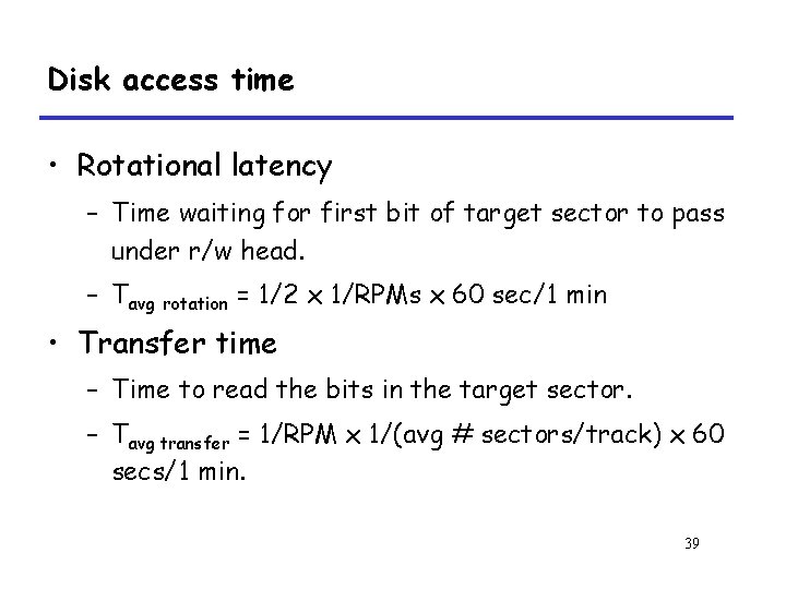
Disk access time • Average time to access some target sector approximated by – Taccess = Tavg seek + Tavg rotation + Tavg transfer • Seek time – Time to position heads over cylinder containing target sector. – Typical Tavg seek = 9 ms 38

Disk access time • Rotational latency – Time waiting for first bit of target sector to pass under r/w head. – Tavg rotation = 1/2 x 1/RPMs x 60 sec/1 min • Transfer time – Time to read the bits in the target sector. – Tavg transfer = 1/RPM x 1/(avg # sectors/track) x 60 secs/1 min. 39

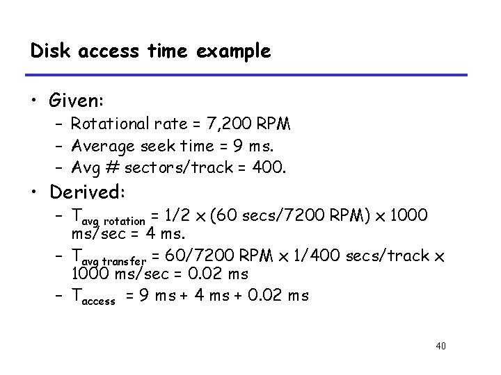
Disk access time example • Given: – Rotational rate = 7, 200 RPM – Average seek time = 9 ms. – Avg # sectors/track = 400. • Derived: – Tavg rotation = 1/2 x (60 secs/7200 RPM) x 1000 ms/sec = 4 ms. – Tavg transfer = 60/7200 RPM x 1/400 secs/track x 1000 ms/sec = 0. 02 ms – Taccess = 9 ms + 4 ms + 0. 02 ms 40

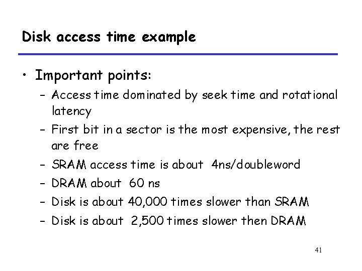
Disk access time example • Important points: – Access time dominated by seek time and rotational latency – First bit in a sector is the most expensive, the rest are free – SRAM access time is about 4 ns/doubleword – DRAM about 60 ns – Disk is about 40, 000 times slower than SRAM – Disk is about 2, 500 times slower then DRAM 41

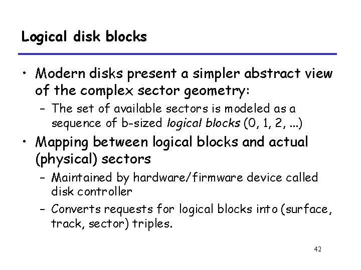
Logical disk blocks • Modern disks present a simpler abstract view of the complex sector geometry: – The set of available sectors is modeled as a sequence of b-sized logical blocks (0, 1, 2, . . . ) • Mapping between logical blocks and actual (physical) sectors – Maintained by hardware/firmware device called disk controller – Converts requests for logical blocks into (surface, track, sector) triples. 42

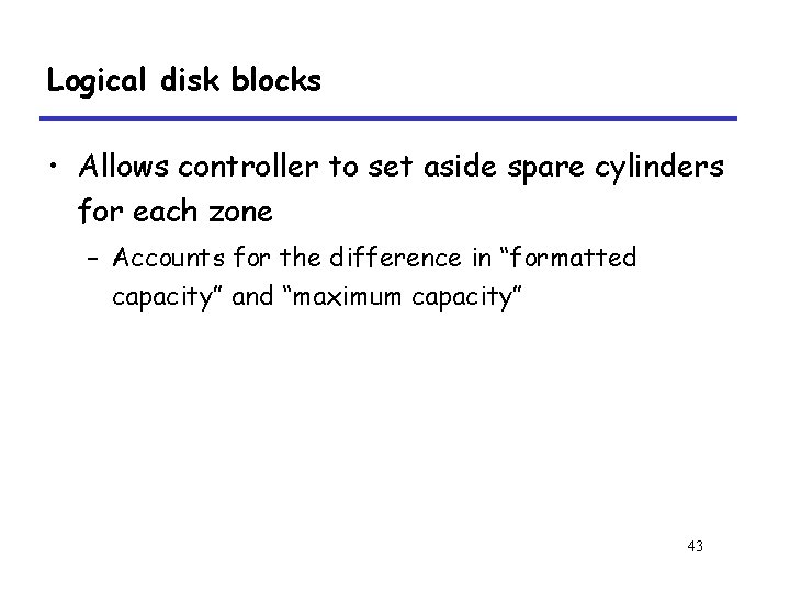
Logical disk blocks • Allows controller to set aside spare cylinders for each zone – Accounts for the difference in “formatted capacity” and “maximum capacity” 43

Bus structure connecting I/O and CPU chip register file ALU system bus memory bus main memory I/O bridge bus interface I/O bus USB controller mouse keyboard Figure 6. 11 P 472 graphics adapter disk controller Expansion slots for other devices such as network adapters. monitor disk 44

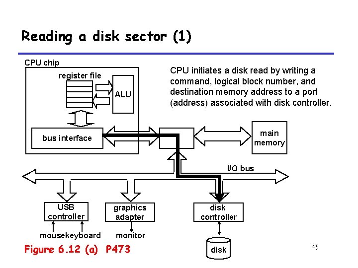
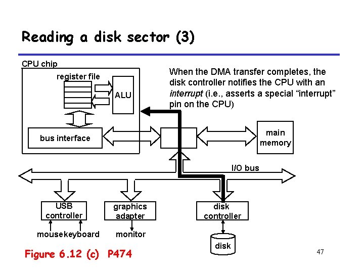
Reading a disk sector (1) CPU chip register file ALU CPU initiates a disk read by writing a command, logical block number, and destination memory address to a port (address) associated with disk controller. main memory bus interface I/O bus USB controller mousekeyboard graphics adapter disk controller monitor Figure 6. 12 (a) P 473 disk 45

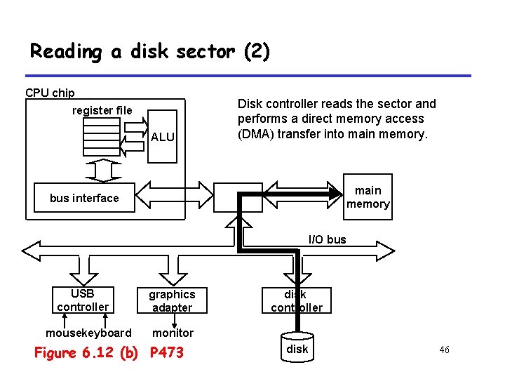
Reading a disk sector (2) CPU chip register file ALU Disk controller reads the sector and performs a direct memory access (DMA) transfer into main memory bus interface I/O bus USB controller mousekeyboard graphics adapter disk controller monitor Figure 6. 12 (b) P 473 disk 46

Reading a disk sector (3) CPU chip register file ALU When the DMA transfer completes, the disk controller notifies the CPU with an interrupt (i. e. , asserts a special “interrupt” pin on the CPU) main memory bus interface I/O bus USB controller mousekeyboard graphics adapter disk controller monitor Figure 6. 12 (c) P 474 disk 47

6. 1. 3 Storage Technology Trends 48

6. 2 Locality 49
![Locality Data locality int sumvecint vN int i sum 0 Locality • Data locality int sumvec(int v[N]) { int i, sum = 0 ;](https://slidetodoc.com/presentation_image_h2/4e2ffdefa612c0c5730cb4394ba9e030/image-50.jpg)
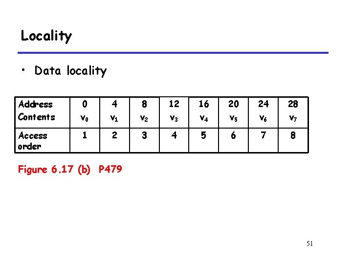
Locality • Data locality int sumvec(int v[N]) { int i, sum = 0 ; for (i = 0 ; i < N ; i++) sum += v[i] ; return sum ; } Figure 6. 17 (a) P 479 50

Locality • Data locality Address Contents 0 v 0 4 v 1 8 v 2 12 v 3 16 v 4 20 v 5 24 v 6 28 v 7 Access order 1 2 3 4 5 6 7 8 Figure 6. 17 (b) P 479 51

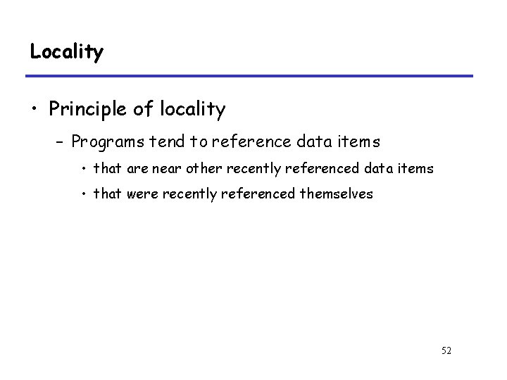
Locality • Principle of locality – Programs tend to reference data items • that are near other recently referenced data items • that were recently referenced themselves 52

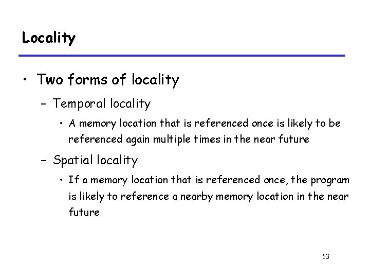
Locality • Two forms of locality – Temporal locality • A memory location that is referenced once is likely to be referenced again multiple times in the near future – Spatial locality • If a memory location that is referenced once, the program is likely to reference a nearby memory location in the near future 53

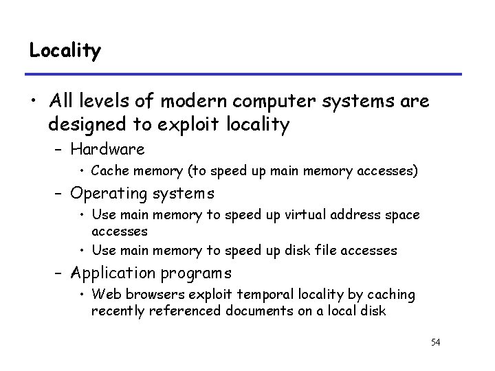
Locality • All levels of modern computer systems are designed to exploit locality – Hardware • Cache memory (to speed up main memory accesses) – Operating systems • Use main memory to speed up virtual address space accesses • Use main memory to speed up disk file accesses – Application programs • Web browsers exploit temporal locality by caching recently referenced documents on a local disk 54

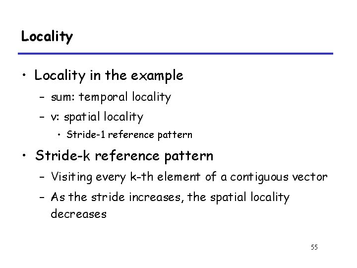
Locality • Locality in the example – sum: temporal locality – v: spatial locality • Stride-1 reference pattern • Stride-k reference pattern – Visiting every k-th element of a contiguous vector – As the stride increases, the spatial locality decreases 55
![Locality Example pp 480 M2 N3 int sumvecint vMN int i j Locality • Example (pp. 480, M=2, N=3) int sumvec(int v[M][N]) { int i, j,](https://slidetodoc.com/presentation_image_h2/4e2ffdefa612c0c5730cb4394ba9e030/image-56.jpg)
Locality • Example (pp. 480, M=2, N=3) int sumvec(int v[M][N]) { int i, j, sum = 0 ; for (i = 0 ; i < M ; i++) for ( j = 0 ; j < N ; j++ ) sum += v[i][j] ; return sum ; } Figure 6. 18 (a) P 480 56

Locality • Example (pp. 480, M=2, N=3) Address Contents Access order 0 v 00 4 v 01 8 v 02 12 v 10 16 v 11 20 v 12 1 2 3 4 5 6 Figure 6. 18 (b) P 480 57
![Locality Example pp 480 M2 N3 int sumvecint vMN int i j Locality • Example (pp. 480, M=2, N=3) int sumvec(int v[M][N]) { int i, j,](https://slidetodoc.com/presentation_image_h2/4e2ffdefa612c0c5730cb4394ba9e030/image-58.jpg)
Locality • Example (pp. 480, M=2, N=3) int sumvec(int v[M][N]) { int i, j, sum = 0 ; for (j = 0 ; j < N ; j++) for ( i = 0 ; i < M ; i++ ) sum += v[i][j] ; return sum ; } Figure 6. 19 (a) P 480 58

Locality • Example (pp. 480, M=2, N=3) Address Contents Access order 0 v 00 4 v 01 8 v 02 12 v 10 16 v 11 20 v 12 1 3 5 2 4 6 Figure 6. 19 (b) P 480 59

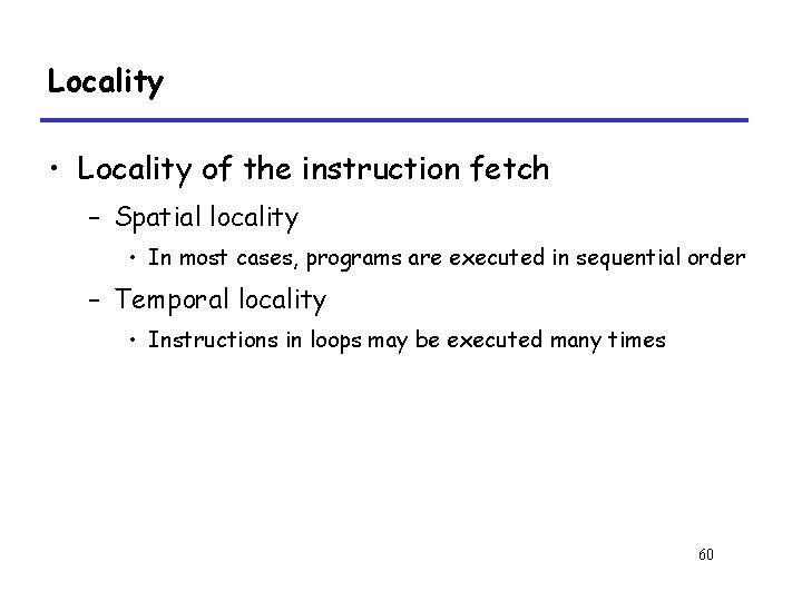
Locality • Locality of the instruction fetch – Spatial locality • In most cases, programs are executed in sequential order – Temporal locality • Instructions in loops may be executed many times 60

6. 3 Memory Hierarchy 61

Memory Hierarchy • Fundamental properties of storage technology and computer software – Different storage technologies have widely different access times – Faster technologies cost more per byte than slower ones and have less capacity – The gap between CPU and main memory speed is widening – Well-written programs tend to exhibit good locality 62

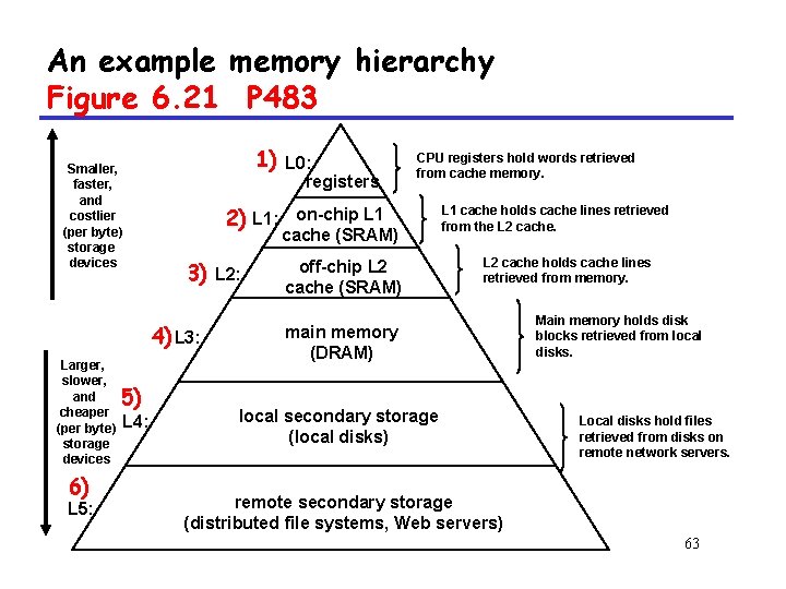
An example memory hierarchy Figure 6. 21 P 483 Smaller, faster, and costlier (per byte) storage devices 1) 2) L 1: 3) 4) L 3: Larger, slower, and cheaper (per byte) storage devices 6) L 5: 5) L 4: L 2: L 0: registers CPU registers hold words retrieved from cache memory. on-chip L 1 cache (SRAM) off-chip L 2 cache (SRAM) L 1 cache holds cache lines retrieved from the L 2 cache holds cache lines retrieved from memory. main memory (DRAM) local secondary storage (local disks) Main memory holds disk blocks retrieved from local disks. Local disks hold files retrieved from disks on remote network servers. remote secondary storage (distributed file systems, Web servers) 63

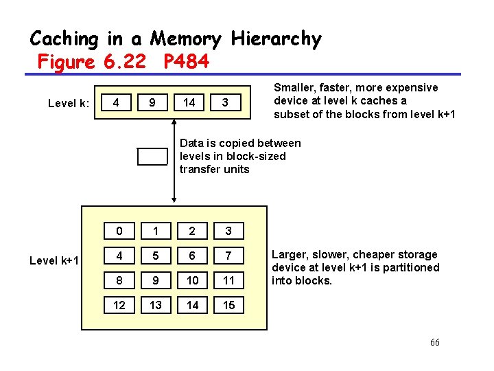
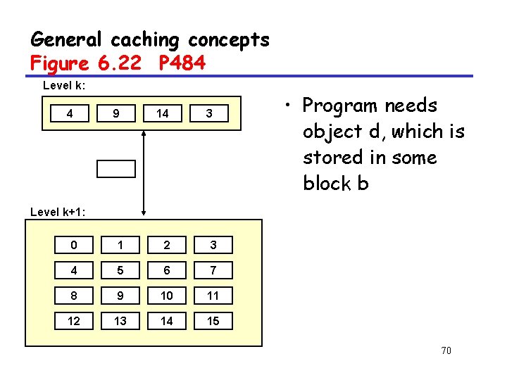
Caching in Memory Hierarchy • Cache – A small, fast device that acts as a staging area for the data objects stored in a large, slower device • Caching – Process of using a cache 64

Caching in Memory Hierarchy • In a memory hierarchy – For each k, – the faster and smaller storage device at level k – serves as a cache for – the larger and slower storage device at level k+1 65

Caching in a Memory Hierarchy Figure 6. 22 P 484 Level k: 4 9 14 3 Smaller, faster, more expensive device at level k caches a subset of the blocks from level k+1 Data is copied between levels in block-sized transfer units Level k+1: 0 1 2 3 4 5 6 7 8 9 10 11 12 13 14 15 Larger, slower, cheaper storage device at level k+1 is partitioned into blocks. 66

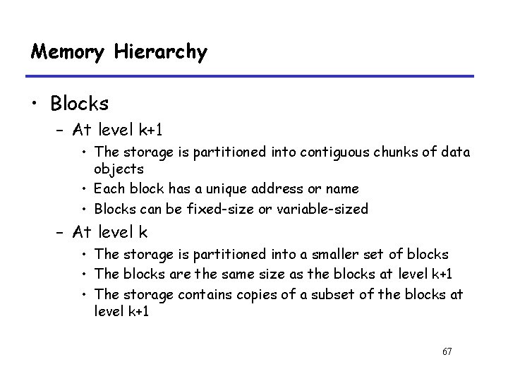
Memory Hierarchy • Blocks – At level k+1 • The storage is partitioned into contiguous chunks of data objects • Each block has a unique address or name • Blocks can be fixed-size or variable-sized – At level k • The storage is partitioned into a smaller set of blocks • The blocks are the same size as the blocks at level k+1 • The storage contains copies of a subset of the blocks at level k+1 67

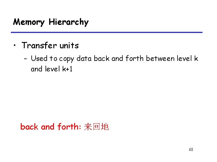
Memory Hierarchy • Transfer units – Used to copy data back and forth between level k and level k+1 back and forth: 来回地 68

Memory Locality • For any pair of adjacent levels, the block size is fixed • For other pairs of adjacent levels, the block can have different size 69

General caching concepts Figure 6. 22 P 484 Level k: 4 9 14 3 • Program needs object d, which is stored in some block b Level k+1: 0 1 2 3 4 5 6 7 8 9 10 11 12 13 14 15 70

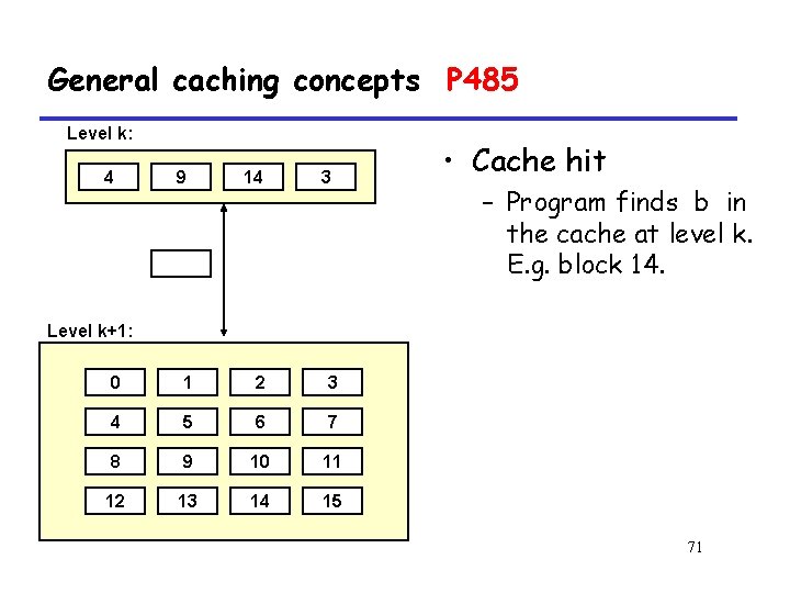
General caching concepts P 485 Level k: 4 9 14 3 • Cache hit – Program finds b in the cache at level k. E. g. block 14. Level k+1: 0 1 2 3 4 5 6 7 8 9 10 11 12 13 14 15 71

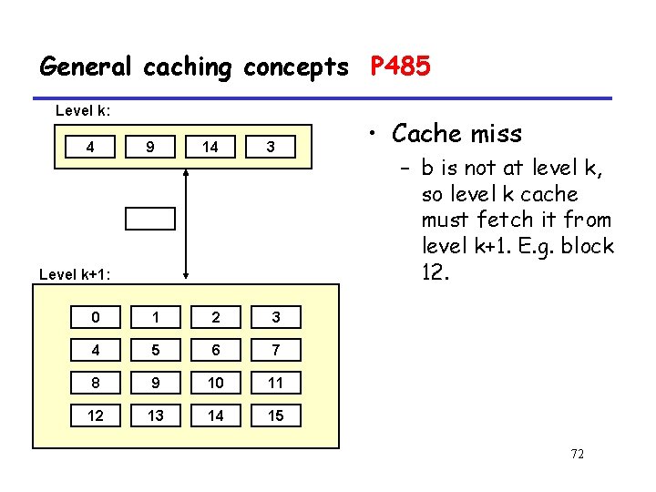
General caching concepts P 485 Level k: 4 9 14 3 Level k+1: 0 1 2 3 4 5 6 7 8 9 10 11 12 13 14 15 • Cache miss – b is not at level k, so level k cache must fetch it from level k+1. E. g. block 12. 72

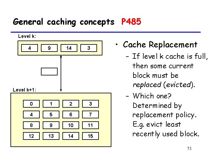
General caching concepts P 485 Level k: 4 9 14 3 • Cache Replacement – If level k cache is full, then some current block must be replaced (evicted). Level k+1: 0 1 2 3 4 5 6 7 8 9 10 11 12 13 14 15 – Which one? Determined by replacement policy. E. g. evict least recently used block. 73

Types of Cache Misses • 1)Cold (compulsory) miss – Cold misses occur because the cache is empty. 74

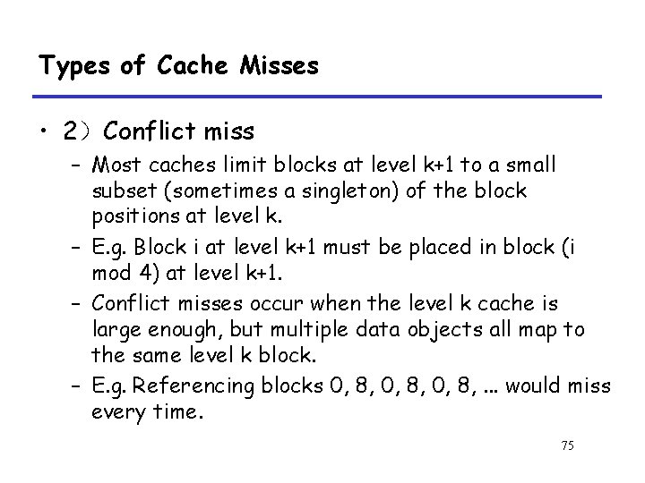
Types of Cache Misses • 2)Conflict miss – Most caches limit blocks at level k+1 to a small subset (sometimes a singleton) of the block positions at level k. – E. g. Block i at level k+1 must be placed in block (i mod 4) at level k+1. – Conflict misses occur when the level k cache is large enough, but multiple data objects all map to the same level k block. – E. g. Referencing blocks 0, 8, . . . would miss every time. 75

Types of Cache Misses • 3)Capacity miss – Occurs when the set of active cache blocks (working set) is larger than the cache. 76

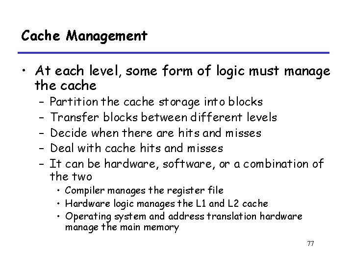
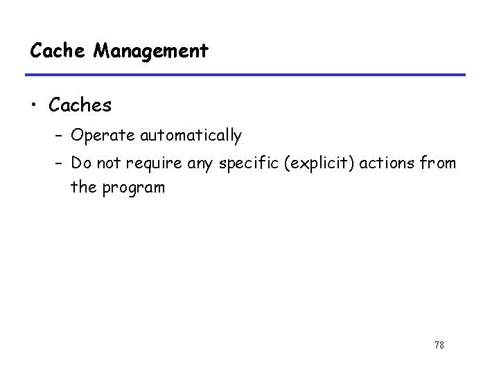
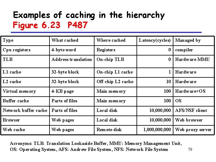
Cache Management • At each level, some form of logic must manage the cache – – – Partition the cache storage into blocks Transfer blocks between different levels Decide when there are hits and misses Deal with cache hits and misses It can be hardware, software, or a combination of the two • Compiler manages the register file • Hardware logic manages the L 1 and L 2 cache • Operating system and address translation hardware manage the main memory 77

Cache Management • Caches – Operate automatically – Do not require any specific (explicit) actions from the program 78

Examples of caching in the hierarchy Figure 6. 23 P 487 Type What cached Where cached Latency(cycles) Managed by Cpu registers 4 -byte word Registers TLB Address translation On-chip TLB 0 Hardware MMU L 1 cache 32 -byte block On-chip L 1 cache 1 Hardware L 2 cache 32 -byte block Off-chip L 2 cache 10 Hardware Virtual memory 4 -KB page Main memory 100 Hardware+OS Buffer cache Parts of files Main memory 100 OS 0 compiler Network buffer cache Parts of files Local disk 10, 000 AFS/NSF client Browser Web pages Local disk 10, 000 Web browser Web cache Web pages Remote disk 1, 000, 000 Web proxy server Acronyms: TLB: Translation Lookaside Buffer, MMU: Memory Management Unit, OS: Operating System, AFS: Andrew File System, NFS: Network File System 79