Memory Elements SRAMs DRAMs Recap of RISCV Addressing

![SRAM Din[1] e. g. How do we design a 4 x 2 SRAM Module? SRAM Din[1] e. g. How do we design a 4 x 2 SRAM Module?](https://slidetodoc.com/presentation_image_h2/aff64dcc884fe1e9abc1ff9c07de367e/image-12.jpg)
![Bit Lines SRAM Din[1] e. g. How do we design a 4 x 2 Bit Lines SRAM Din[1] e. g. How do we design a 4 x 2](https://slidetodoc.com/presentation_image_h2/aff64dcc884fe1e9abc1ff9c07de367e/image-13.jpg)

- Slides: 28

Memory Elements -- SRAMs, DRAMs Recap of RISC-V Addressing CS 3432 Fall 2020 Shirley Moore, Instructor svmoore@utep. edu October 29, 2020 1

Schedule for Today’s Class • Announcements • Make appointments to discuss midterm exam at https: //calendly. com/svmoore (choose 15 or 30 minute appointment) • Midterm retakes will be ready by mid to end of next week • In 3 parts, set aside 1 hour for each part, you must start and finish a part in one sitting • Can do 1, 2, or all 3 parts • Dropping and S/U grades • I will add lab 1 grades to Black. Board and redo weight total • Memory Design (30 minutes) • P&H A. 9 • Recap of RISC-V Addressing (30 minutes) • Wrapup • Memory Design Homework • Preview of Lab 4 2

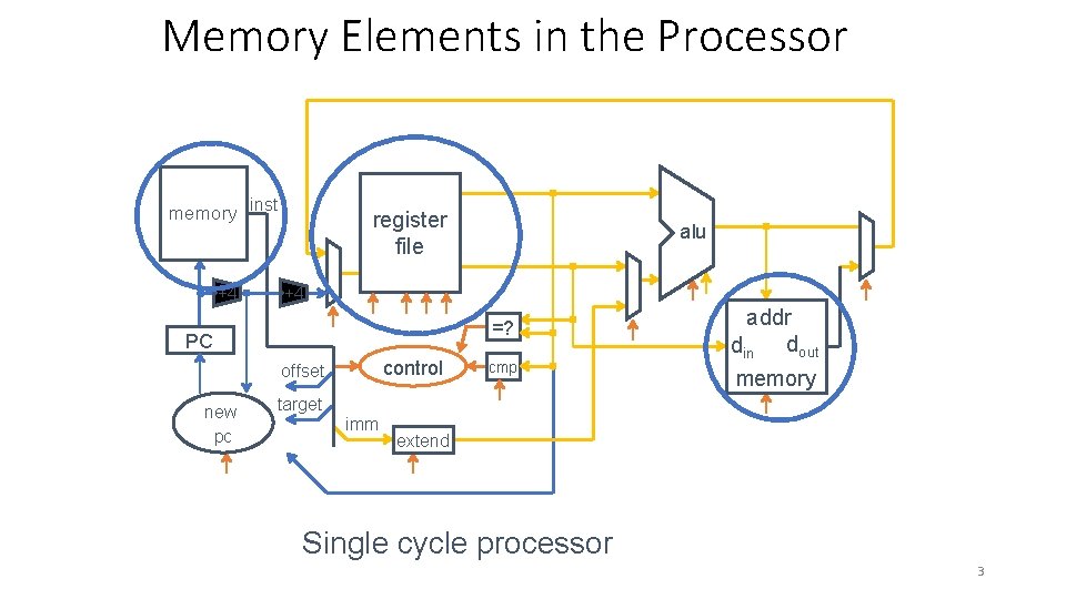
Memory Elements in the Processor memory inst +4 register file +4 =? PC control offset new pc alu cmp addr din dout memory target imm extend Single cycle processor 3

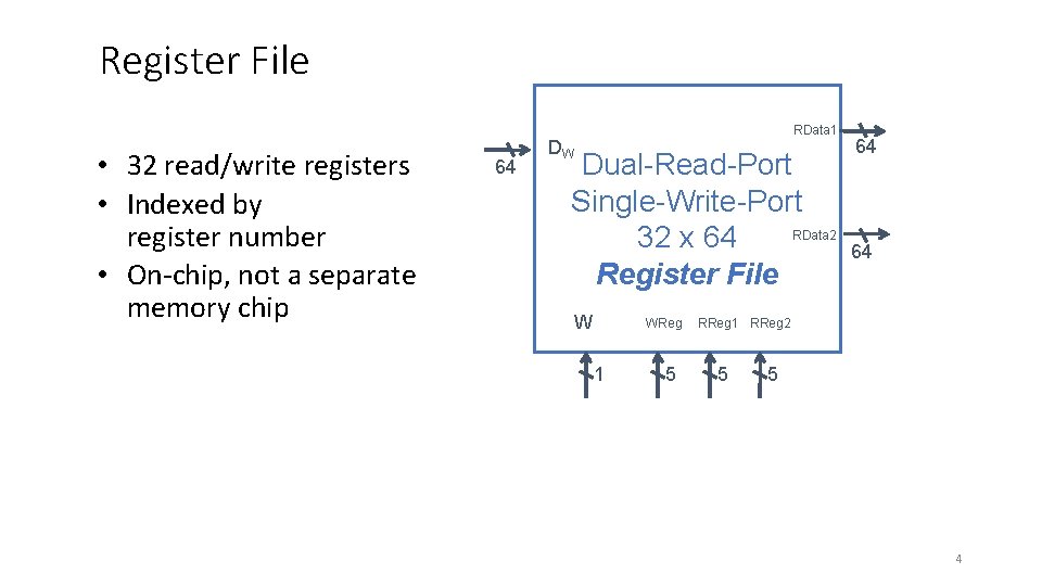
Register File • 32 read/write registers • Indexed by register number • On-chip, not a separate memory chip 64 RData 1 DW Dual-Read-Port Single-Write-Port RData 2 32 x 64 Register File W WReg 1 5 64 64 RReg 1 RReg 2 5 5 4

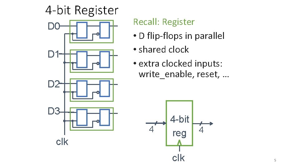
4 -bit Register D 0 D 1 D 2 Recall: Register • D flip-flops in parallel • shared clock • extra clocked inputs: write_enable, reset, … D 3 4 clk 4 -bit reg 4 clk 5

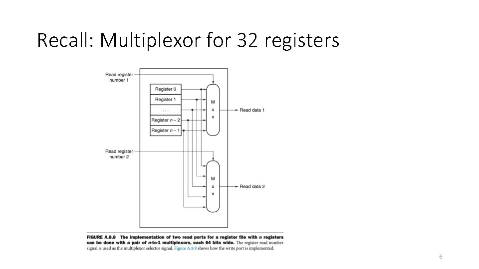
Recall: Multiplexor for 32 registers 6

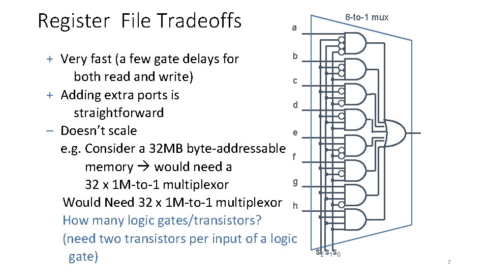
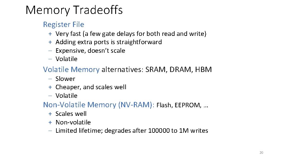
Register File Tradeoffs 8 -to-1 mux a b + Very fast (a few gate delays for both read and write) c + Adding extra ports is d straightforward – Doesn’t scale e e. g. Consider a 32 MB byte-addressable f memory would need a g 32 x 1 M-to-1 multiplexor Would Need 32 x 1 M-to-1 multiplexor h How many logic gates/transistors? (need two transistors per input of a logic gate) s 2 s 1 s 0 7

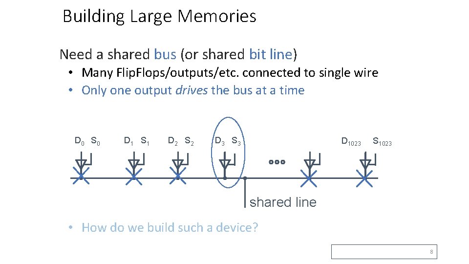
Building Large Memories Need a shared bus (or shared bit line) • Many Flip. Flops/outputs/etc. connected to single wire • Only one output drives the bus at a time D 0 S 0 D 1 S 1 D 2 S 2 D 3 S 3 D 1023 S 1023 shared line • How do we build such a device? 8

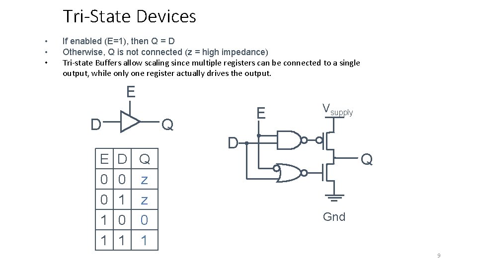
Tri-State Devices • • • If enabled (E=1), then Q = D Otherwise, Q is not connected (z = high impedance) Tri-state Buffers allow scaling since multiple registers can be connected to a single output, while only one register actually drives the output. E D E 0 0 1 1 E Q D 0 1 Q z z 0 1 Vsupply D Q Gnd 9

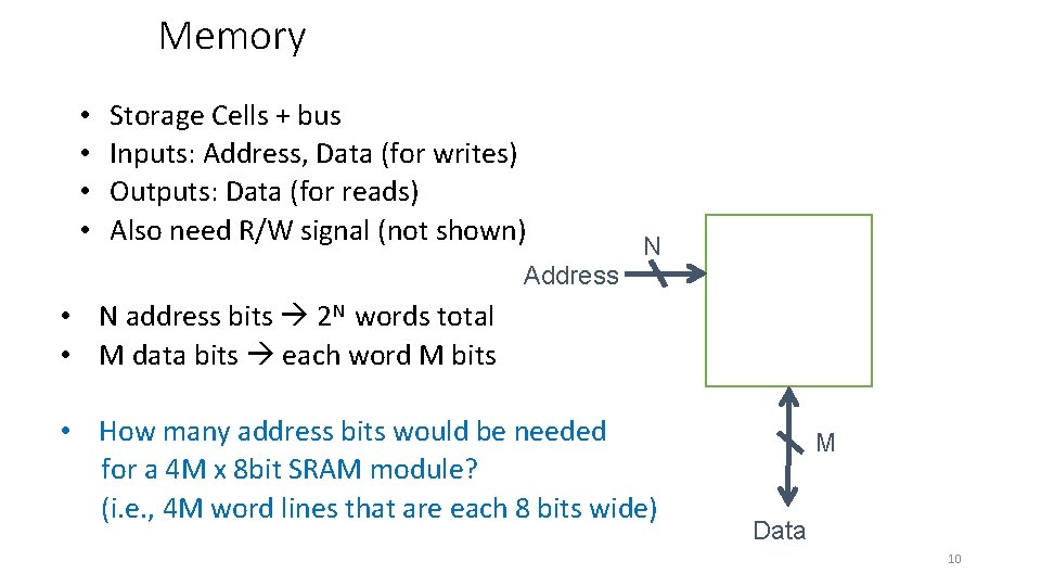
Memory • • Storage Cells + bus Inputs: Address, Data (for writes) Outputs: Data (for reads) Also need R/W signal (not shown) N Address • N address bits 2 N words total • M data bits each word M bits • How many address bits would be needed for a 4 M x 8 bit SRAM module? (i. e. , 4 M word lines that are each 8 bits wide) M Data 10

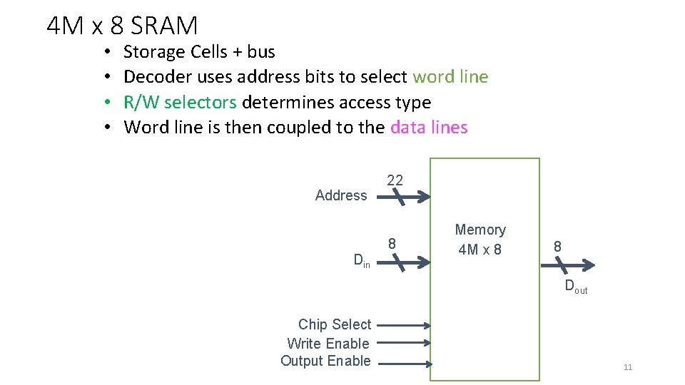
4 M x 8 SRAM • • Storage Cells + bus Decoder uses address bits to select word line R/W selectors determines access type Word line is then coupled to the data lines Address Din 22 8 Memory 4 M x 8 8 Dout Chip Select Write Enable Output Enable 11
![SRAM Din1 e g How do we design a 4 x 2 SRAM Module SRAM Din[1] e. g. How do we design a 4 x 2 SRAM Module?](https://slidetodoc.com/presentation_image_h2/aff64dcc884fe1e9abc1ff9c07de367e/image-12.jpg)
SRAM Din[1] e. g. How do we design a 4 x 2 SRAM Module? Din[2] D Q D Q enable 0 (i. e. 4 word lines that are each 2 bits wide)? 2 -to-4 decoder 1 2 Address Q 4 x 2 DSRAM D Q enable 2 3 Write Enable Output Enable Dout[1] Dout[2] 12
![Bit Lines SRAM Din1 e g How do we design a 4 x 2 Bit Lines SRAM Din[1] e. g. How do we design a 4 x 2](https://slidetodoc.com/presentation_image_h2/aff64dcc884fe1e9abc1ff9c07de367e/image-13.jpg)
Bit Lines SRAM Din[1] e. g. How do we design a 4 x 2 SRAM Module? Din[2] D Q D Q enable enable 0 (i. e. 4 word lines that are each 2 bits wide)? 2 -to-4 decoder 1 2 Address Word lines 2 3 Write Enable Output Enable Dout[1] Dout[2] 13

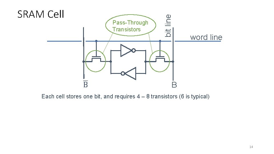
Pass-Through Transistors bit line SRAM Cell word line B Each cell stores one bit, and requires 4 – 8 transistors (6 is typical) 14

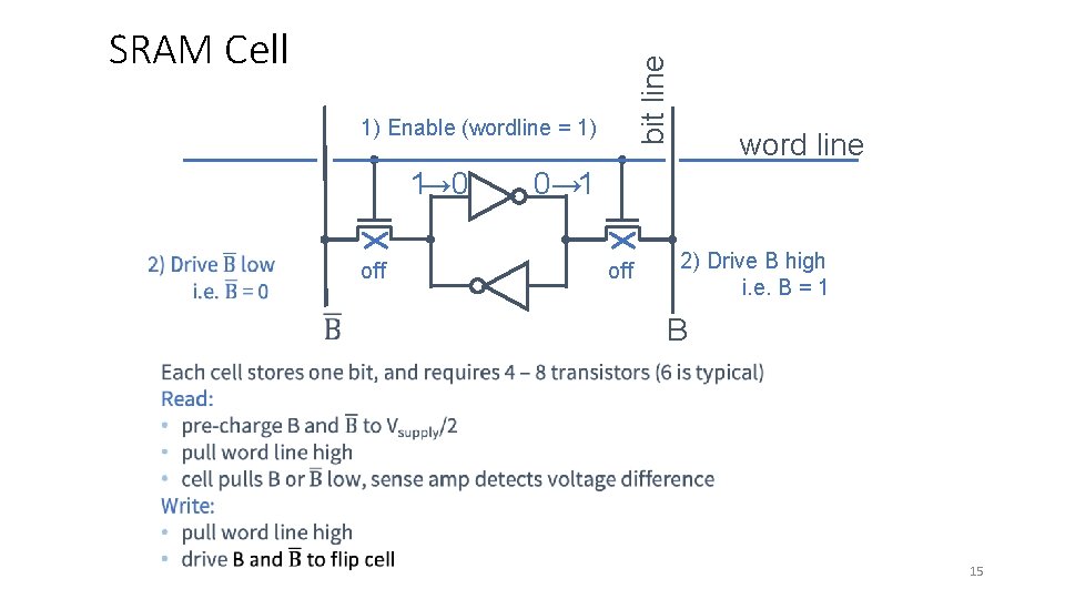
bit line SRAM Cell 1) Enable(wordline==0) 1) Disabled 1→ 0 off on word line 0→ 1 off on 2) Drive B high i. e. B = 1 B 15

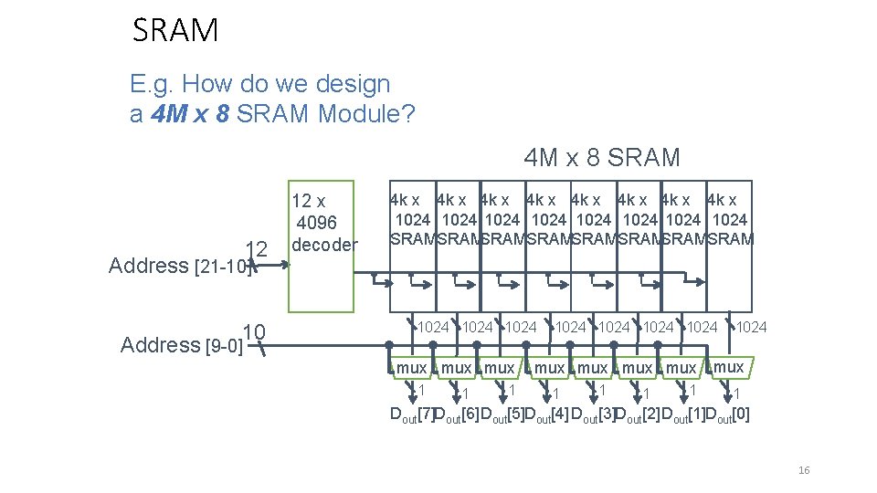
SRAM E. g. How do we design a 4 M x 8 SRAM Module? 4 M x 8 SRAM 12 Address [21 -10] 10 Address [9 -0] 12 x 4096 decoder 4 k x 4 k x 1024 1024 SRAMSRAMSRAMSRAM 1024 mux mux 1 1024 1024 mux mux mux 1 1 1 Dout[7]Dout[6] Dout[5]Dout[4] Dout[3]Dout[2] Dout[1]Dout[0] 16

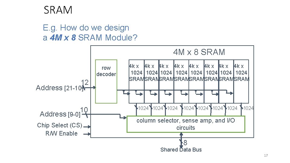
SRAM E. g. How do we design a 4 M x 8 SRAM Module? 4 M x 8 SRAM row decoder 12 4 k x 4 k x 1024 1024 SRAMSRAMSRAMSRAM Address [21 -10] 10 Address [9 -0] Chip Select (CS) R/W Enable 1024 1024 column selector, sense amp, and I/O circuits 8 Shared Data Bus 17

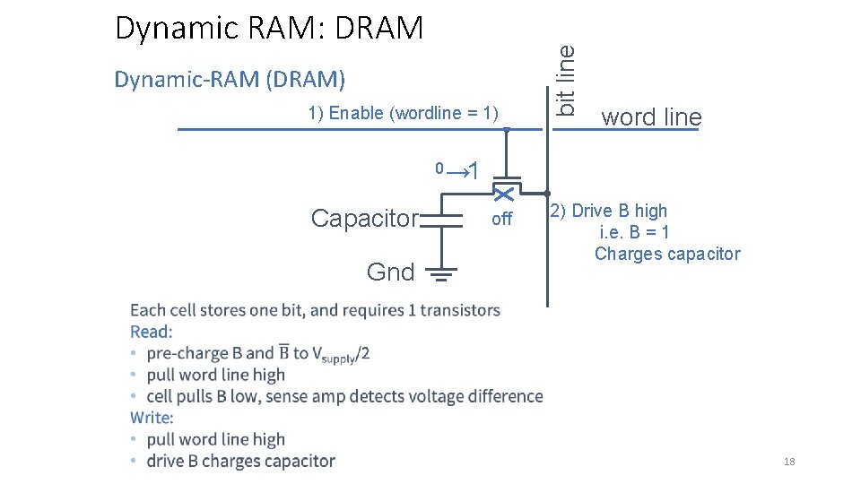
Dynamic-RAM (DRAM) 1)Disable Enable (wordline == 0) 1) bit line Dynamic RAM: DRAM word line 0 → 1 Capacitor Gnd on off 2) Drive B high i. e. B = 1 Charges capacitor 18

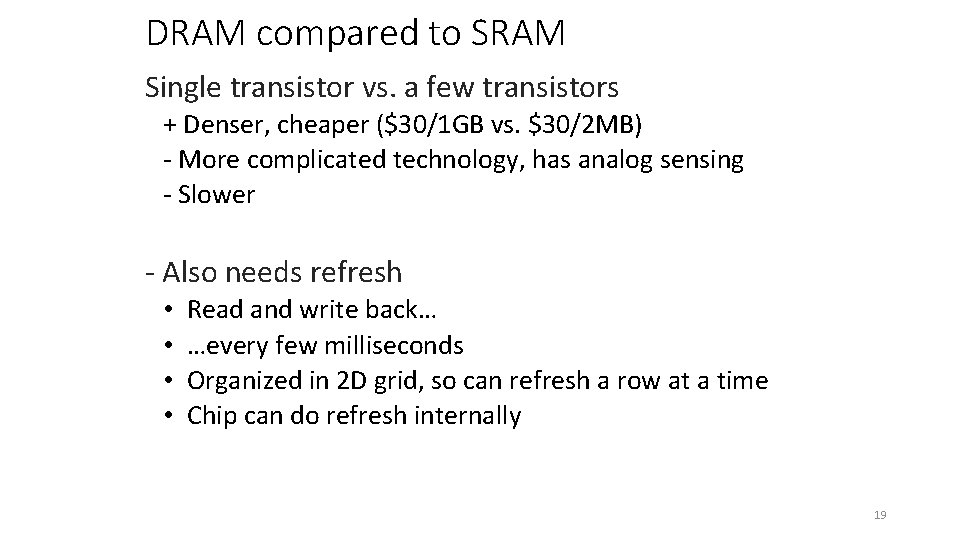
DRAM compared to SRAM Single transistor vs. a few transistors + Denser, cheaper ($30/1 GB vs. $30/2 MB) - More complicated technology, has analog sensing - Slower - Also needs refresh • • Read and write back… …every few milliseconds Organized in 2 D grid, so can refresh a row at a time Chip can do refresh internally 19

Memory Tradeoffs Register File + + – – Very fast (a few gate delays for both read and write) Adding extra ports is straightforward Expensive, doesn’t scale Volatile Memory alternatives: SRAM, DRAM, HBM – Slower + Cheaper, and scales well – Volatile Non-Volatile Memory (NV-RAM): Flash, EEPROM, … + Scales well + Non-volatile – Limited lifetime; degrades after 100000 to 1 M writes 20

Memory Element in Logisim • Memory/RAM • See documentation at http: //www. cburch. com/logisim/docs/2. 3. 0/libs/mem/ram. html 21

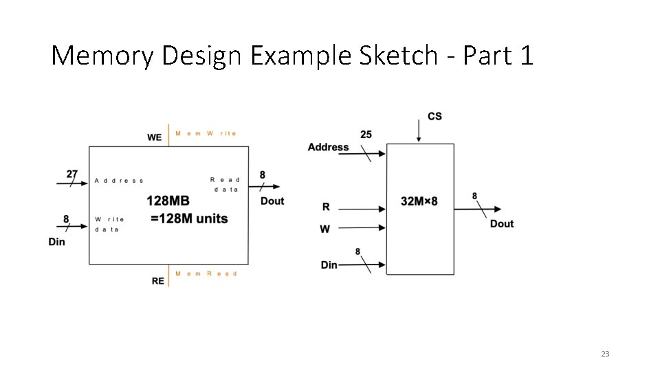
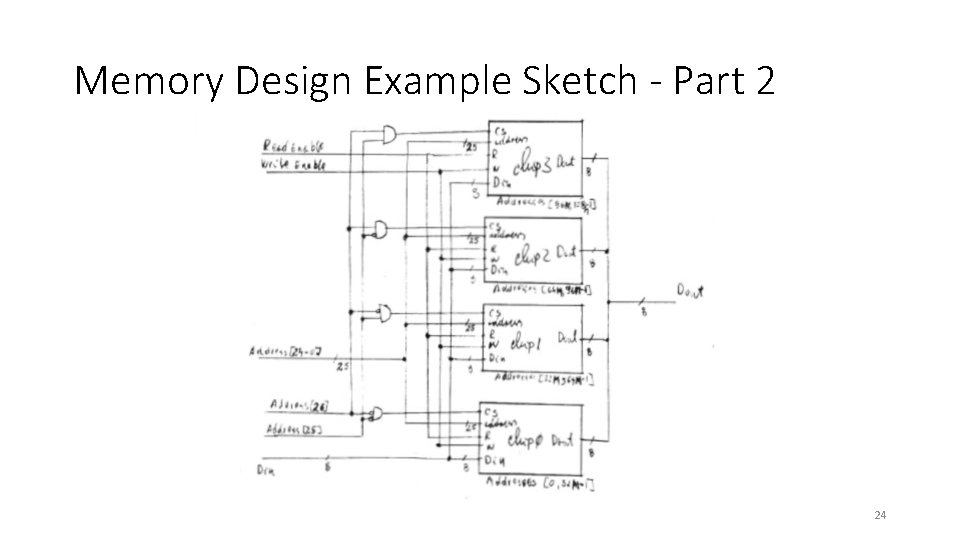
Memory Design Example • Design a 128 Mbyte memory using 32 M*8 chips, with 8 -bit read/write operations and byte addressability. • Suggestion: Sketch first on paper, then use Logisim 22

Memory Design Example Sketch - Part 1 23

Memory Design Example Sketch - Part 2 24

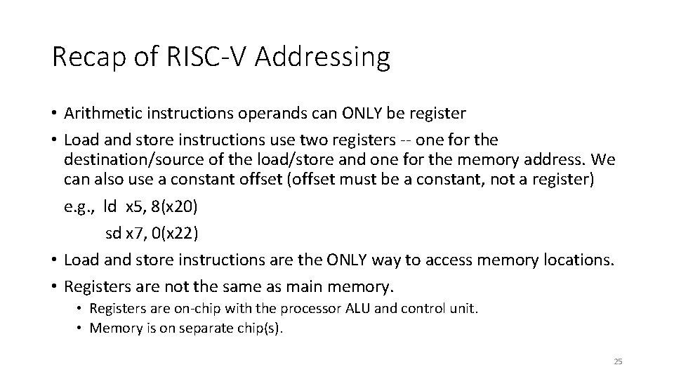
Recap of RISC-V Addressing • Arithmetic instructions operands can ONLY be register • Load and store instructions use two registers -- one for the destination/source of the load/store and one for the memory address. We can also use a constant offset (offset must be a constant, not a register) e. g. , ld x 5, 8(x 20) sd x 7, 0(x 22) • Load and store instructions are the ONLY way to access memory locations. • Registers are not the same as main memory. • Registers are on-chip with the processor ALU and control unit. • Memory is on separate chip(s). 25

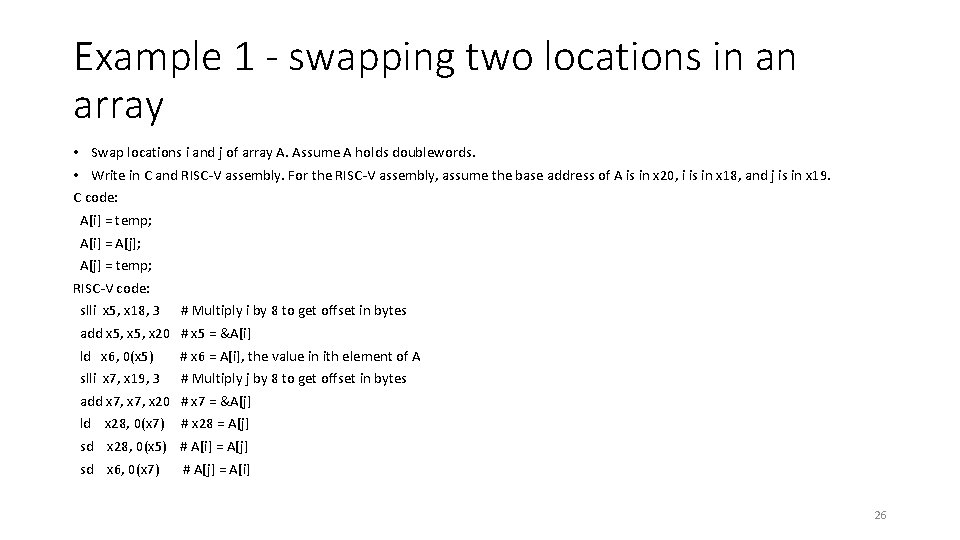
Example 1 - swapping two locations in an array • Swap locations i and j of array A. Assume A holds doublewords. • Write in C and RISC-V assembly. For the RISC-V assembly, assume the base address of A is in x 20, i is in x 18, and j is in x 19. C code: A[i] = temp; A[i] = A[j]; A[j] = temp; RISC-V code: slli x 5, x 18, 3 # Multiply i by 8 to get offset in bytes add x 5, x 20 # x 5 = &A[i] ld x 6, 0(x 5) # x 6 = A[i], the value in ith element of A slli x 7, x 19, 3 # Multiply j by 8 to get offset in bytes add x 7, x 20 # x 7 = &A[j] ld x 28, 0(x 7) # x 28 = A[j] sd x 28, 0(x 5) # A[i] = A[j] sd x 6, 0(x 7) # A[j] = A[i] 26

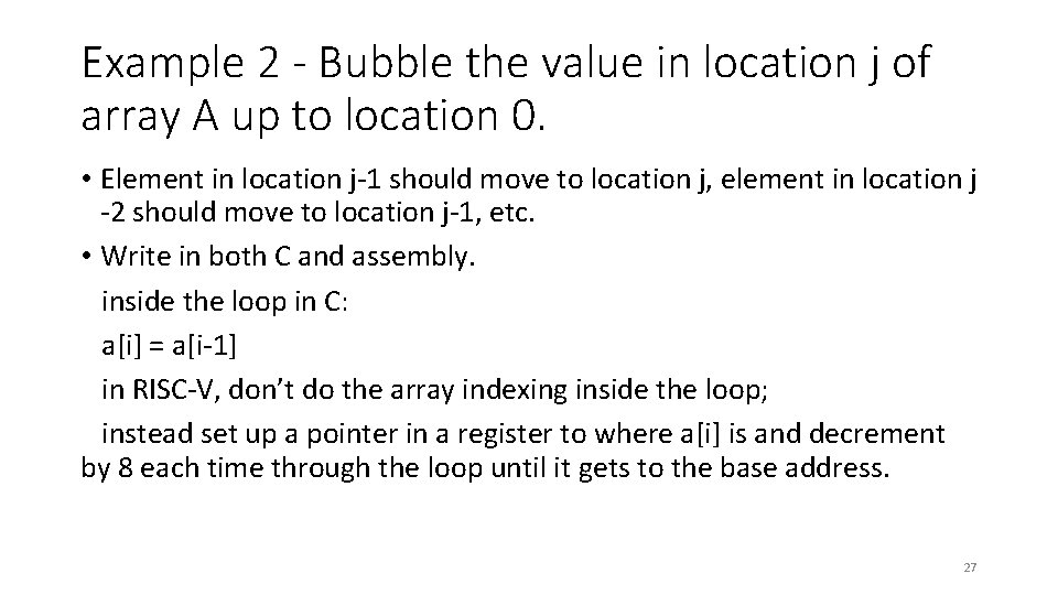
Example 2 - Bubble the value in location j of array A up to location 0. • Element in location j-1 should move to location j, element in location j -2 should move to location j-1, etc. • Write in both C and assembly. inside the loop in C: a[i] = a[i-1] in RISC-V, don’t do the array indexing inside the loop; instead set up a pointer in a register to where a[i] is and decrement by 8 each time through the loop until it gets to the base address. 27

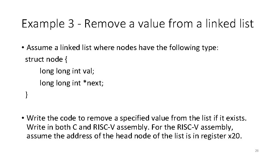
Example 3 - Remove a value from a linked list • Assume a linked list where nodes have the following type: struct node { long int val; long int *next; } • Write the code to remove a specified value from the list if it exists. Write in both C and RISC-V assembly. For the RISC-V assembly, assume the address of the head node of the list is in register x 20. 28