Memory and Programmable Logic EE 200 Digital Logic
Memory and Programmable Logic EE 200 Digital Logic Circuit Design Dr. Muhamed Mudawar King Fahd University of Petroleum and Minerals
Presentation Outline v Random Access Memory (RAM) v Read-Only Memory (ROM) v Programmable Logic Device (PLD) v Programmable Logic Array (PLA) v Programmable Array Logic (PAL) Memory and Programmable Logic EE 200 – Digital Logic Circuit Design © Muhamed Mudawar – slide 2
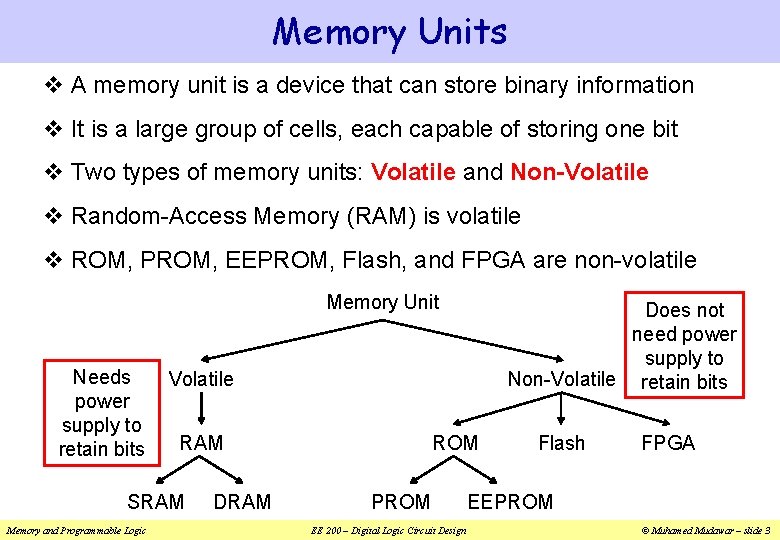
Memory Units v A memory unit is a device that can store binary information v It is a large group of cells, each capable of storing one bit v Two types of memory units: Volatile and Non-Volatile v Random-Access Memory (RAM) is volatile v ROM, PROM, EEPROM, Flash, and FPGA are non-volatile Memory Unit Needs power supply to retain bits Volatile RAM SRAM Memory and Programmable Logic Does not need power supply to Non-Volatile retain bits DRAM ROM PROM EE 200 – Digital Logic Circuit Design Flash FPGA EEPROM © Muhamed Mudawar – slide 3
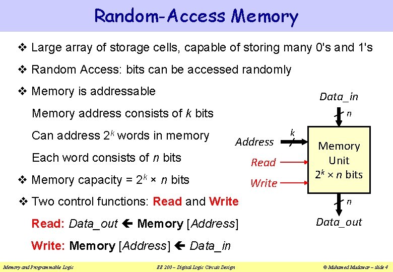
Random-Access Memory v Large array of storage cells, capable of storing many 0's and 1's v Random Access: bits can be accessed randomly v Memory is addressable Data_in Memory address consists of k bits Can address 2 k words in memory n Address Each word consists of n bits Read v Memory capacity = 2 k × n bits Write v Two control functions: Read and Write Read: Data_out Memory [Address] k Memory Unit 2 k × n bits n Data_out Write: Memory [Address] Data_in Memory and Programmable Logic EE 200 – Digital Logic Circuit Design © Muhamed Mudawar – slide 4
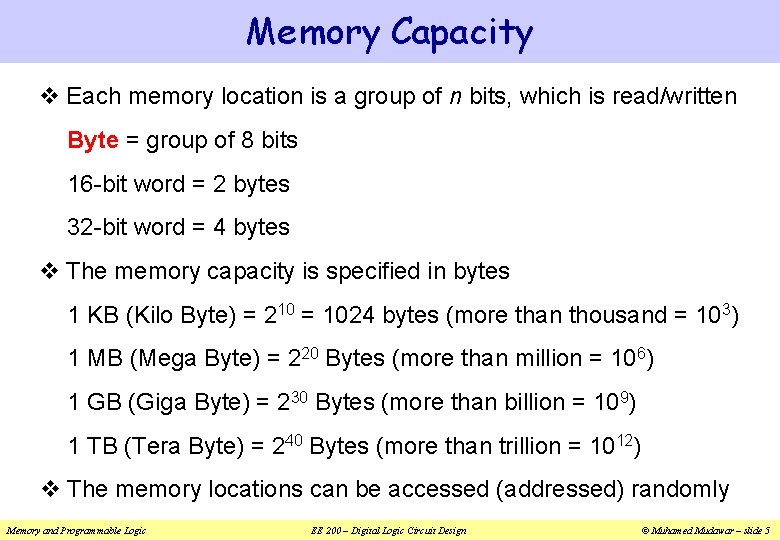
Memory Capacity v Each memory location is a group of n bits, which is read/written Byte = group of 8 bits 16 -bit word = 2 bytes 32 -bit word = 4 bytes v The memory capacity is specified in bytes 1 KB (Kilo Byte) = 210 = 1024 bytes (more than thousand = 103) 1 MB (Mega Byte) = 220 Bytes (more than million = 106) 1 GB (Giga Byte) = 230 Bytes (more than billion = 109) 1 TB (Tera Byte) = 240 Bytes (more than trillion = 1012) v The memory locations can be accessed (addressed) randomly Memory and Programmable Logic EE 200 – Digital Logic Circuit Design © Muhamed Mudawar – slide 5
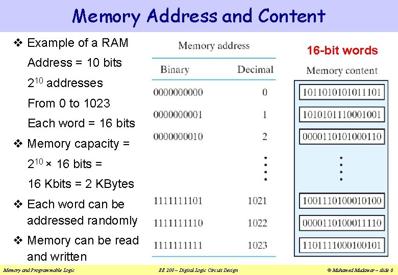
Memory Address and Content v Example of a RAM 16 -bit words Address = 10 bits 210 addresses From 0 to 1023 Each word = 16 bits v Memory capacity = 210 × 16 bits = 16 Kbits = 2 KBytes v Each word can be addressed randomly v Memory can be read and written Memory and Programmable Logic EE 200 – Digital Logic Circuit Design © Muhamed Mudawar – slide 6
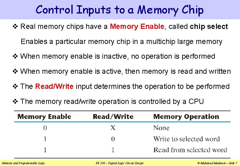
Control Inputs to a Memory Chip v Real memory chips have a Memory Enable, called chip select Enables a particular memory chip in a multichip large memory v When memory enable is inactive, no operation is performed v When memory enable is active, then memory is read and written v The Read/Write input determines the operation to be performed v The memory read/write operation is controlled by a CPU Memory and Programmable Logic EE 200 – Digital Logic Circuit Design © Muhamed Mudawar – slide 7
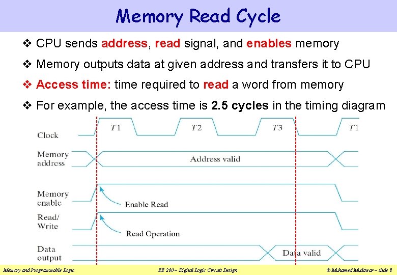
Memory Read Cycle v CPU sends address, read signal, and enables memory v Memory outputs data at given address and transfers it to CPU v Access time: time required to read a word from memory v For example, the access time is 2. 5 cycles in the timing diagram Memory and Programmable Logic EE 200 – Digital Logic Circuit Design © Muhamed Mudawar – slide 8
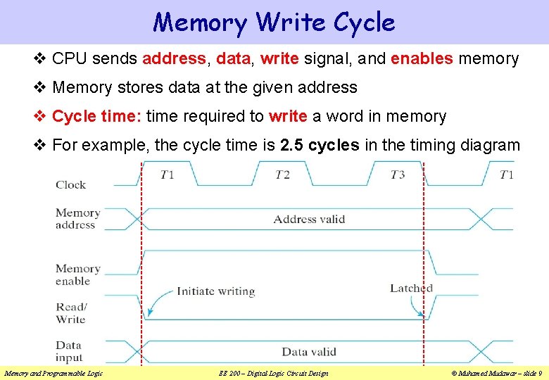
Memory Write Cycle v CPU sends address, data, write signal, and enables memory v Memory stores data at the given address v Cycle time: time required to write a word in memory v For example, the cycle time is 2. 5 cycles in the timing diagram Memory and Programmable Logic EE 200 – Digital Logic Circuit Design © Muhamed Mudawar – slide 9
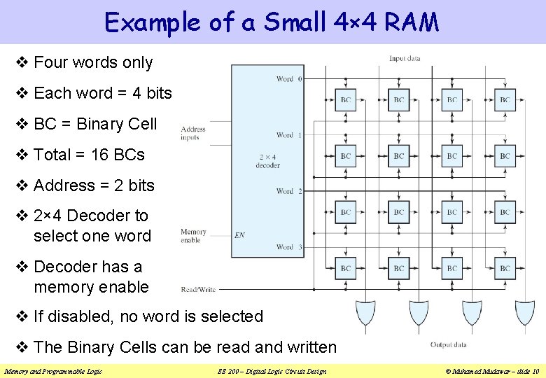
Example of a Small 4× 4 RAM v Four words only v Each word = 4 bits v BC = Binary Cell v Total = 16 BCs v Address = 2 bits v 2× 4 Decoder to select one word v Decoder has a memory enable v If disabled, no word is selected v The Binary Cells can be read and written Memory and Programmable Logic EE 200 – Digital Logic Circuit Design © Muhamed Mudawar – slide 10
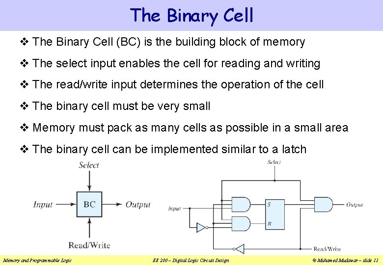
The Binary Cell v The Binary Cell (BC) is the building block of memory v The select input enables the cell for reading and writing v The read/write input determines the operation of the cell v The binary cell must be very small v Memory must pack as many cells as possible in a small area v The binary cell can be implemented similar to a latch Memory and Programmable Logic EE 200 – Digital Logic Circuit Design © Muhamed Mudawar – slide 11
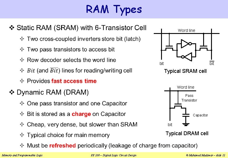
RAM Types v Word line bit Typical SRAM cell Word line Pass Transistor Capacitor bit Typical DRAM cell Memory and Programmable Logic EE 200 – Digital Logic Circuit Design © Muhamed Mudawar – slide 12
Memory Address Decoding v A decoder with k address inputs has 2 k outputs v It requires 2 k AND gates, each having k inputs v The cost of the decoder becomes very large for large memories v To reduce the cost of the address decoder … A two-dimensional memory array is used The memory address is split into row and column addresses Two decoders are used, each having k/2 inputs (address lines) 1. First one decodes the row address to select a row 2. Second one decodes the column address to select a word v A decoder with k/2 inputs requires 2 k/2 AND (much smaller) Memory and Programmable Logic EE 200 – Digital Logic Circuit Design © Muhamed Mudawar – slide 13
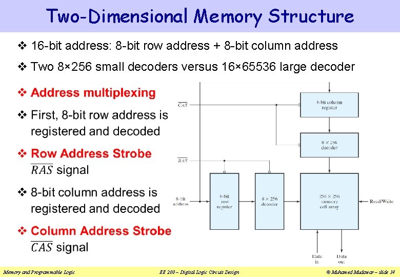
Two-Dimensional Memory Structure v 16 -bit address: 8 -bit row address + 8 -bit column address v Two 8× 256 small decoders versus 16× 65536 large decoder Memory and Programmable Logic EE 200 – Digital Logic Circuit Design © Muhamed Mudawar – slide 14
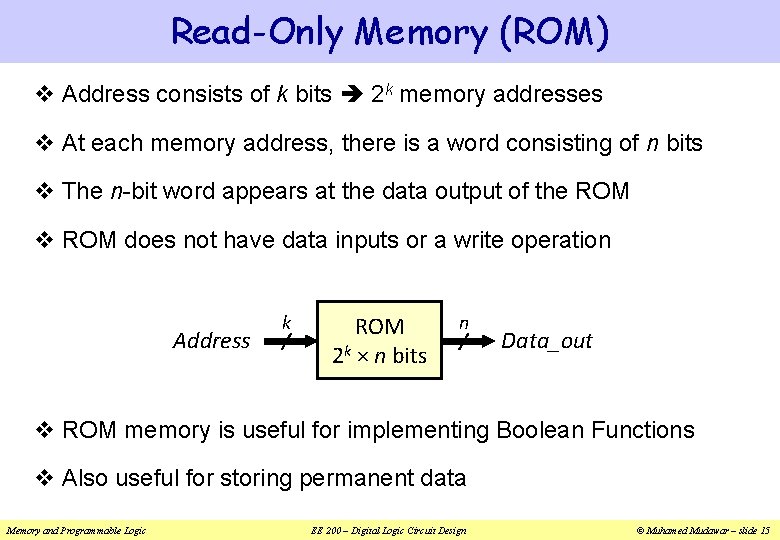
Read-Only Memory (ROM) v Address consists of k bits 2 k memory addresses v At each memory address, there is a word consisting of n bits v The n-bit word appears at the data output of the ROM v ROM does not have data inputs or a write operation Address k ROM 2 k × n bits n Data_out v ROM memory is useful for implementing Boolean Functions v Also useful for storing permanent data Memory and Programmable Logic EE 200 – Digital Logic Circuit Design © Muhamed Mudawar – slide 15
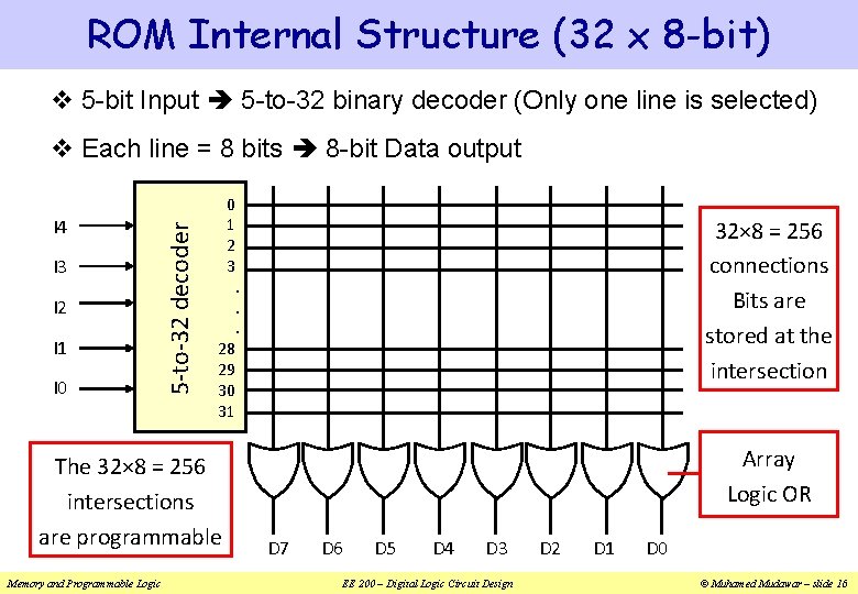
ROM Internal Structure (32 x 8 -bit) v 5 -bit Input 5 -to-32 binary decoder (Only one line is selected) I 4 I 3 I 2 I 1 I 0 5 -to-32 decoder v Each line = 8 bits 8 -bit Data output 0 1 2 3 28 29 30 31 The 32× 8 = 256 intersections are programmable Memory and Programmable Logic 32× 8 = 256 connections Bits are stored at the intersection . . . Array Logic OR D 7 D 6 D 5 D 4 D 3 EE 200 – Digital Logic Circuit Design D 2 D 1 D 0 © Muhamed Mudawar – slide 16
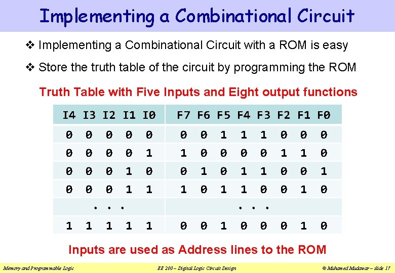
Implementing a Combinational Circuit v Implementing a Combinational Circuit with a ROM is easy v Store the truth table of the circuit by programming the ROM Truth Table with Five Inputs and Eight output functions I 4 I 3 I 2 I 1 I 0 F 7 F 6 F 5 F 4 F 3 F 2 F 1 F 0 0 0 0 0 1 0 0 1 0 0 0 1 · · · 1 1 1 0 0 1 1 0 1 0 0 0 1 1 0 0 · · · 1 0 0 0 1 0 Inputs are used as Address lines to the ROM Memory and Programmable Logic EE 200 – Digital Logic Circuit Design © Muhamed Mudawar – slide 17
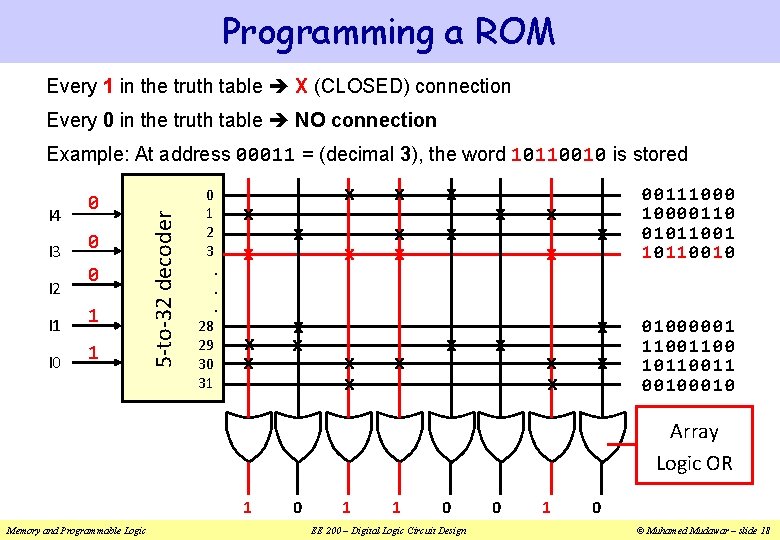
Programming a ROM Every 1 in the truth table X (CLOSED) connection Every 0 in the truth table NO connection I 4 I 3 I 2 0 0 0 I 1 1 I 0 1 5 -to-32 decoder Example: At address 00011 = (decimal 3), the word 10110010 is stored 0 1 2 3 28 29 30 31 x. . . x x x x x x x 001110000110 010110010 01000001 1100 10110011 0010 Array Logic OR 1 Memory and Programmable Logic 0 1 1 0 EE 200 – Digital Logic Circuit Design 0 1 0 © Muhamed Mudawar – slide 18
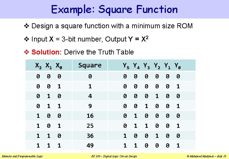
Example: Square Function v Design a square function with a minimum size ROM v Input X = 3 -bit number, Output Y = X 2 v Solution: Derive the Truth Table X 2 X 1 X 0 Square Y 5 Y 4 Y 3 Y 2 Y 1 Y 0 0 0 0 1 1 0 0 0 1 0 4 0 0 0 1 1 9 0 0 1 1 0 0 16 0 1 0 1 25 0 1 1 0 0 1 1 1 0 36 1 0 0 1 1 1 49 1 1 0 0 0 1 Memory and Programmable Logic EE 200 – Digital Logic Circuit Design © Muhamed Mudawar – slide 19
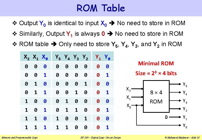
ROM Table v Output Y 0 is identical to input X 0 No need to store in ROM v Similarly, Output Y 1 is always 0 No need to store in ROM v ROM table Only need to store Y 5, Y 4, Y 3, and Y 2 in ROM X 2 X 1 X 0 Y 5 Y 4 Y 3 Y 2 Y 1 Y 0 0 0 1 0 0 0 1 0 0 0 1 1 0 0 0 0 1 0 1 1 0 0 1 0 0 1 1 1 0 0 0 1 Memory and Programmable Logic EE 200 – Digital Logic Circuit Design Minimal ROM Size = 23 × 4 bits X 2 X 1 X 0 Y 5 8× 4 ROM Y 4 Y 3 Y 2 0 Y 1 Y 0 © Muhamed Mudawar – slide 20
Types of ROMs v ROM may be programmed in four different ways 1. Mask Programming: done by circuit manufacturer (not by user) 2. Programmable Read-Only Memory (PROM) ² Fuses in the PROM are blown using a high-voltage pulse ² Can be programmed only once (irreversible) 3. Erasable PROM (EPROM) Programming can be erased using ultraviolet light 4. Electrically Erasable PROM (EEPROM) Can be erased with an electric signal instead of ultraviolet light v Flash memory is similar to EEPROMs but has additional circuitry to erase blocks of memory Memory and Programmable Logic EE 200 – Digital Logic Circuit Design © Muhamed Mudawar – slide 21
Programmable Logic Devices (PLDs) v Three major types of Programmable Logic Devices (PLDs) v They differ in the placement of programmable connections 1. Programmable Read-Only Memory (PROM) Fixed AND array (decoder) and programmable OR array 2. Programmable Array Logic (PAL) Programmable AND array and fixed OR array 3. Programmable Logic Array (PLA) is the most flexible Programmable AND array and Programmable OR array Memory and Programmable Logic EE 200 – Digital Logic Circuit Design © Muhamed Mudawar – slide 22
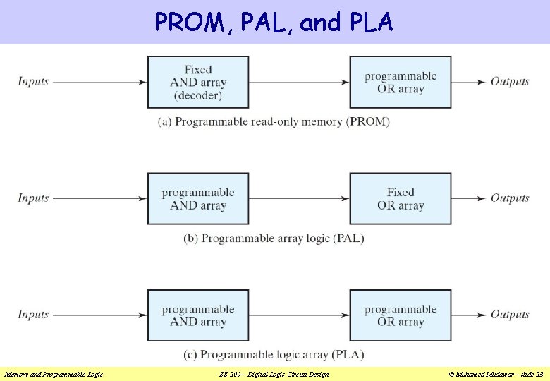
PROM, PAL, and PLA Memory and Programmable Logic EE 200 – Digital Logic Circuit Design © Muhamed Mudawar – slide 23
Programmable Logic Array (PLA) v Similar to PROM, but no decoder v Does NOT generate all minterms v Decoder is replaced by an array of AND gates v Programmable AND array can generate any product term v Product terms are passed to a programmable OR array v Programmable OR array produce sum-of-product outputs v Programmable XOR gates are used to invert the output Memory and Programmable Logic EE 200 – Digital Logic Circuit Design © Muhamed Mudawar – slide 24
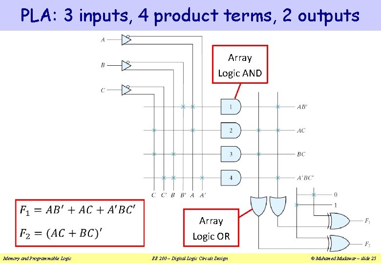
PLA: 3 inputs, 4 product terms, 2 outputs Array Logic AND v Memory and Programmable Logic Array Logic OR EE 200 – Digital Logic Circuit Design © Muhamed Mudawar – slide 25
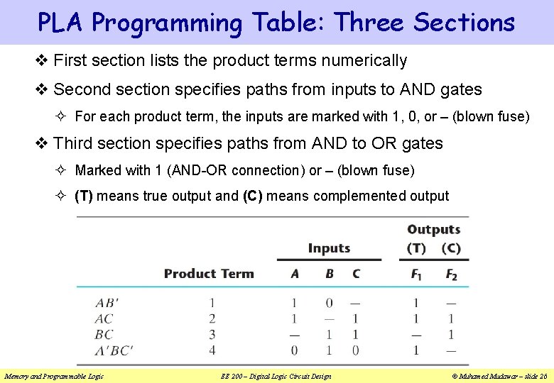
PLA Programming Table: Three Sections v First section lists the product terms numerically v Second section specifies paths from inputs to AND gates ² For each product term, the inputs are marked with 1, 0, or – (blown fuse) v Third section specifies paths from AND to OR gates ² Marked with 1 (AND-OR connection) or – (blown fuse) ² (T) means true output and (C) means complemented output Memory and Programmable Logic EE 200 – Digital Logic Circuit Design © Muhamed Mudawar – slide 26
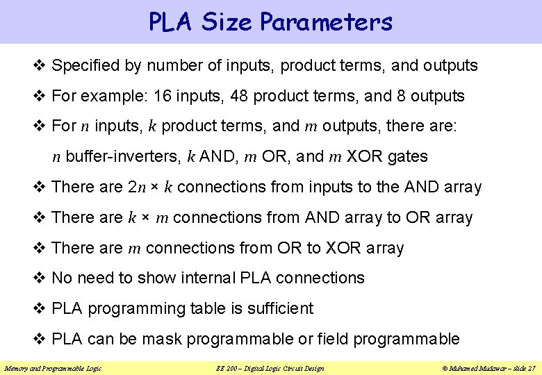
PLA Size Parameters v Specified by number of inputs, product terms, and outputs v For example: 16 inputs, 48 product terms, and 8 outputs v For n inputs, k product terms, and m outputs, there are: n buffer-inverters, k AND, m OR, and m XOR gates v There are 2 n × k connections from inputs to the AND array v There are k × m connections from AND array to OR array v There are m connections from OR to XOR array v No need to show internal PLA connections v PLA programming table is sufficient v PLA can be mask programmable or field programmable Memory and Programmable Logic EE 200 – Digital Logic Circuit Design © Muhamed Mudawar – slide 27
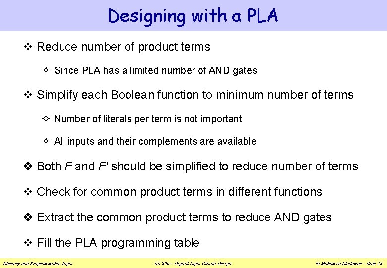
Designing with a PLA v Reduce number of product terms ² Since PLA has a limited number of AND gates v Simplify each Boolean function to minimum number of terms ² Number of literals per term is not important ² All inputs and their complements are available v Both F and F' should be simplified to reduce number of terms v Check for common product terms in different functions v Extract the common product terms to reduce AND gates v Fill the PLA programming table Memory and Programmable Logic EE 200 – Digital Logic Circuit Design © Muhamed Mudawar – slide 28
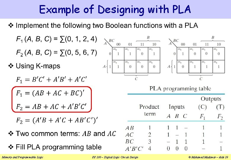
Example of Designing with PLA v Memory and Programmable Logic EE 200 – Digital Logic Circuit Design © Muhamed Mudawar – slide 29
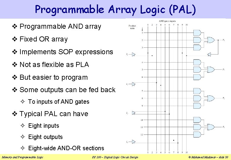
Programmable Array Logic (PAL) v Programmable AND array v Fixed OR array v Implements SOP expressions v Not as flexible as PLA v But easier to program v Some outputs can be fed back ² To inputs of AND gates v Typical PAL can have ² Eight inputs ² Eight outputs ² Eight-wide AND-OR sections Memory and Programmable Logic EE 200 – Digital Logic Circuit Design © Muhamed Mudawar – slide 30
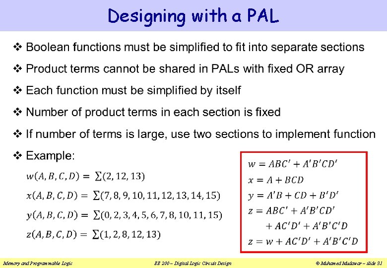
Designing with a PAL v Memory and Programmable Logic EE 200 – Digital Logic Circuit Design © Muhamed Mudawar – slide 31
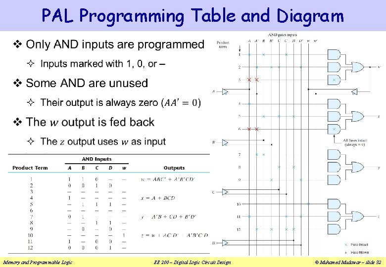
PAL Programming Table and Diagram v Memory and Programmable Logic EE 200 – Digital Logic Circuit Design © Muhamed Mudawar – slide 32
- Slides: 32