
MC 542 Organizao de Computadores Teoria e Prtica

- Slides: 53
MC 542 Organização de Computadores Teoria e Prática 2006 Prof. Paulo Cesar Centoducatte@ic. unicamp. br www. ic. unicamp. br/~ducatte MC 542 1 S 2006 2. 1
MC 542 Circuitos Lógicos Tecnologia de Implementação “Fundamentals of Digital Logic with VHDL Design” - (Capítulo 3) MC 542 1 S 2006 2. 2
Tecnologia de Implementação Sumário • • • Introdução Transistor Como Chave Portas Lógicas NMOS Portas Lógicas CMOS • • • Chips Padrões Gate Array e FPGAs CMOS: Fabricação e Comportamento – MC 542 Lógica Positiva e Negativa 1 S 2006 2. 3
Introdução Valores Lógicos como Voltagem MC 542 1 S 2006 2. 4
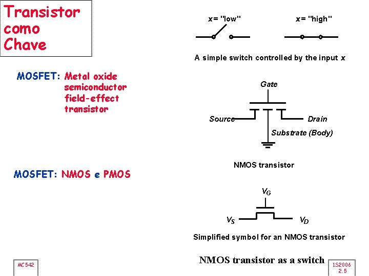
Transistor como Chave MOSFET: Metal oxide semiconductor field-effect transistor x = "low" x = "high" A simple switch controlled by the input x Gate Source Drain Substrate (Body) MOSFET: NMOS e PMOS NMOS transistor VG VS VD Simplified symbol for an NMOS transistor MC 542 NMOS transistor as a switch 1 S 2006 2. 5
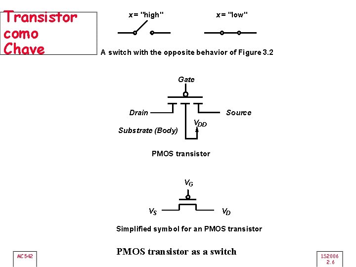
Transistor como Chave x = "high" x = "low" A switch with the opposite behavior of Figure 3. 2 Gate Drain Source VDD Substrate (Body) PMOS transistor VG VS VD Simplified symbol for an PMOS transistor MC 542 PMOS transistor as a switch 1 S 2006 2. 6
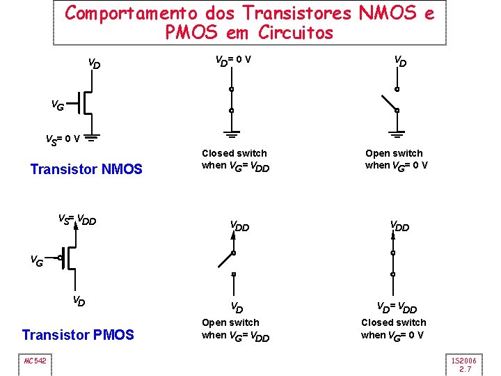
Comportamento dos Transistores NMOS e PMOS em Circuitos VD VD = 0 V VD VG VS= 0 V Transistor NMOS VS= VDD Closed switch when VG = VDD Open switch when VG = 0 V VDD VG VD Transistor PMOS MC 542 VD Open switch when VG = VDD VD = VDD Closed switch when VG = 0 V 1 S 2006 2. 7
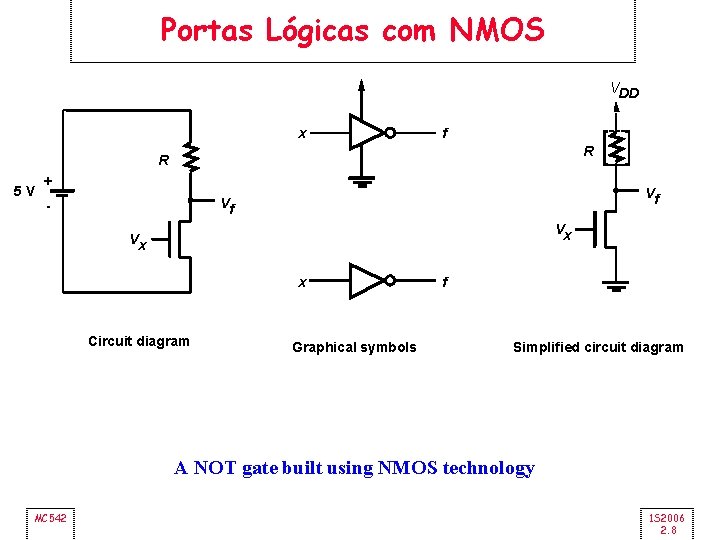
Portas Lógicas com NMOS VDD x f R R 5 V + Vf Vf - Vx Vx x Circuit diagram Graphical symbols f Simplified circuit diagram A NOT gate built using NMOS technology MC 542 1 S 2006 2. 8
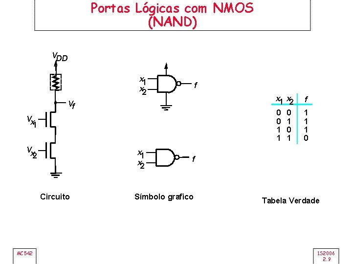
Portas Lógicas com NMOS (NAND) VDD x 1 x 2 f x 1 0 0 1 1 Vf Vx 1 Vx 2 x 1 x 2 Circuito MC 542 x 2 0 1 f 1 1 1 0 f Símbolo grafico Tabela Verdade 1 S 2006 2. 9
Portas Lógicas com NMOS (NOR) MC 542 1 S 2006 2. 10
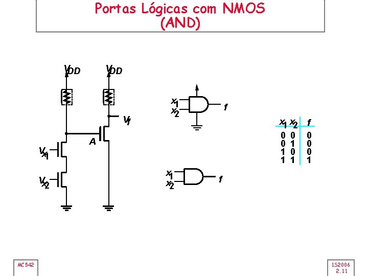
Portas Lógicas com NMOS (AND) VDD Vf Vx 1 Vx 2 MC 542 x 1 x 2 f x 1 x 2 0 0 0 1 1 A x 1 x 2 f 0 0 0 1 f 1 S 2006 2. 11
Portas Lógicas com NMOS (OR) MC 542 1 S 2006 2. 12
Estrutura de um circuito NMOS MC 542 1 S 2006 2. 13
Estrutura de um Circuito CMOS (NMOS + PMOS) A função é implementada por uma rede Nmos e uma Pmos simultaneamente MC 542 1 S 2006 2. 14
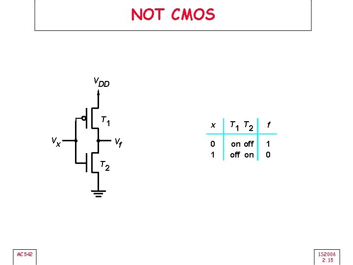
NOT CMOS VDD T 1 Vx Vf T MC 542 x T 2 f 0 1 on off on 1 0 1 T 2 1 S 2006 2. 15
NAND CMOS f = x 1 + x 2 PUN PDN f = x 1. x 2 MC 542 1 S 2006 2. 16
NOR CMOS f = x 1. x 2 PUN PDN f = x 1+x 2 MC 542 1 S 2006 2. 17
AND CMOS MC 542 1 S 2006 2. 18
Exemplo: Circuito Complexo f = x 1 + x 2 x 3 MC 542 1 S 2006 2. 19
Exercício Qual a função implementada por: f = x 1 (x 2 x 3 + x 4) MC 542 1 S 2006 2. 20
Níveis de Tensão no Circuito Tensão no circuito MC 542 1 S 2006 2. 21
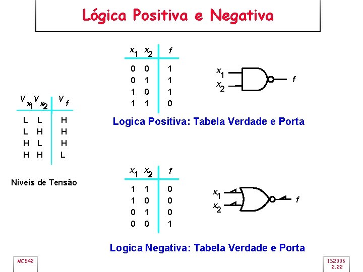
Lógica Positiva e Negativa V V x 1 x 2 L L H H L H V f H H H L Níveis de Tensão x x 1 2 f 0 0 1 1 1 0 0 1 x 1 x 2 f Logica Positiva: Tabela Verdade e Porta x x 1 2 f 1 1 0 0 0 1 1 0 x 1 x 2 f Logica Negativa: Tabela Verdade e Porta MC 542 1 S 2006 2. 22
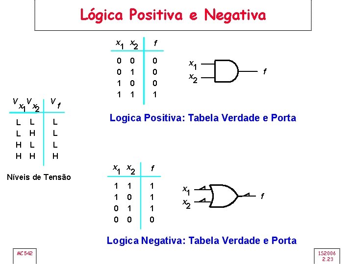
Lógica Positiva e Negativa V V x 1 x 2 L L H H L H V x x 1 2 f 0 0 1 1 0 0 0 1 0 1 x 2 f f L L L H Níveis de Tensão Logica Positiva: Tabela Verdade e Porta x x 1 2 f 1 1 0 0 1 1 1 0 1 0 x 1 x 2 f Logica Negativa: Tabela Verdade e Porta MC 542 1 S 2006 2. 23
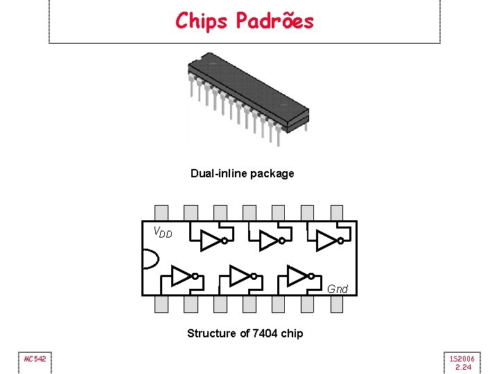
Chips Padrões Dual-inline package VDD Gnd Structure of 7404 chip MC 542 1 S 2006 2. 24
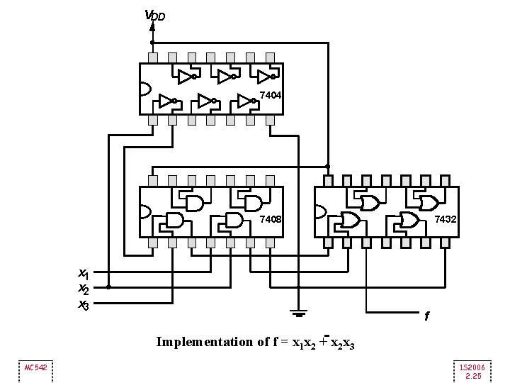
VDD 7404 7408 x 1 x 2 x 3 7432 f Implementation of f = x 1 x 2 + x 2 x 3 MC 542 1 S 2006 2. 25
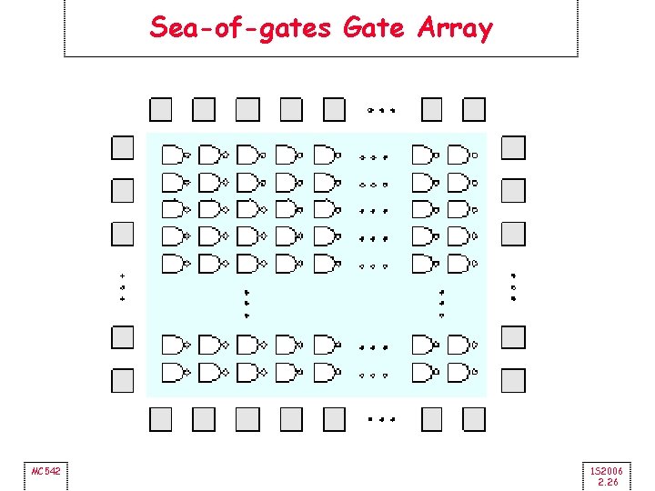
Sea-of-gates Gate Array MC 542 1 S 2006 2. 26
Gate Array MC 542 1 S 2006 2. 27
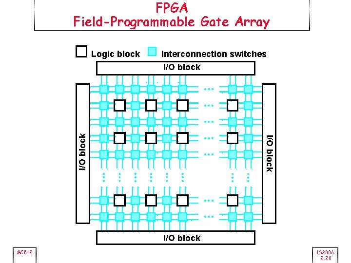
FPGA Field-Programmable Gate Array Interconnection switches I/O block Logic block I/O block MC 542 1 S 2006 2. 28
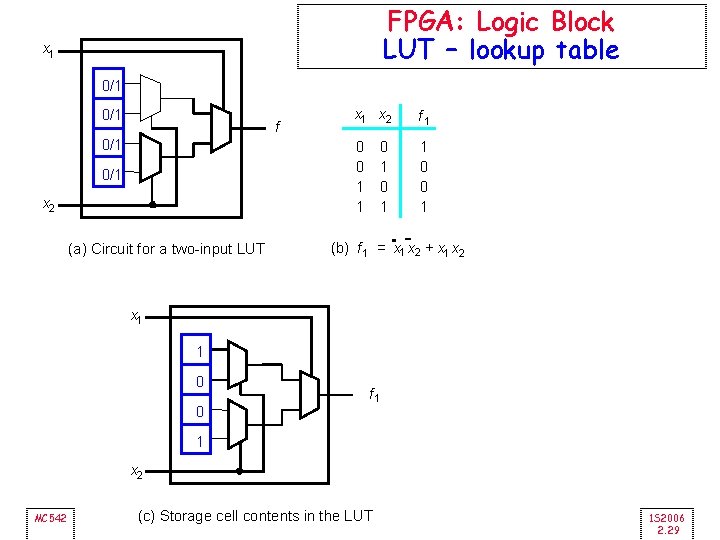
FPGA: Logic Block LUT – lookup table x 1 0/1 f 0/1 x 2 (a) Circuit for a two-input LUT x 1 x 2 f 1 0 0 1 1 1 0 0 1 0 1 (b) f 1 = x 1 x 2 + x 1 x 2 x 1 1 0 0 f 1 1 x 2 MC 542 (c) Storage cell contents in the LUT 1 S 2006 2. 29
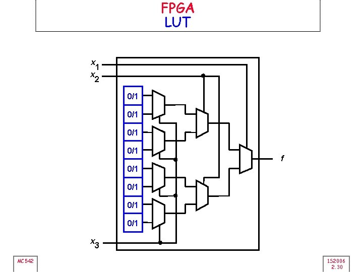
FPGA LUT x x 1 2 0/1 0/1 f 0/1 0/1 x MC 542 3 1 S 2006 2. 30
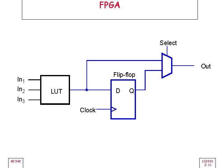
FPGA Select Out Flip-flop In 1 In 2 D LUT Q In 3 Clock MC 542 1 S 2006 2. 31
FPGA MC 542 1 S 2006 2. 32
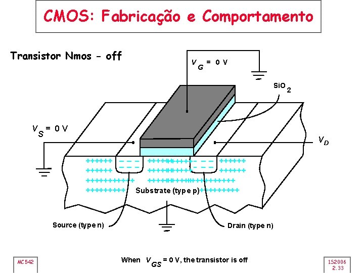
CMOS: Fabricação e Comportamento Transistor Nmos - off V G = 0 V Si. O V S 2 = 0 V VD ++++++ ++++++ ++++++ +++++++++++ Substrate (type p)+++++ Source (type n) MC 542 Drain (type n) When V GS = 0 V, the transistor is off 1 S 2006 2. 33
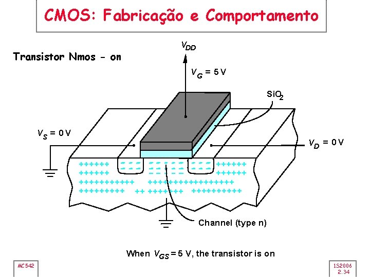
CMOS: Fabricação e Comportamento Transistor Nmos - on VDD VG = 5 V Si. O 2 VS = 0 V VD = 0 V ++++++ ++++++++++++ ++ ++++++++++ Channel (type n) When VGS = 5 V, the transistor is on MC 542 1 S 2006 2. 34
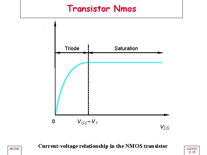
Transistor Nmos I D Triode 0 MC 542 V GS – V T Saturation VDS Current-voltage relationship in the NMOS transistor 1 S 2006 2. 35
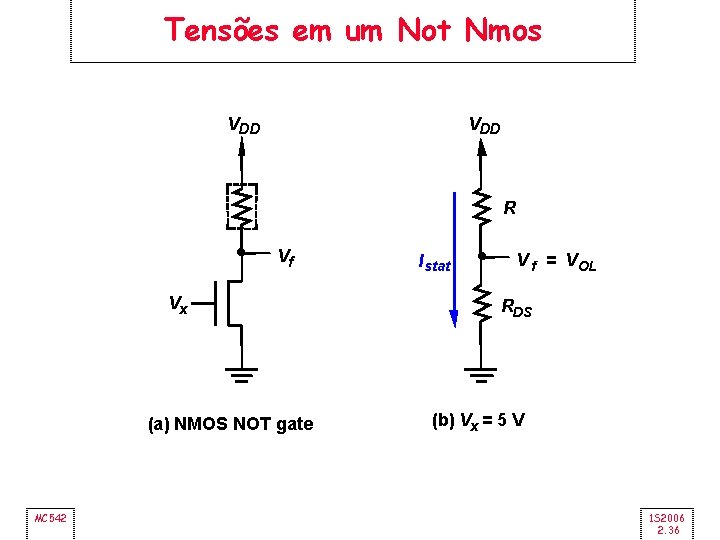
Tensões em um Not Nmos VDD R Vf Vx (a) NMOS NOT gate MC 542 I stat V f = V OL RDS (b) Vx = 5 V 1 S 2006 2. 36
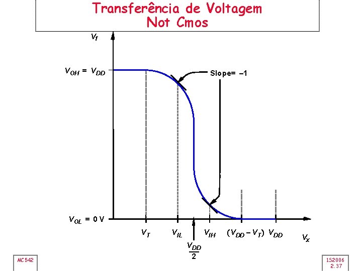
Transferência de Voltagem Not Cmos Vf V OH = V DD Slope = – 1 V OL = 0 V VT MC 542 V IL V IH V DD — 2 ( V DD – V T ) V DD Vx 1 S 2006 2. 37
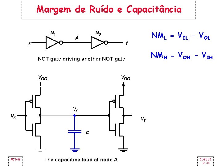
Margem de Ruído e Capacitância N 1 x NML = VIL - VOL N 2 A f NMH = VOH - VIH NOT gate driving another NOT gate VDD VA Vx Vf C MC 542 The capacitive load at node A 1 S 2006 2. 38
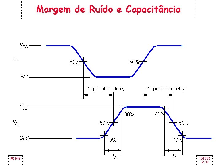
Margem de Ruído e Capacitância VDD Vx 50% Gnd Propagation delay VDD 90% VA 90% 50% Gnd MC 542 10% tr 10% tf 1 S 2006 2. 39
Transistor MOS MC 542 1 S 2006 2. 40
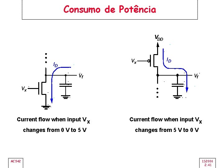
Consumo de Potência VDD Vx ID Vf Vx Current flow when input Vx changes from 0 V to 5 V changes from 5 V to 0 V MC 542 1 S 2006 2. 41
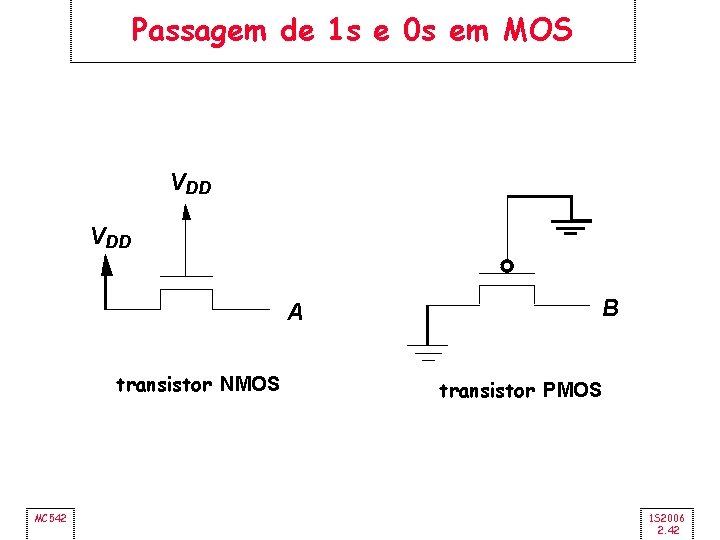
Passagem de 1 s e 0 s em MOS VDD B A transistor NMOS MC 542 transistor PMOS 1 S 2006 2. 42
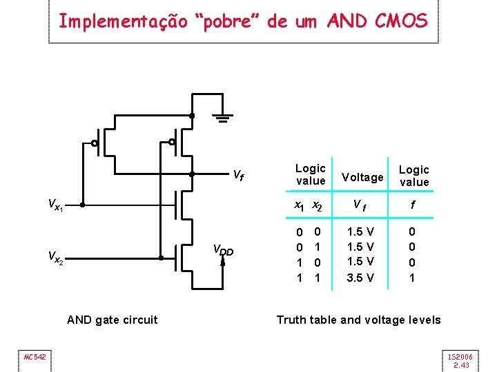
Implementação “pobre” de um AND CMOS Vf Vx 1 x 2 Vx 2 0 0 1 1 VDD AND gate circuit MC 542 Logic value 0 1 Voltage Logic value Vf f 1. 5 V 3. 5 V 0 0 0 1 Truth table and voltage levels 1 S 2006 2. 43
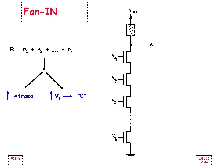
Fan-IN V DD V f R = r 1 + r 2 + …. + rk V x 1 V x 2 Atraso Vf “ 0” V x 3 V xk MC 542 1 S 2006 2. 44
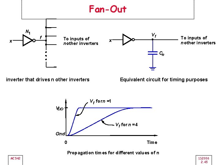
Fan-Out N 1 x f To inputs of n other inverters Vf x To inputs of n other inverters Cn inverter that drives n other inverters Equivalent circuit for timing purposes V f forn =1 VDD V f for n = 4 Gnd 0 Time Propagation times for different values of n MC 542 1 S 2006 2. 45
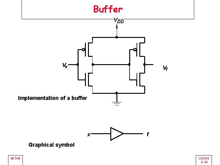
Buffer VDD Vx Vf Implementation of a buffer x f Graphical symbol MC 542 1 S 2006 2. 46
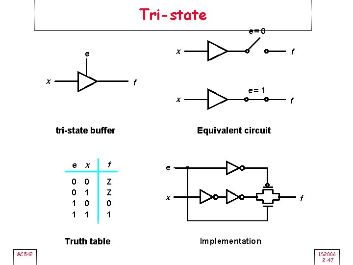
Tri-state e= 0 x e x f x tri-state buffer f e 0 0 1 1 Z Z 0 1 x Truth table MC 542 e= 1 f Equivalent circuit e x 0 1 f f Implementation 1 S 2006 2. 47
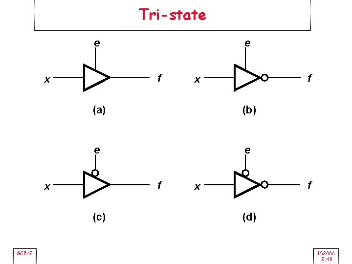
Tri-state e f x (a) (b) e e f x (c) MC 542 e f x (d) 1 S 2006 2. 48
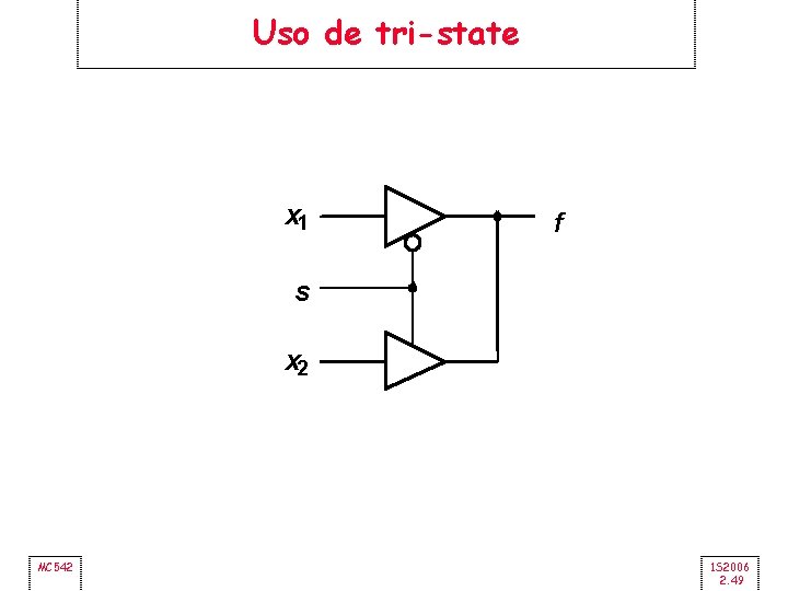
Uso de tri-state x 1 f s x 2 MC 542 1 S 2006 2. 49
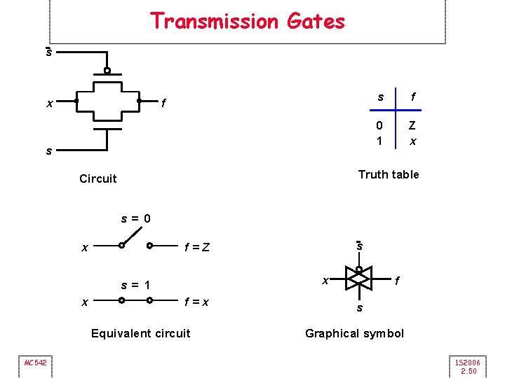
Transmission Gates s x f s s f 0 1 Z x Truth table Circuit s= 0 x x s= 1 x f=x Equivalent circuit MC 542 s f=Z f s Graphical symbol 1 S 2006 2. 50
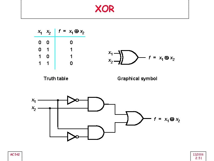
XOR x 1 x 2 0 0 1 1 f = x 1 Å x 2 0 1 Truth table 0 1 1 0 x 1 x 2 f = x 1 Å x 2 Graphical symbol x 1 x 2 f = x 1 Å x 2 MC 542 1 S 2006 2. 51
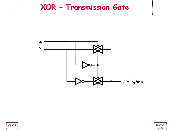
XOR – Transmission Gate x 1 x 2 f = x 1 Å x 2 MC 542 1 S 2006 2. 52
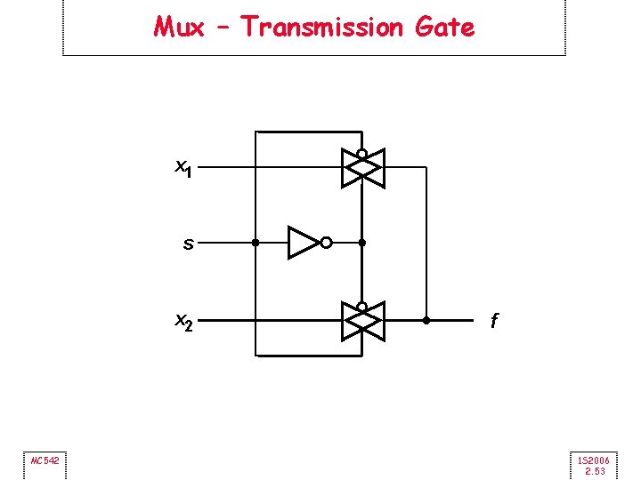
Mux – Transmission Gate x 1 s x 2 MC 542 f 1 S 2006 2. 53