Massachusetts Institute of Technology Laboratory for Electromagnetic and
Massachusetts Institute of Technology Laboratory for Electromagnetic and Electronic Systems Group Meeting July 21, 2009 Justin Burkhart
Presentation Outline n More Exact Analysis of Class E Resonant Boost Converter n Gate Drive Options n Transistor Layout Optimization
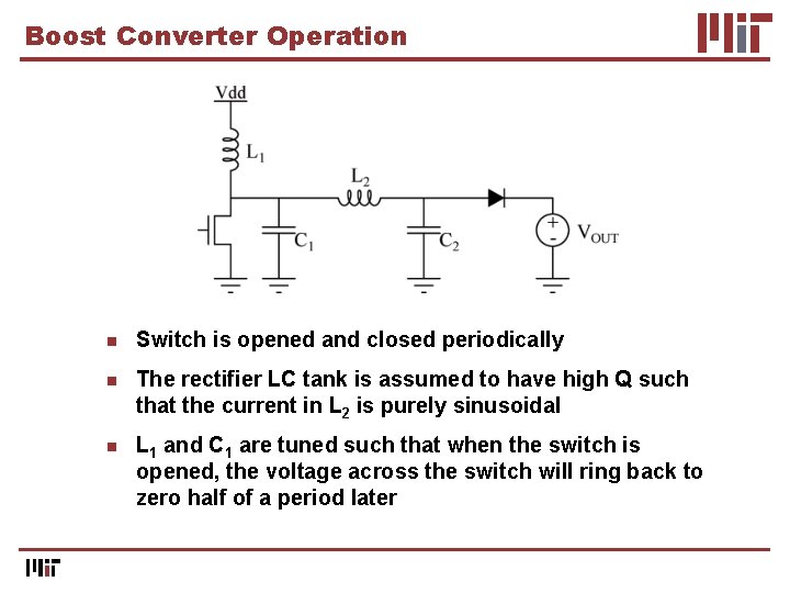
Boost Converter Operation n Switch is opened and closed periodically n The rectifier LC tank is assumed to have high Q such that the current in L 2 is purely sinusoidal n L 1 and C 1 are tuned such that when the switch is opened, the voltage across the switch will ring back to zero half of a period later
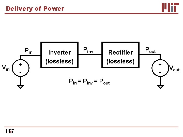
Delivery of Power Pin Vin + - Inverter (lossless) Pinv Rectifier (lossless) Pin = Pinv = Pout + - Vout
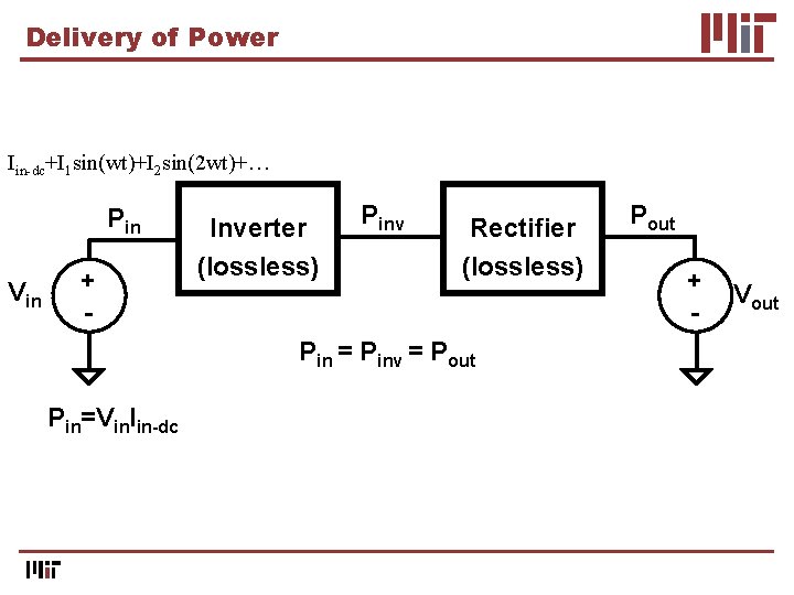
Delivery of Power Iin-dc+I 1 sin(wt)+I 2 sin(2 wt)+… Pin Vin + - Inverter (lossless) Pinv Rectifier (lossless) Pin = Pinv = Pout Pin=Vin. Iin-dc Pout + - Vout
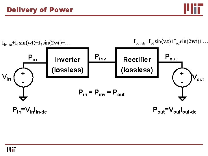
Delivery of Power Iout-dc+Io 1 sin(wt)+Io 2 sin(2 wt)+… Iin-dc+I 1 sin(wt)+I 2 sin(2 wt)+… Pin Vin + - Inverter (lossless) Pinv Rectifier (lossless) Pout + - Vout Pin = Pinv = Pout Pin=Vin. Iin-dc Pout=Vout. Iout-dc
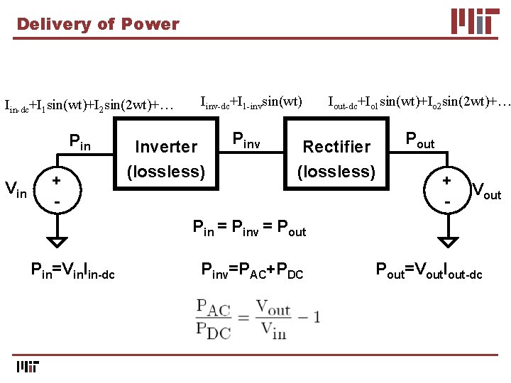
Delivery of Power Iin-dc+I 1 sin(wt)+I 2 sin(2 wt)+… Pin Vin + - Iinv-dc+I 1 -invsin(wt) Inverter (lossless) Pinv Iout-dc+Io 1 sin(wt)+Io 2 sin(2 wt)+… Rectifier (lossless) Pout + - Vout Pin = Pinv = Pout Pin=Vin. Iin-dc Pinv=PAC+PDC Pout=Vout. Iout-dc
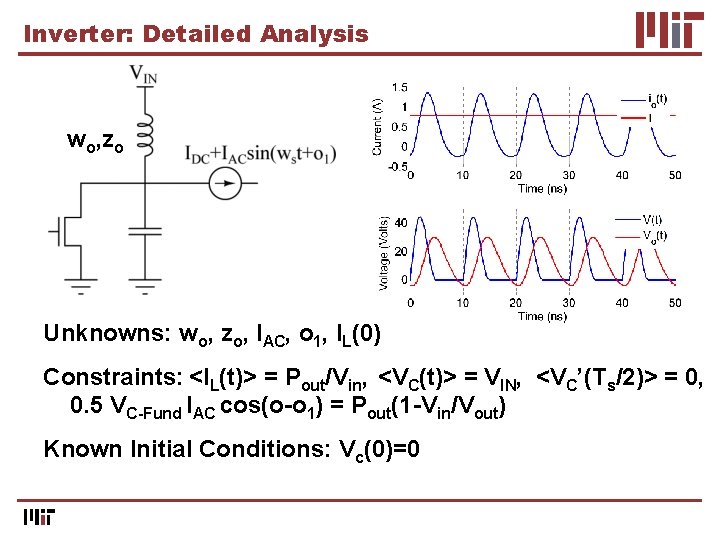
Inverter: Detailed Analysis wo, zo Unknowns: wo, zo, IAC, o 1, IL(0) Constraints: <IL(t)> = Pout/Vin, <VC(t)> = VIN, <VC’(Ts/2)> = 0, 0. 5 VC-Fund IAC cos(o-o 1) = Pout(1 -Vin/Vout) Known Initial Conditions: Vc(0)=0
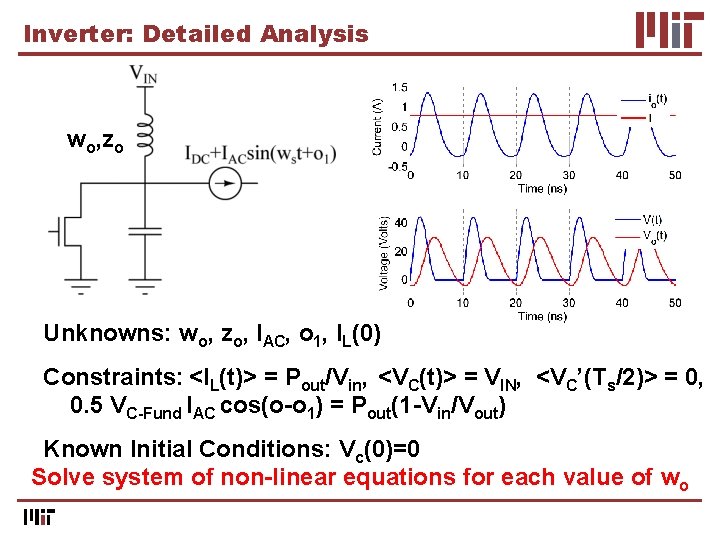
Inverter: Detailed Analysis wo, zo Unknowns: wo, zo, IAC, o 1, IL(0) Constraints: <IL(t)> = Pout/Vin, <VC(t)> = VIN, <VC’(Ts/2)> = 0, 0. 5 VC-Fund IAC cos(o-o 1) = Pout(1 -Vin/Vout) Known Initial Conditions: Vc(0)=0 Solve system of non-linear equations for each value of wo
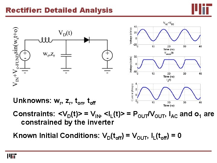
Rectifier: Detailed Analysis Unknowns: wr, zr, ton, toff Constraints: <VD(t)> = VIN, <IL(t)> = POUT/VOUT, IAC and o 1 are constrained by the inverter Known Initial Conditions: VD(toff) = VOUT, IL(toff) = 0
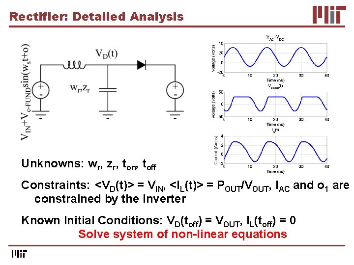
Rectifier: Detailed Analysis Unknowns: wr, zr, ton, toff Constraints: <VD(t)> = VIN, <IL(t)> = POUT/VOUT, IAC and o 1 are constrained by the inverter Known Initial Conditions: VD(toff) = VOUT, IL(toff) = 0 Solve system of non-linear equations
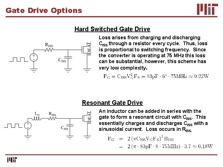
Gate Drive Options Hard Switched Gate Drive Loss arises from charging and discharging CISS through a resistor every cycle. Thus, loss is proportional to switching frequency. Since the converter is operating at 75 MHz this loss can be substantial, however, this scheme has very low complexity. Resonant Gate Drive An inductor can be added in series with the gate to form a resonant circuit with CISS. This essentially charges and discharges CISS with a sinusoidal current. Loss occurs in RISS.
Introduction to TI’s LBC 5 Process Removed

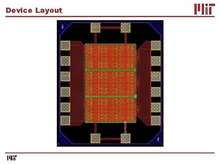
LDMOS Layout Removed
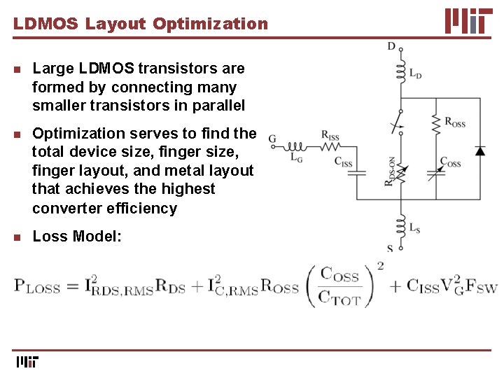
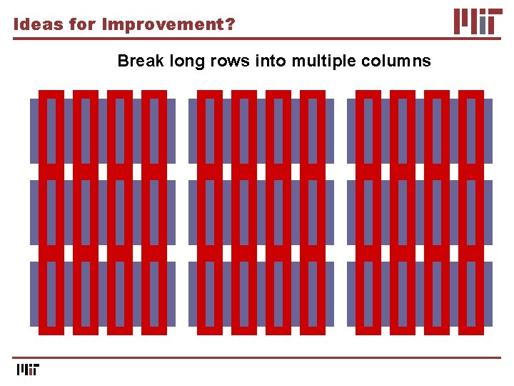
LDMOS Layout Optimization n Large LDMOS transistors are formed by connecting many smaller transistors in parallel n Optimization serves to find the total device size, finger layout, and metal layout that achieves the highest converter efficiency n Loss Model:
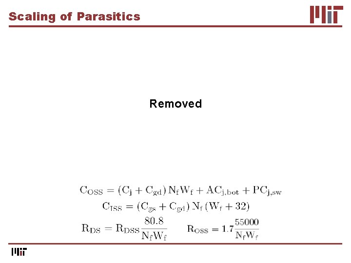
Scaling of Parasitics Removed
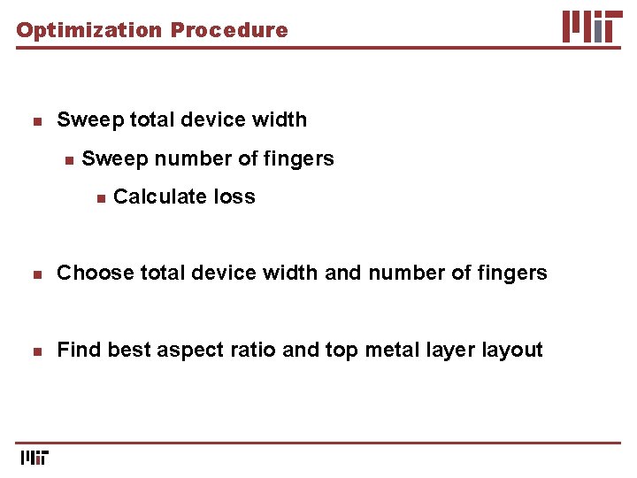
Optimization Procedure n Sweep total device width n Sweep number of fingers n Calculate loss n Choose total device width and number of fingers n Find best aspect ratio and top metal layer layout
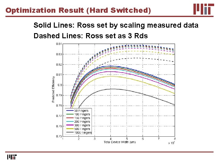
Optimization Result (Hard Switched) Solid Lines: Ross set by scaling measured data Dashed Lines: Ross set as 3 Rds
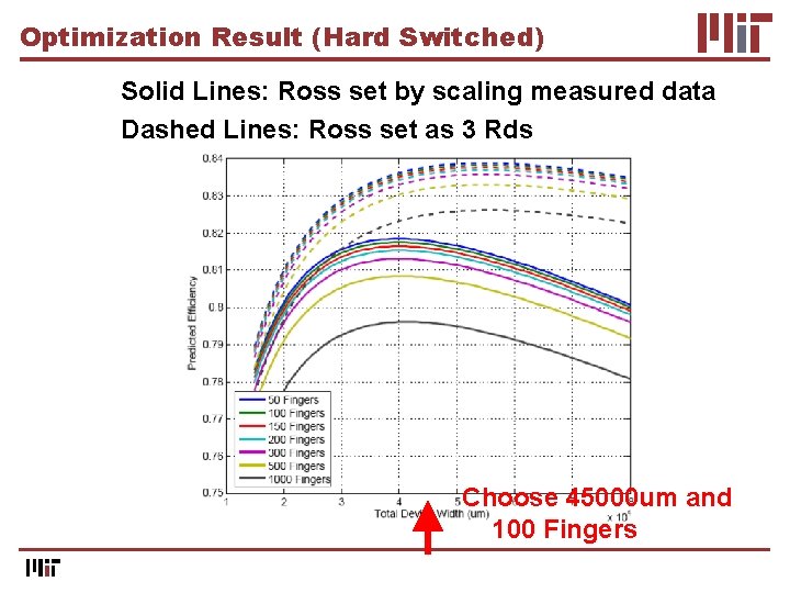
Optimization Result (Hard Switched) Solid Lines: Ross set by scaling measured data Dashed Lines: Ross set as 3 Rds Choose 45000 um and 100 Fingers
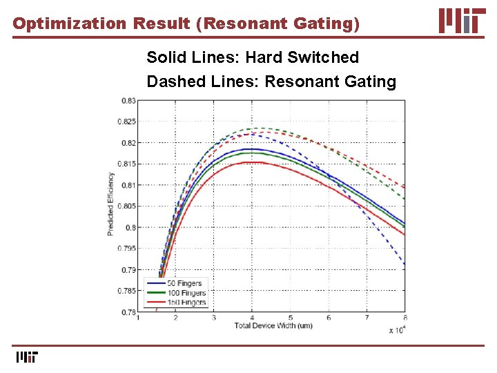
Optimization Result (Resonant Gating) Solid Lines: Hard Switched Dashed Lines: Resonant Gating
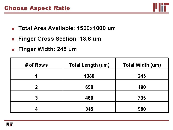
Choose Aspect Ratio n Total Area Available: 1500 x 1000 um n Finger Cross Section: 13. 8 um n Finger Width: 245 um # of Rows Total Length (um) Total Width (um) 1 1380 245 2 690 490 3 460 735 4 345 980
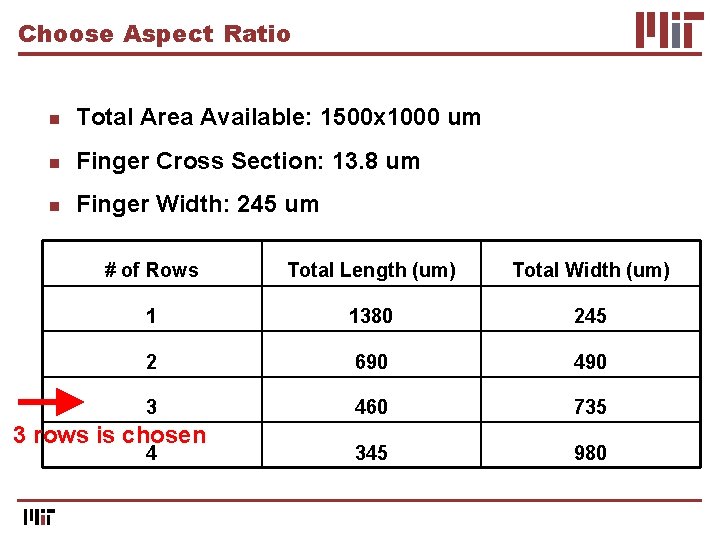
Choose Aspect Ratio n Total Area Available: 1500 x 1000 um n Finger Cross Section: 13. 8 um n Finger Width: 245 um # of Rows Total Length (um) Total Width (um) 1 1380 245 2 690 490 3 460 735 345 980 3 rows is chosen 4
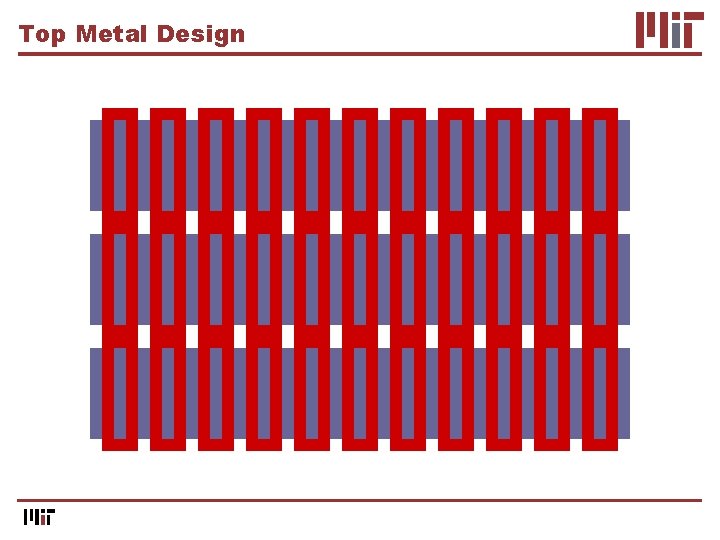
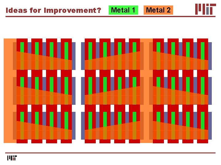
Top Metal Design
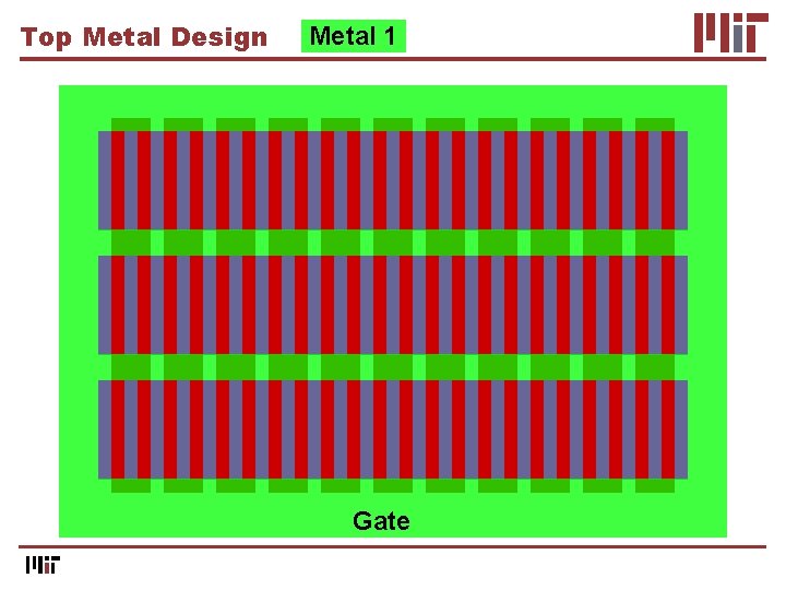
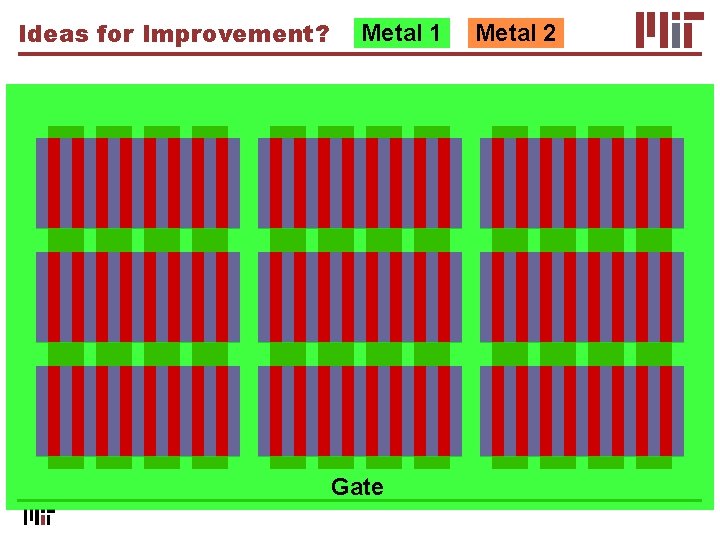
Top Metal Design Metal 1 Gate
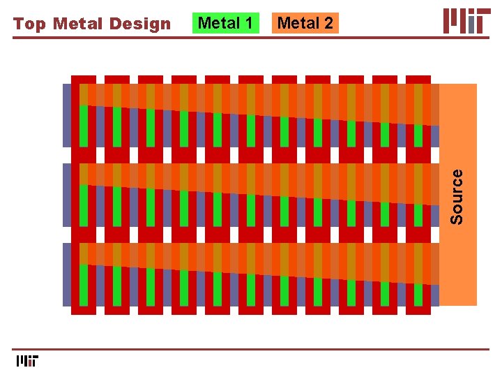
Metal 1 Metal 2 Source Top Metal Design
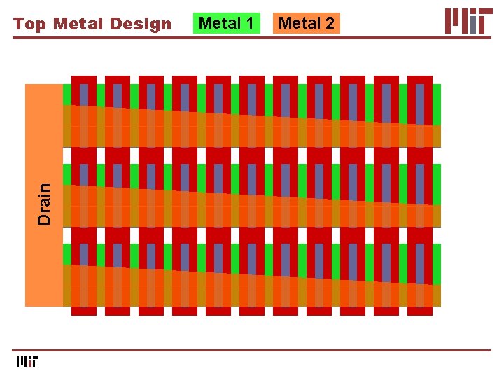
Drain Top Metal Design Metal 1 Metal 2
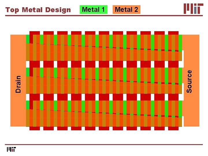
Metal 1 Metal 2 Source Drain Top Metal Design
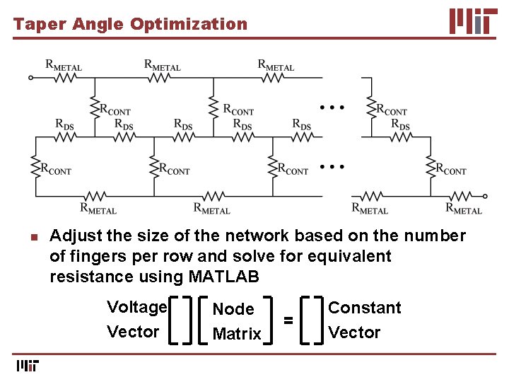
Taper Angle Optimization n Adjust the size of the network based on the number of fingers per row and solve for equivalent resistance using MATLAB Voltage Vector Node Matrix Constant Vector
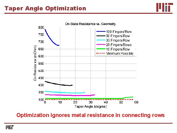
Taper Angle Optimization ignores metal resistance in connecting rows
Device Layout
Ideas for Improvement? Break long rows into multiple columns
Ideas for Improvement? Metal 1 Gate Metal 2
Ideas for Improvement? Metal 1 Metal 2
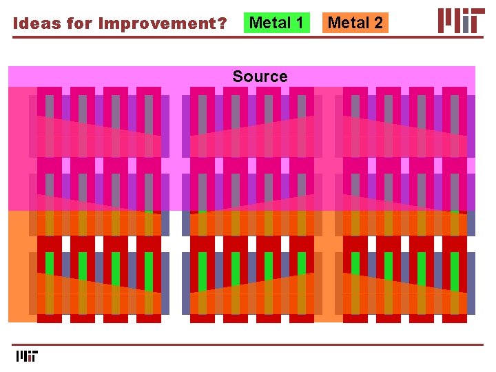
Ideas for Improvement? Metal 1 Source Metal 2
- Slides: 34