Mask Design Training Quality Layout Page 1 Mask


- Slides: 30

Mask Design Training Quality Layout Page 1

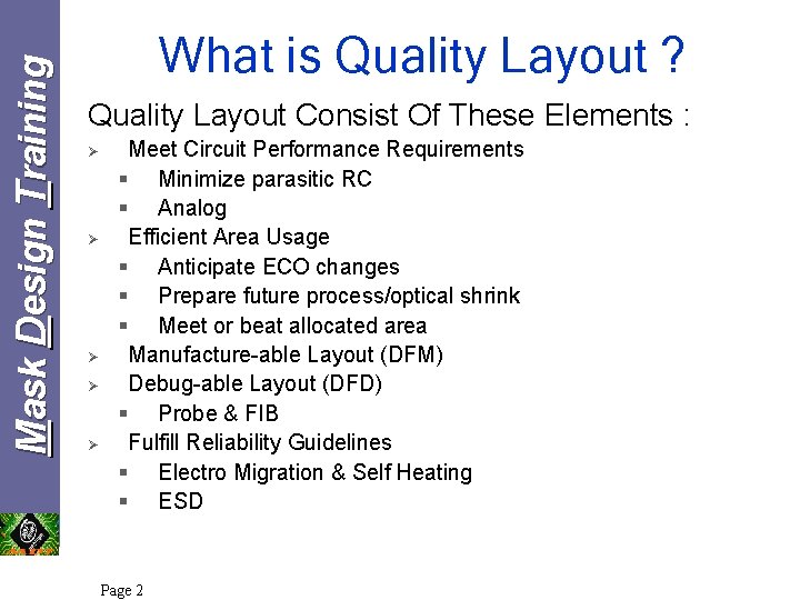
Mask Design Training What is Quality Layout ? Quality Layout Consist Of These Elements : Ø Ø Ø Meet Circuit Performance Requirements § Minimize parasitic RC § Analog Efficient Area Usage § Anticipate ECO changes § Prepare future process/optical shrink § Meet or beat allocated area Manufacture-able Layout (DFM) Debug-able Layout (DFD) § Probe & FIB Fulfill Reliability Guidelines § Electro Migration & Self Heating § ESD Page 2

Mask Design Training OUTLINES Ø Engineering Layout Checklist ü ü ü Ø Ø Poly Guidelines Contact Guidelines Diffussion Guidelines Metal and Vias Guidelines Summary Electromigration and Self Heating Layout Review Checklist Page 3

Mask Design Training Poly Guidelines Polysilicons In general, poly has much higher resistance then metal and therefore much higher delay. Using poly as an interconnect level can be advantageously used to create very compacts layout. But, poly should never be used as interconnect when the capacitance is high. Page 4

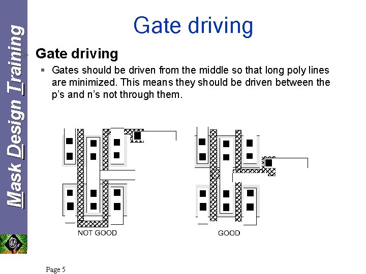
Mask Design Training Ø Gate driving § Gates should be driven from the middle so that long poly lines are minimized. This means they should be driven between the p’s and n’s not through them. Page 5

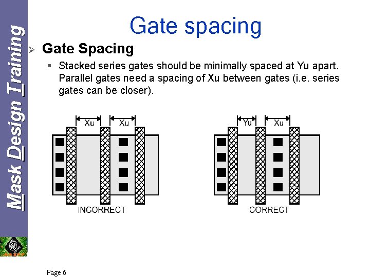
Mask Design Training Gate spacing Ø Gate Spacing § Stacked series gates should be minimally spaced at Yu apart. Parallel gates need a spacing of Xu between gates (i. e. series gates can be closer). Page 6

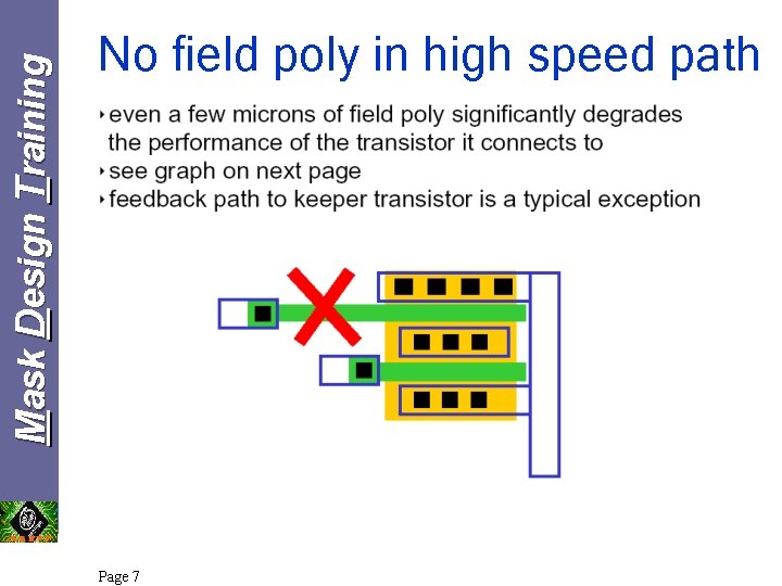
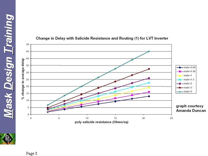
Mask Design Training No field poly in high speed path Page 7

Page 8 Mask Design Training

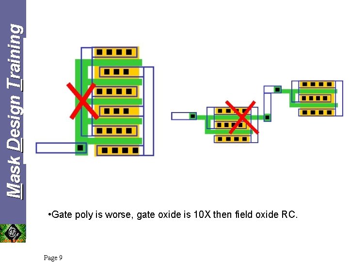
Mask Design Training • Gate poly is worse, gate oxide is 10 X then field oxide RC. Page 9

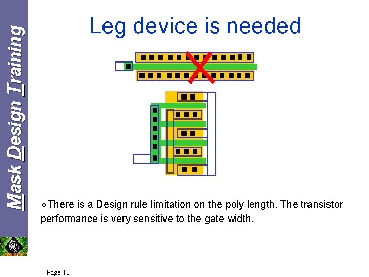
Mask Design Training Leg device is needed v. There is a Design rule limitation on the poly length. The transistor performance is very sensitive to the gate width. Page 10

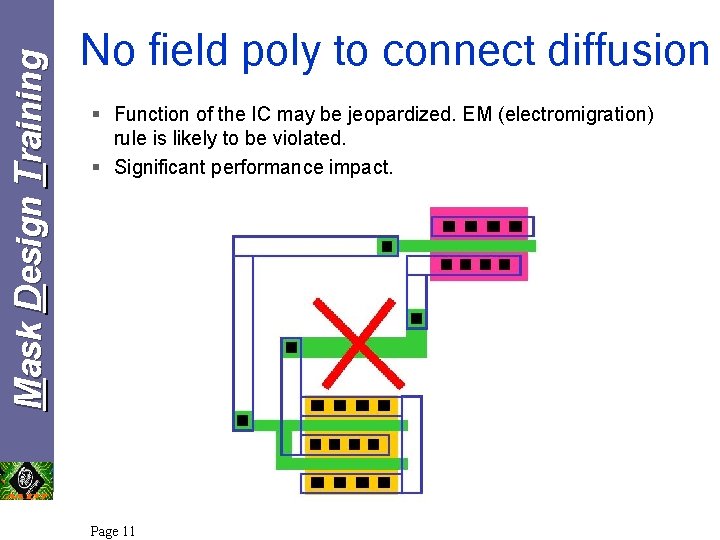
Mask Design Training No field poly to connect diffusion § Function of the IC may be jeopardized. EM (electromigration) rule is likely to be violated. § Significant performance impact. Page 11

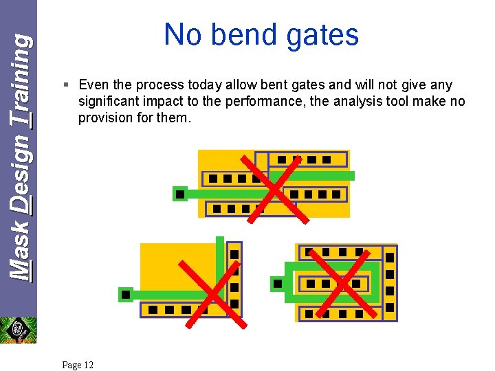
Mask Design Training No bend gates § Even the process today allow bent gates and will not give any significant impact to the performance, the analysis tool make no provision for them. Page 12

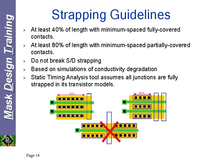
Mask Design Training Contacts Guidelines Ø There are two kinds of contacts: partially covered and fully covered. Partially covered contacts cannot carry as much current as fully covered contacts. Definitions Fully/Partially Covered: A fully covered contacts has at least 0. 16 u coverage on all sides. A partially covered contact has 0. 0 metal coverage past the edge of the contact. This mean that during process, if the mask moves, the partially covered contact may not be covered all the way with metal. Ø Fully/Partially Strapped: Strapping is a term indicating how many contacts connect the device to metal 1. Fully strapped means that as many contact as will fit have been placed on the device. Partially strapped means that some of the contacts is missing. Page 13

Mask Design Training Strapping Guidelines Ø Ø Ø At least 40% of length with minimum-spaced fully-covered contacts. At least 80% of length with minimum-spaced partially-covered contacts. Do not break S/D strapping Based on simulations of conductivity degradation Static Timing Analysis tool assumes all junctions are fully strapped in its transistor models. Page 14

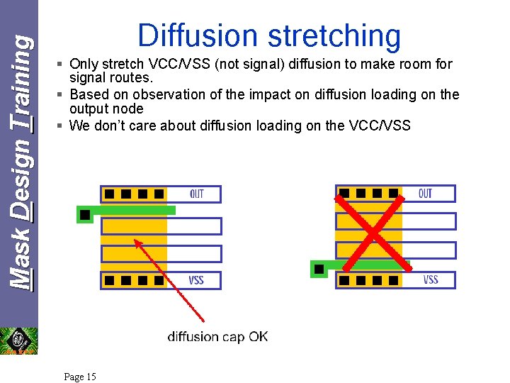
Mask Design Training Diffusion stretching § Only stretch VCC/VSS (not signal) diffusion to make room for signal routes. § Based on observation of the impact on diffusion loading on the output node § We don’t care about diffusion loading on the VCC/VSS Page 15

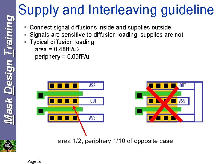
Mask Design Training Supply and Interleaving guideline § Connect signal diffusions inside and supplies outside § Signals are sensitive to diffusion loading, supplies are not § Typical diffusion loading area = 0. 48 f. F/u 2 periphery = 0. 05 f. F/u Page 16

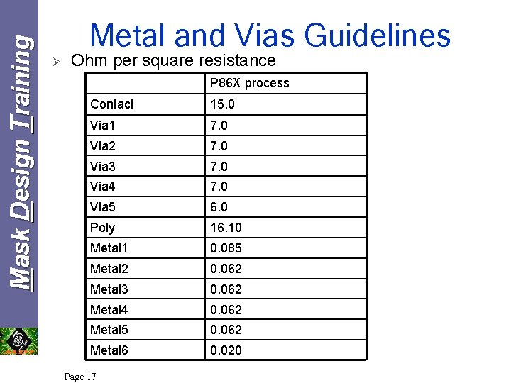
Mask Design Training Metal and Vias Guidelines Ø Ohm per square resistance P 86 X process Contact 15. 0 Via 1 7. 0 Via 2 7. 0 Via 3 7. 0 Via 4 7. 0 Via 5 6. 0 Poly 16. 10 Metal 1 0. 085 Metal 2 0. 062 Metal 3 0. 062 Metal 4 0. 062 Metal 5 0. 062 Metal 6 0. 020 Page 17

Mask Design Training Ø Metals Metal 1 will be unusable for longer routes as refer to the chart of ohm/square. Metal 1 is more resistive compared to others metal layer, therefore move to Metal 2 as soon as possible when do a signal routing to minimize the RC delay. Ø Vias are allowed to be stacked. Via stacking rules: 1. Via 1 may stack on well, diff and poly and directly on top of contact. 2. Via 2 may stack on contact and directly Via 1 without constraint. 3. Via 3 may stack on contact, Via 1 and directly Via 2 without constraint. 4. Via 4 may stack on contact, Via 1, Via 2 and directly Via 3 without constraint. Page 18

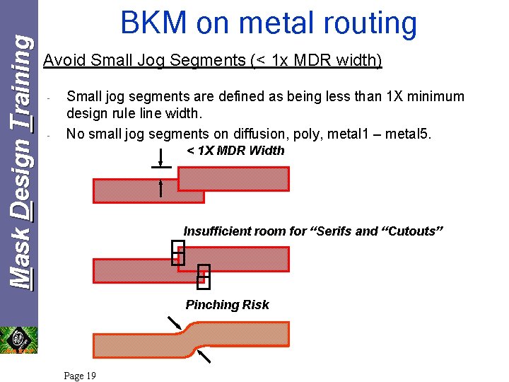
Mask Design Training BKM on metal routing Avoid Small Jog Segments (< 1 x MDR width) - - Small jog segments are defined as being less than 1 X minimum design rule line width. No small jog segments on diffusion, poly, metal 1 – metal 5. < 1 X MDR Width Insufficient room for “Serifs and “Cutouts” Pinching Risk Page 19

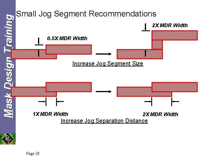
Mask Design Training Small Jog Segment Recommendations 2 X MDR Width 0. 5 X MDR Width Increase Jog Segment Size 1 X MDR Width 2 X MDR Width Increase Jog Separation Distance Page 20

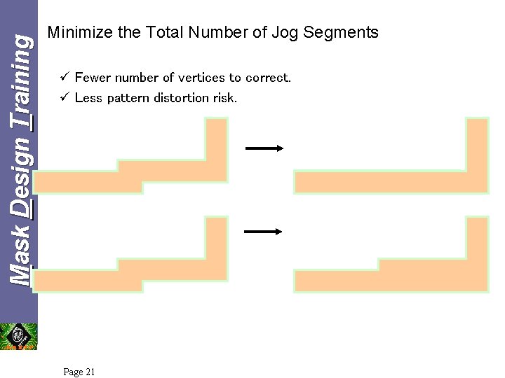
Mask Design Training Minimize the Total Number of Jog Segments ü Fewer number of vertices to correct. ü Less pattern distortion risk. Page 21

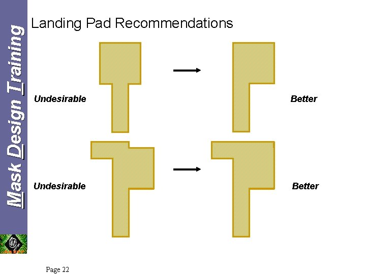
Mask Design Training Landing Pad Recommendations Undesirable Better Page 22

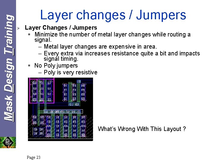
Mask Design Training Layer changes / Jumpers Ø Layer Changes / Jumpers § Minimize the number of metal layer changes while routing a signal. – Metal layer changes are expensive in area. – Every extra via increases resistance quite a bit and impacts signal timing. § No Poly jumpers – Poly is very resistive What’s Wrong With This Layout ? Page 23

Mask Design Training Summary Ø Shareable Power/Ground § Ensure shareable power/ground at diffusion edges if possible. § Always connect to bigger supply (ie: metal 2 with 2 vias width). Ø Well Taps & Substrate Taps § Have well taps connect to VDD or signal specified in schematic. § Have substrate taps connect to GND. Ø Shareable Nodes § Share nodes both internally and externally as much as possible. – Sharing nodes can reduce cell or block size/area. – Sharing nodes can reduce contacts, vias and metal layers used. § Help to improve circuit performance. § Not applicable for special circuit (ie: analog – matching layout). Page 24

Mask Design Training Ø Metal Directions § Use consistent metal directions for M 1, M 2, and M 3. Make sure that tracks are not blocked by using inconsistent directions. M 1 and M 3 vertical, M 2 and M 4 horizontal. Ø Routing Jogs / turning points § Avoid making unnecessary jogs in routing (i. e. if a wire can go straight it should). This will help performance and area. § Aligned the placement of connectors to signal to avoid creating unnecessary curves / corners. Ø Signal Width § Try to maintain uniform/even width for a signal. § Check with DE or layout lead on critical / HV signal width requirement. Page 25

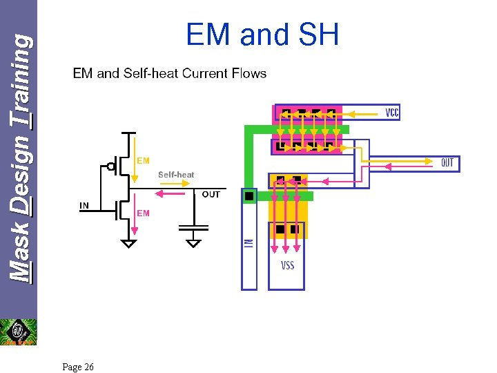
Mask Design Training EM and SH Page 26

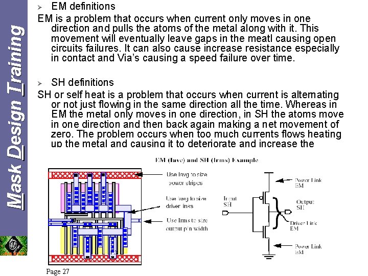
EM definitions EM is a problem that occurs when current only moves in one direction and pulls the atoms of the metal along with it. This movement will eventually leave gaps in the meatl causing open circuits failures. It can also cause increase resistance especially in contact and Via’s causing a speed failure over time. Mask Design Training Ø SH definitions SH or self heat is a problem that occurs when current is alternating or not just flowing in the same direction all the time. Whereas in EM the metal only moves in one direction, in SH the atoms move in one direction and then back again making a net movement of zero. The problem occurs when too much currents flows heating up the metal and causing it to deteriorate and increase the resistance. Ø Page 27

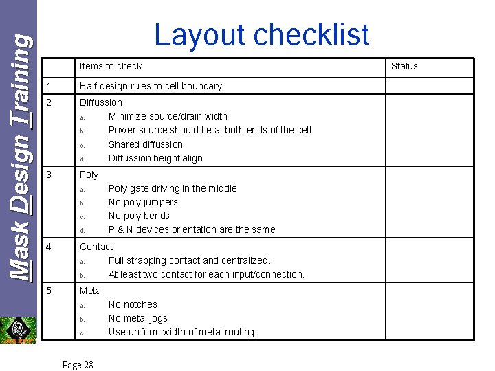
Mask Design Training Layout checklist Items to check 1 Half design rules to cell boundary 2 Diffussion a. Minimize source/drain width b. Power source should be at both ends of the cell. c. Shared diffussion d. Diffussion height align 3 Poly a. b. c. d. Poly gate driving in the middle No poly jumpers No poly bends P & N devices orientation are the same 4 Contact a. Full strapping contact and centralized. b. At least two contact for each input/connection. 5 Metal a. b. c. Page 28 No notches No metal jogs Use uniform width of metal routing. Status

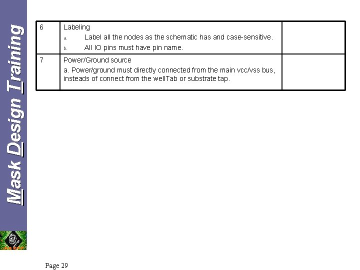
Mask Design Training 6 Labeling a. Label all the nodes as the schematic has and case-sensitive. b. All IO pins must have pin name. 7 Power/Ground source a. Power/ground must directly connected from the main vcc/vss bus, insteads of connect from the well. Tab or substrate tap. Page 29

Mask Design Training Q&A Page 30