MAPS readout Systems Christoph Schrader Dresden 26 09

- Slides: 17

MAPS readout Systems Christoph Schrader Dresden -26. 09. 2007

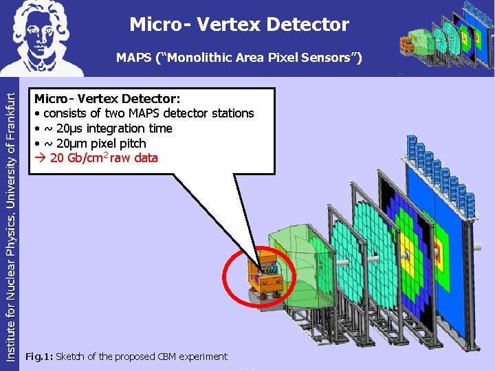
Micro- Vertex Detector MAPS (“Monolithic Area Pixel Sensors”) Micro- Vertex Detector: • consists of two MAPS detector stations • ~ 20µs integration time • ~ 20µm pixel pitch 20 Gb/cm 2 raw data Fig. 1: Sketch of the proposed CBM experiment

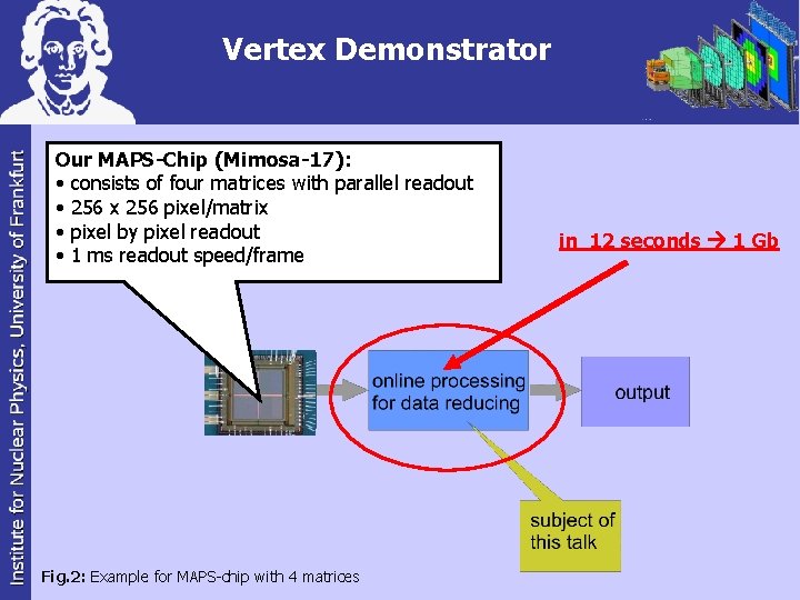
Vertex Demonstrator Our MAPS-Chip (Mimosa-17): • consists of four matrices with parallel readout • 256 x 256 pixel/matrix • pixel by pixel readout • 1 ms readout speed/frame Fig. 2: Example for MAPS-chip with 4 matrices in 12 seconds 1 Gb

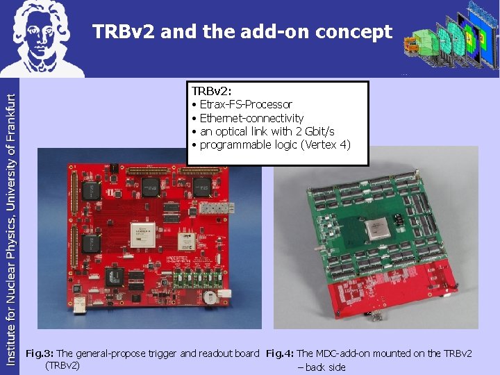
TRBv 2 and the add-on concept TRBv 2: • Etrax-FS-Processor • Ethernet-connectivity • an optical link with 2 Gbit/s • programmable logic (Vertex 4) Fig. 3: The general-propose trigger and readout board Fig. 4: The MDC-add-on mounted on the TRBv 2 (TRBv 2) – back side

Duties and responsibilities of the TRBv 2 for the MAPS add-on • High data-rate digital interface connector (15 Gbit/s) • FPGA configuration • High data transfer with optical link (2 Gbit/s) • Application process interface (API) • Power supply +5 V, 10 A • Clock distribution

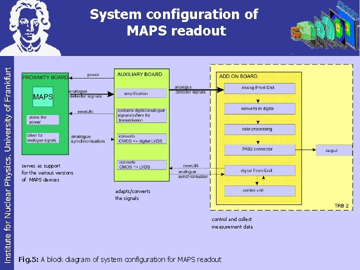
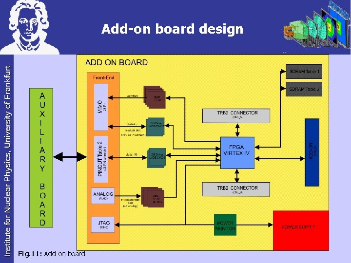
System configuration of MAPS readout serves as support for the various versions of MAPS devices adapts/converts the signals control and collect measurement data Fig. 5: A block diagram of system configuration for MAPS readout

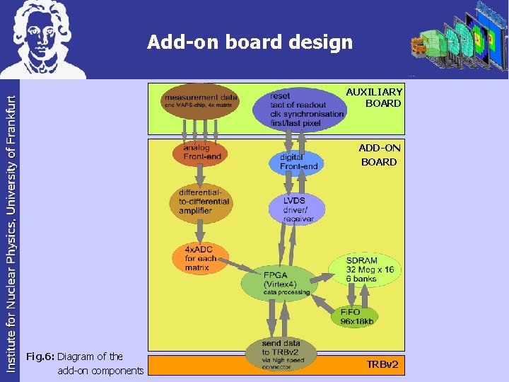
Add-on board design AUXILIARY BOARD ADD-ON BOARD Fig. 6: Diagram of the add-on components TRBv 2

Data processing • Correlated double sampling • Data compression • Threshold

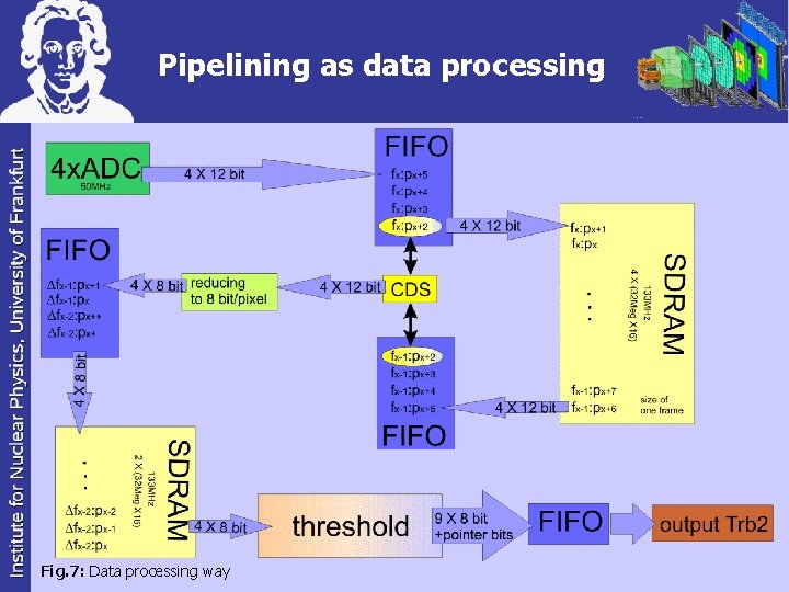
Pipelining as data processing Fig. 7: Data processing way

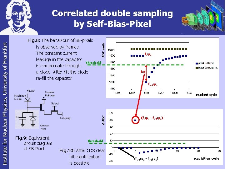
Correlated double sampling by Self-Bias-Pixel ADC units Fig. 8: The behaviour of SB-pixels is observed by frames. The constant current leakage in the capacitor threshold is compensate through a diode. After hit the diode re-fill the capacitor 1900 fx: px hit fx-1: px ∆ ADC readout cycle Fig. 9: Equivalent circuit diagram of SB-Pixel (fx: px - fx-1: px) threshold Fig. 10: After CDS clear hit identification is possible (fx-1: px - fx-2: px) acquisition cycle

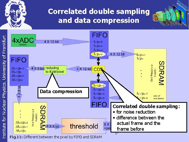
Correlated double sampling and data compression Data compression Correlated double sampling: • for noise reduction • difference between the actual frame and the frame before Fig. 11: Different between the pixel by FIFO and SDRAM

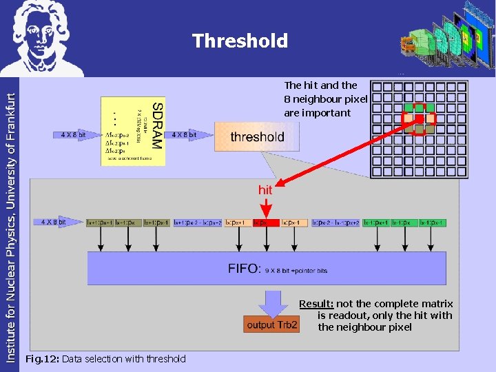
Threshold The hit and the 8 neighbour pixel are important Result: not the complete matrix is readout, only the hit with the neighbour pixel Fig. 12: Data selection with threshold

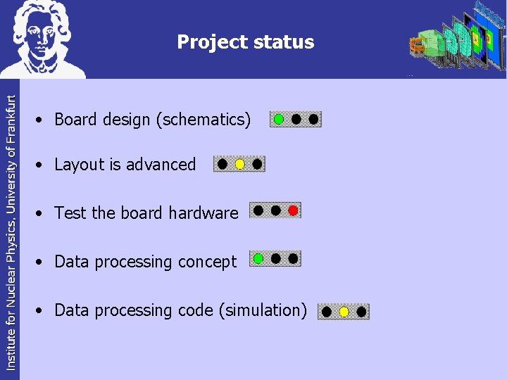
Project status • Board design (schematics) • Layout is advanced • Test the board hardware • Data processing concept • Data processing code (simulation)

THANK YOU

Add-on board design Fig. 11: Add-on board

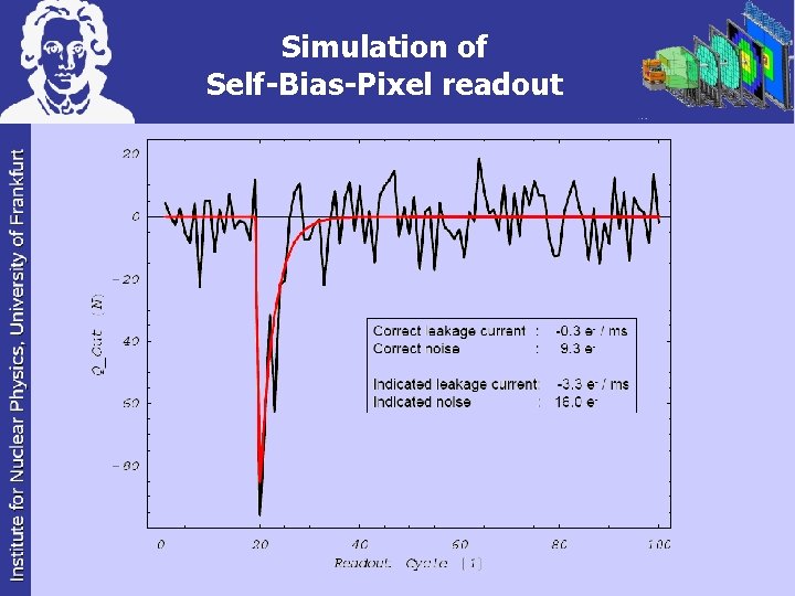
Simulation of Self-Bias-Pixel readout

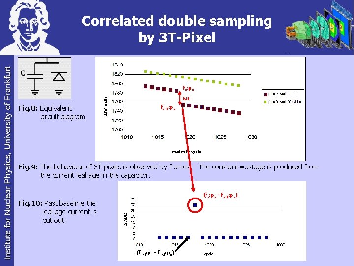
Correlated double sampling by 3 T-Pixel fx: px ADC units Fig. 8: Equivalent circuit diagram hit fx-1: px readouto cycle Fig. 9: The behaviour of 3 T-pixels is observed by frames. The constant wastage is produced from the current leakage in the capacitor. Fig. 10: Past baseline the leakage current is cut out ∆ ADC (fx: px - fx-1: px) (fx-1: px - fx-2: px) cycle