MAPLD 2004 DCDC Switching Power Converter with Radiation

- Slides: 1

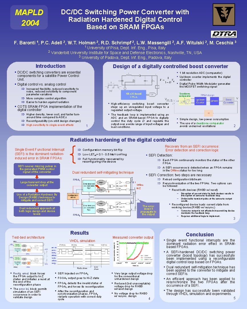
MAPLD 2004 DC/DC Switching Power Converter with Radiation Hardened Digital Control Based on SRAM FPGAs F. Baronti 1, P. C. Adell 2, W. T. Holman 2, R. D. Schrimpf 2, L. W. Massengill 2, A. F. Witulski 2, M. Ceschia 3 2 1 University of Pisa, Dept. Inf. Eng. , Pisa, Italy Vanderbilt University Institute for Space and Defense Electronics, Nashville, TN, USA 3 University of Padova, Dept. Inf. Eng. , Padova, Italy Introduction Design of a digitally controlled boost converter • DC/DC switching converters are essential • • components for a satellite Power Control Unit. Digital control vs. analog control Þ Increased flexibility, reduced sensitivity to noise, reduced sensitivity to component parameter variations More complex control algorithm Easier to harden against radiation Deadzone comparator Þ Þ • COTS SRAM-FPGA implementation of the digital controller Þ Higher density, lower cost, and faster turnÞ Þ around time compared to ASICs Reconfigurability (on-orbit design changes) High sensitivity to single event effects 1 bit resolution ADC (comparator) Up/down counter implements the digital controller Digital Pulse Width Modulator generates the MOSFET switching signal • High-efficiency switching boost converter steps up an unregulated input voltage to a regulated output voltage. • The feedback loop is implemented using an ADC and an SRAM-based FPGA to digitally control the duty cycle D and regulate the output over a wide range of input voltages and load conditions. 1 • • Simple design, low power consumption The use of a deadzone comparator avoids undesired oscillations 2 Radiation hardening of the digital controller Single Event Functional Interrupt (SEFI) is the dominant radiationinduced error in SRAM FPGAs: SEFI causes missing pulses in the generated PWM control signal of the converter Þ Þ Þ • SEFI Detection: Low LETth= 0. 1 - 0. 5 Me. V cm 2/mg Full functionality recovered by reconfiguring the device Þ Þ Dual redundant self-mitigating technique FPGA 1 Large transient drop at the converter output Recovery from an SEFI occurrence: Error detection and correction logic Configuration memory bit flip 1 • SEFI Correction: two steps are necessary Þ Þ 01 Offline 1 Hi-Z 10 1 0 Use of a Radiation Hardness By Design (RHBD) technique to mitigate and correct SEFI - 0 1 1 1 FPGA 2 Results Test-bed architecture Reload configuration bitstream Resynchronization of the two FPGAs. Two options can be followed: • Reset both devices (RHBD w/ reset) - Disruption of current state for both devices results in 1 1 Dual redundant approach at both logic design and device levels Each FPGA continuously monitors the status of the other FPGA A SEFI occurrence is detected when an FPGA remains in the Offline status for too long VHDL simulation • The error doesn’t propagate to the output Measured converter output • The error inj. block permits simulation of an SEFI occurrence in order to validate design • • • SEFI injected on FPGA 1 • After the reconfiguration and synchronization phases, FPGA 1 restarts operation with correct duty cycle • FGGA 1 output goes to Hi-Z state FPGA 2 detects the invalid status of FPGA 1 and forces its reconfiguration Very large output voltage drop for the conventional unhardened design • Reduced (but unacceptable) voltage drop for RHBD w/reset design • No voltage drop for RHBD w/ resync. design 4 maintains the feedback loop. Requires additional logic to implement. 3 Conclusion • Single event functional interrupts are the • Recfg. emul. block forces the FPGA output to hi-Z status and initiates a reset at the end of the reconfiguration phase Reconfigured device loads current state from working device (RHBD w/ resync. ) - Converter output is not affected since working device - • • interruption of converter feedback loop. Undesirable transient pulse at the converter output results. • • dominant radiation error effect in SRAMbased FPGAs. A SEFI-hardened DC/DC switching power converter (boost topology) has successfully been implemented using a reconfigurable digital control loop based on FPGAs. Dual redundant self-mitigation technique has been applied to the converter to mitigate and correct SEFIs. An efficient approach has been applied to resynchronize the two FPGAs after the occurrence of a SEFI. The design has successfully been validated through VHDL simulation and experiments. 5