MAKO A 350850 mm camera designed for operation










- Slides: 27

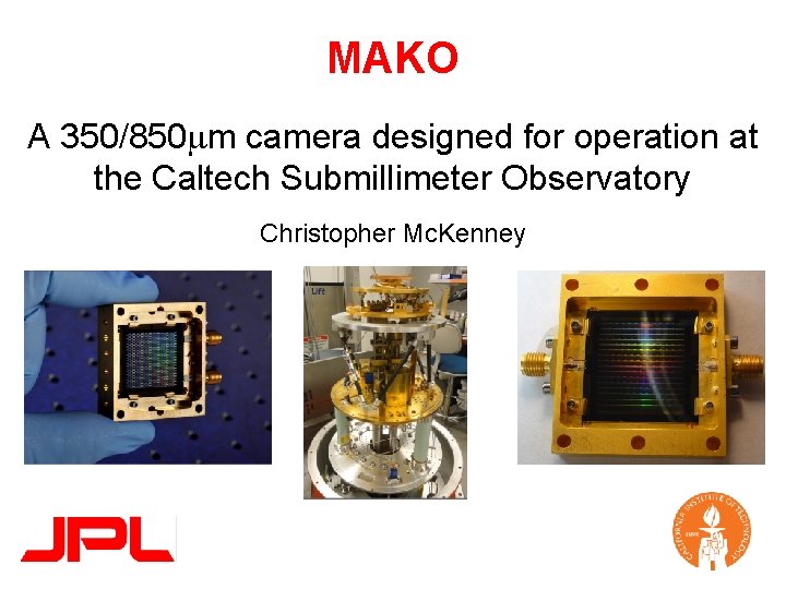
MAKO A 350/850 mm camera designed for operation at the Caltech Submillimeter Observatory Christopher Mc. Kenney

MAKO Technology Goals • SHARC-II already at CSO • 384 pixels • Background limited • Fills ~ ¼ of the focal plane Why MAKO? • Large-Scale Arrays (~ 105 pixels) • Pathfinder cameras for future telescopes such as CCAT • Current FIR technology has sufficient NEP • Need to significantly scale: • Readout/Multiplexing • Fabrication

MAKO: “Real” Goals • Filling large focal planes requires lots of pixels • Make fabrication and readout negligible parts of instrument cost • Our Goals: • < $1 / pixel: Fabrication • < $1 / pixel: Readout • Reasonable NEPs (with a clear path forward to improve) • TESes exist and have good NEPs – reasonable cost for ~ 100 – 1000 pixel arrays

MAKO Candidate Pixel Requirements Multiplexing • > 400 pixels / line • RF readout < 250 MHz Optics • F ~ 4. 5 • l = 350 mm • Pinc ~ 25 – 50 p. W Cryogenics • 3 He System • T ~ 240 m. K • One pair of RF lines Fabrication • High yield • Stepper Lithography • Ti. N superconductor

Low Cost Readout: Radio-Frequency Operation: MKIDs X FPGA implements digital channelizer for readout tone separation Microwave (GHz) readout requires up/down frequency conversion RF readout (< 500 MHz) allows “direct drive’’ with ADC/DAC – Reduces readout complexity and cost – Converters are typically 12 -bit, 500 MSPS (ADC < $200 ea) Microwave readout RF readout • • • L. Swenson, LTD-15

MAKO Readout • ROACH Readout – Open-source FPGA readout (CASPER/Berkeley) – Adopted existing hardware to meet observing date – Maximum readout frequency: 250 MHz • 500 MSPS ADC converters operating in 1 st Nyquist zone • MAKO implemented with ~ 500 pixels with one ADC and one DAC • FPGA firmware supports up to 4 k pixels per ROACH • FPGA firmware developed by R. Monroe/JPL

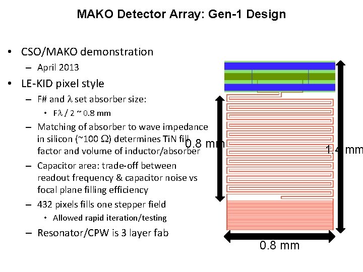
MAKO Detector Array: Gen-1 Design • CSO/MAKO demonstration – April 2013 • LE-KID pixel style – F# and l set absorber size: • Fl / 2 ~ 0. 8 mm – Matching of absorber to wave impedance in silicon (~100 W) determines Ti. N fill 0. 8 mm factor and volume of inductor/absorber – Capacitor area: trade-off between readout frequency & capacitor noise vs focal plane filling efficiency – 432 pixels fills one stepper field 1. 4 mm • Allowed rapid iteration/testing – Resonator/CPW is 3 layer fab 0. 8 mm

Ti. N + LE-KID Design: RF Frequency Operation Multiplexing requirement: frequencies < 250 MHz Ti. N: High resistivity superconductor High kinetic inductance = low frequency Leduc, et. al. APL 97 (102509) / 2010 • Adjustable Tc via N 2 during depostion • Achievable Tc ~ 0. 8 - 5 K • Meets cryogenic requirements (Tc ~ 1 K) • Long quasiparticle lifetime gives good optical response • Tc ~ 1 K, tqp ~ 100 ms • Lifetime appears to scale as Tc-2

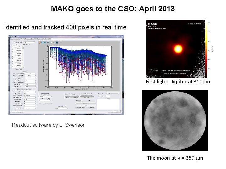
MAKO goes to the CSO: April 2013 Identified and tracked 400 pixels in real time First light: Jupiter at 350 mm Readout software by L. Swenson The moon at l = 350 mm

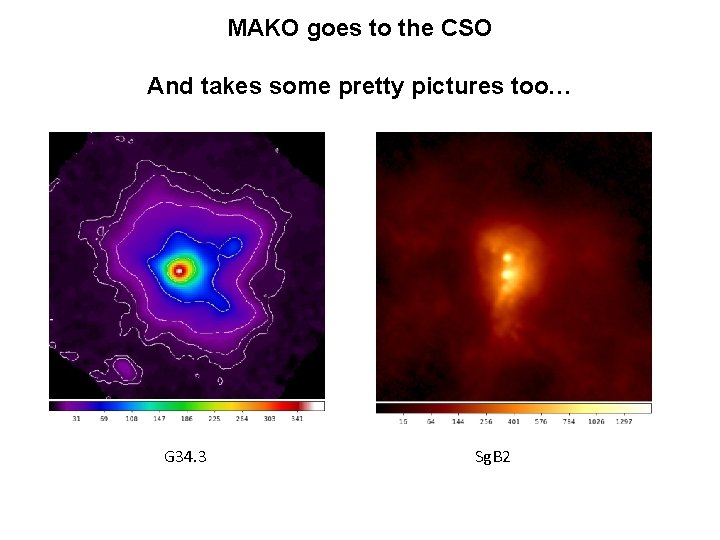
MAKO goes to the CSO And takes some pretty pictures too… G 34. 3 Sg. B 2

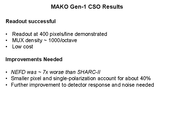
MAKO Gen-1 CSO Results Readout successful • Readout at 400 pixels/line demonstrated • MUX density ~ 1000/octave • Low cost Improvements Needed • NEFD was ~ 7 x worse than SHARC-II • Smaller pixel and single-polarization account for about 40% • Further improvement to detector response and noise needed

Goals for Aug/Sep 2014 CSO Run: • NEP Closer to BLIP • Polarization insenstivie (or dual-polarization) response • Mature readout • 350 micron / 850 micron detectors • Decided on an ambitious schedule to meet CCAT design deadlines and show on-sky performance • Why not make the fabrication even simpler?

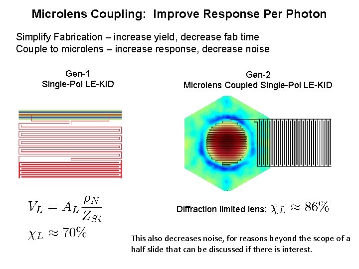
Microlens Coupling: Improve Response Per Photon Simplify Fabrication – increase yield, decrease fab time Couple to microlens – increase response, decrease noise Gen-1 Single-Pol LE-KID Gen-2 Microlens Coupled Single-Pol LE-KID Diffraction limited lens: This also decreases noise, for reasons beyond the scope of a half slide that can be discussed if there is interest.

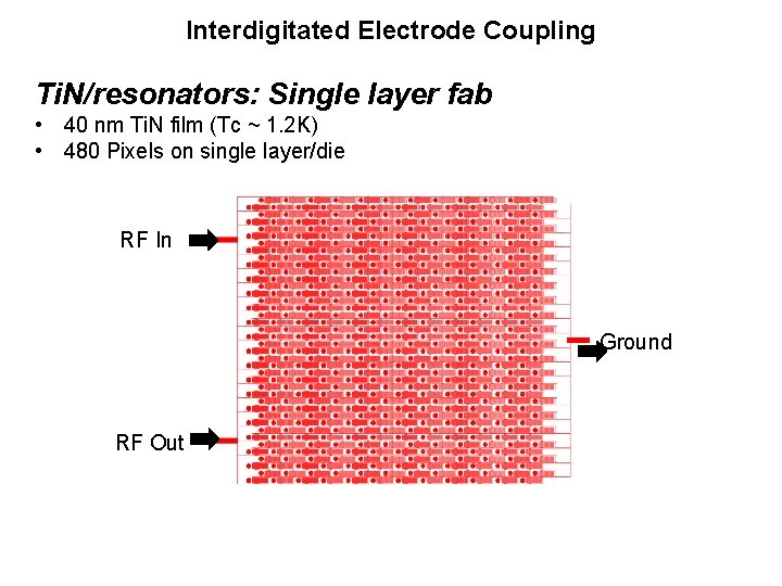
Simple Fabrication: Interdigitated Electrode Coupling IDE Coupling RF In RF Out • • 100 MHz in Si: l ~ 1 meter Treat elements as lumped In parallel with transmission line Rectangular RF feed pattern

Interdigitated Electrode Coupling Ti. N/resonators: Single layer fab • 40 nm Ti. N film (Tc ~ 1. 2 K) • 480 Pixels on single layer/die RF In Ground RF Out

Interdigitated Electrode Coupling Ti. N/resonators: Single layer fab • 40 nm Ti. N film (Tc ~ 1. 2 K) • 480 Pixels on single layer/die RF In Ground RF Out Lens Area = 1 mm 2

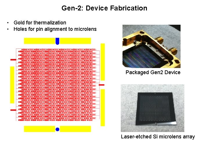
Gen-2: Device Fabrication • Gold for thermalization • Holes for pin alignment to microlens Packaged Gen 2 Device Laser-etched Si microlens array

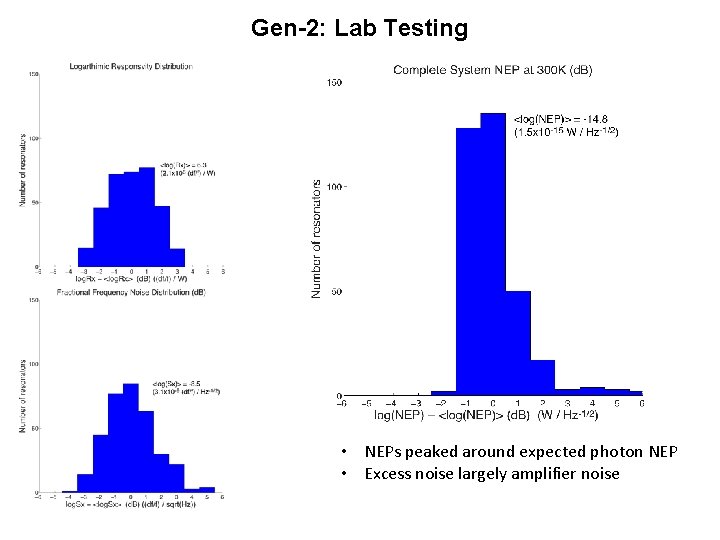
Gen-2: Improved noise and response • Many detectors appear to be near BLIP in lab • Excess noise at 300 K loading: 10 – 30% from amplifier • Read out all detectors simultaneously with ROACH readout

Gen-2: Lab Testing • NEPs peaked around expected photon NEP • Excess noise largely amplifier noise

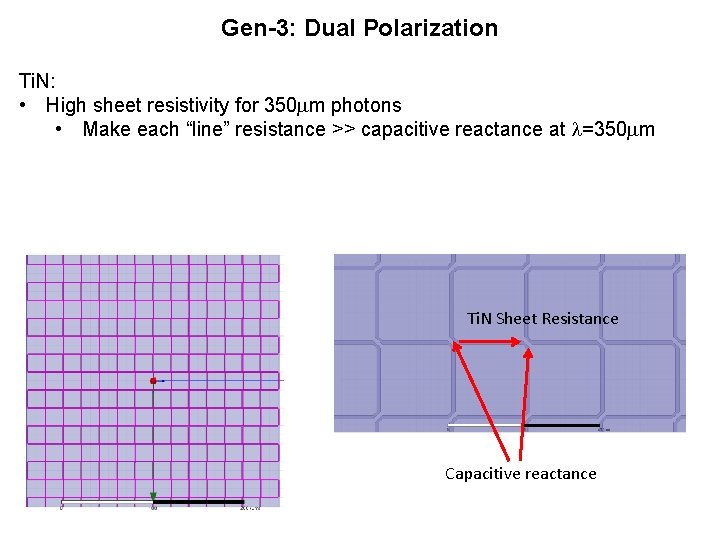
Gen-3: Dual Polarization Ti. N: • High sheet resistivity for 350 mm photons • Make each “line” resistance >> capacitive reactance at l=350 mm Ti. N Sheet Resistance Capacitive reactance

Gen-3: Dual Polarization Ti. N: • High sheet resistivity for 350 mm photons • Make each “line” resistance >> capacitive reactance at l=350 mm • Incident radiation sees Ti. N effective resistivity 350 um HFSS: > 95% absorption in both polarizations at 350 mm

Gen-3: Dual Polarization Ti. N: • High sheet resistivity for 350 mm photons • Make each “line” resistance >> capacitive reactance at l=350 mm • Incident radiation sees Ti. N effective resistivity • Superconductor at 100 MHz • Capacitive reactance large compared to inductive path RF Path

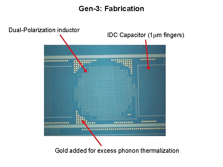
Gen-3: Fabrication Dual-Polarization inductor IDC Capacitor (1 mm fingers) Gold added for excess phonon thermalization

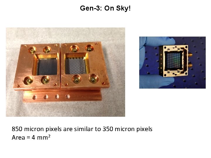
Gen-3: On Sky! 850 micron pixels are similar to 350 micron pixels Area = 4 mm 2

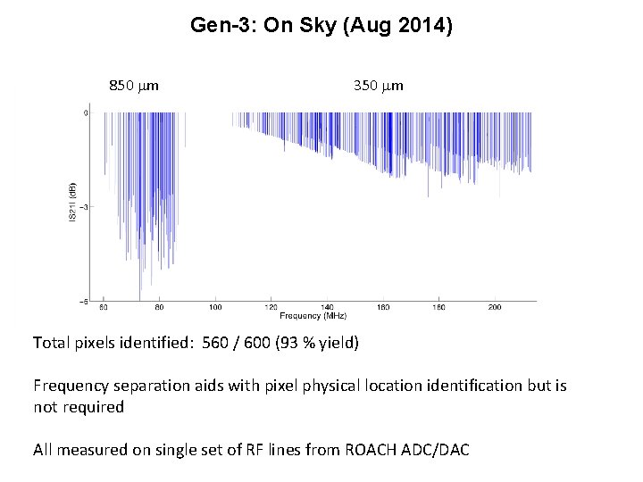
Gen-3: On Sky (Aug 2014) 850 mm 350 mm Total pixels identified: 560 / 600 (93 % yield) Frequency separation aids with pixel physical location identification but is not required All measured on single set of RF lines from ROACH ADC/DAC

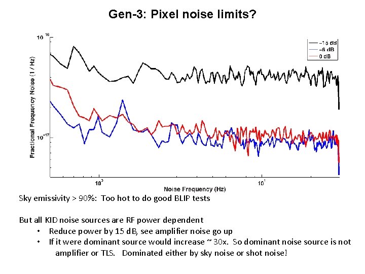
Gen-3: Pixel noise limits? Sky emissivity > 90%: Too hot to do good BLIP tests But all KID noise sources are RF power dependent • Reduce power by 15 d. B, see amplifier noise go up • If it were dominant source would increase ~ 30 x. So dominant noise source is not amplifier or TLS. Dominated either by sky noise or shot noise!

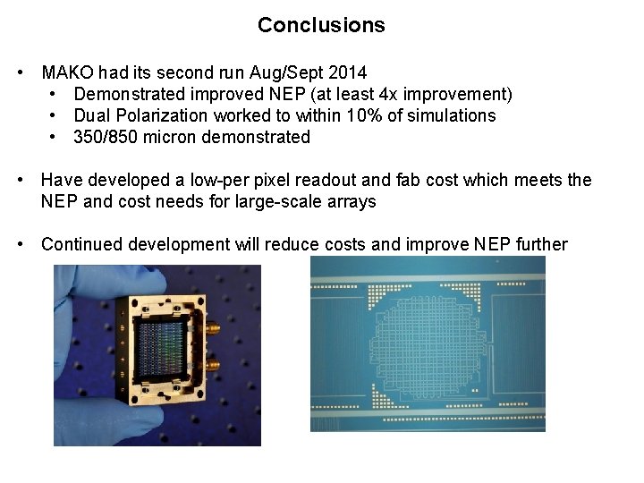
Conclusions • MAKO had its second run Aug/Sept 2014 • Demonstrated improved NEP (at least 4 x improvement) • Dual Polarization worked to within 10% of simulations • 350/850 micron demonstrated • Have developed a low-per pixel readout and fab cost which meets the NEP and cost needs for large-scale arrays • Continued development will reduce costs and improve NEP further