
Lumi Cal Towards electronics design Halina Abramowicz Ronen
Lumi. Cal Towards electronics design Halina Abramowicz, Ronen Ingbir, Sergey Kananov, Aharon Levy, Iftach Sadeh Tel Aviv University Collaboration High precision design FCAL -- TAU 22/11/2006 1
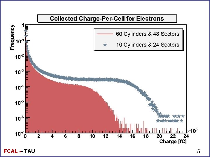
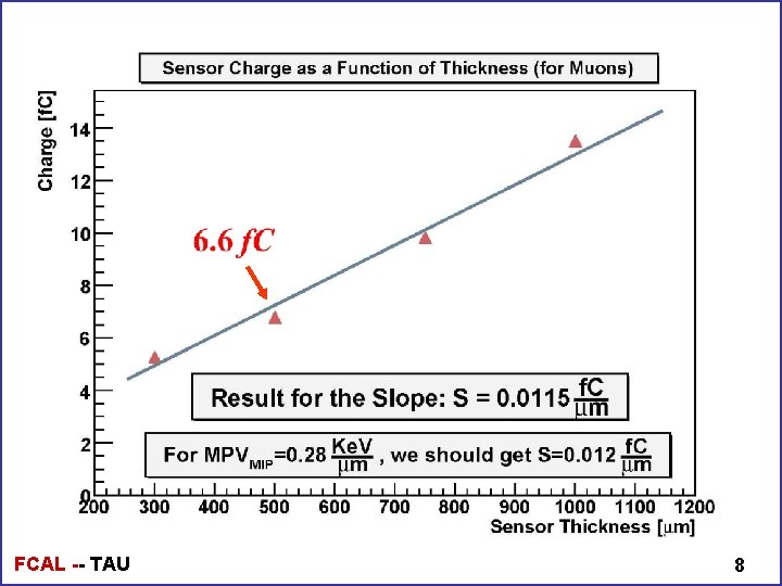
Signals in Units of Charge 1. Sensors Area 2. Sensors Thickness Physics Sample 1. 250 Ge. V MIPS (Muon sample) 2. 250 Ge. V electrons (contained EM showers) FCAL -- TAU 2
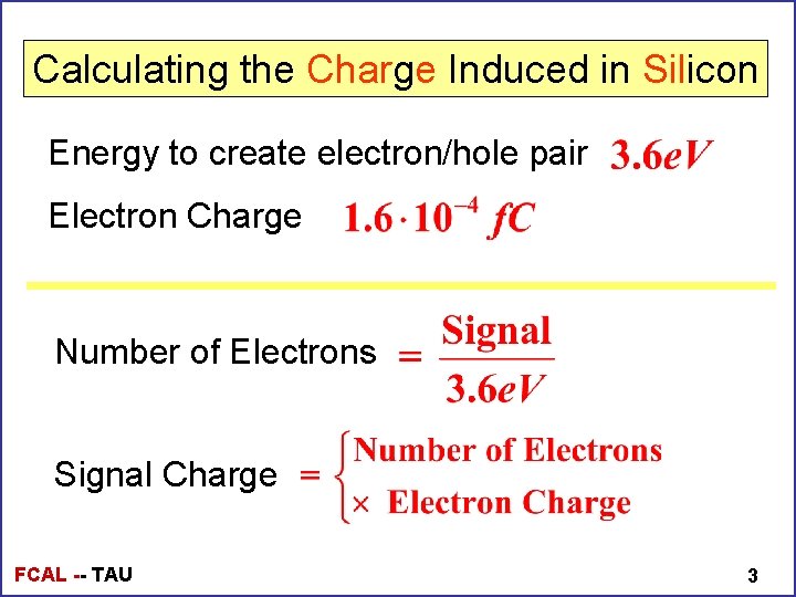
Calculating the Charge Induced in Silicon Energy to create electron/hole pair Electron Charge Number of Electrons Signal Charge FCAL -- TAU 3
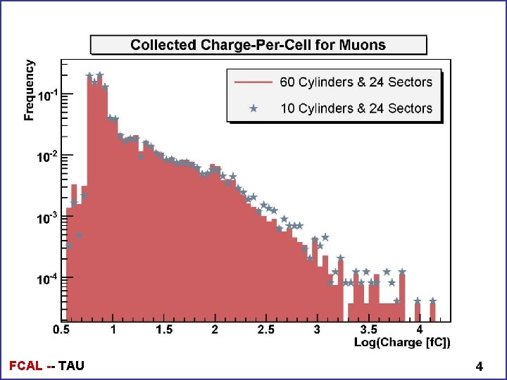
FCAL -- TAU 4
FCAL -- TAU 5
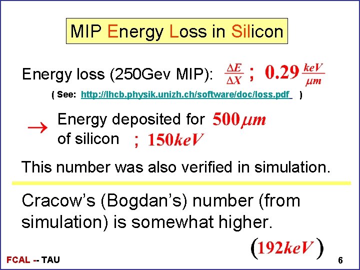
MIP Energy Loss in Silicon Energy loss (250 Gev MIP): ( See: http: //lhcb. physik. unizh. ch/software/doc/loss. pdf ) Energy deposited for of silicon This number was also verified in simulation. Cracow’s (Bogdan’s) number (from simulation) is somewhat higher. FCAL -- TAU 6
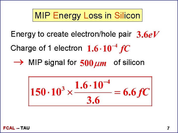
MIP Energy Loss in Silicon Energy to create electron/hole pair Charge of 1 electron MIP signal for FCAL -- TAU of silicon 7
FCAL -- TAU 8
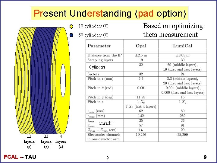
Present Understanding (pad option) Based on optimizing theta measurement 10 cylinders (θ) 60 cylinders (θ) Cylinders (mrad) 14 11 layers (z) FCAL -- TAU 15 4 layers (z) 9 9
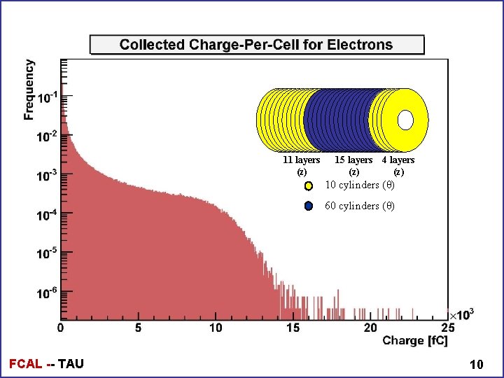
11 layers (z) 15 layers (z) 4 layers (z) 10 cylinders (θ) 60 cylinders (θ) FCAL -- TAU 10
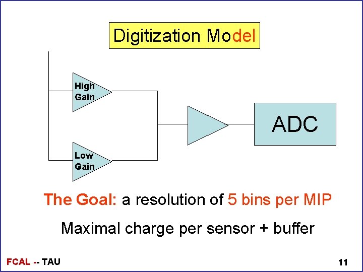
Digitization Model High Gain ADC Low Gain The Goal: a resolution of 5 bins per MIP Maximal charge per sensor + buffer FCAL -- TAU 11
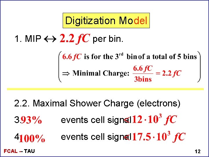
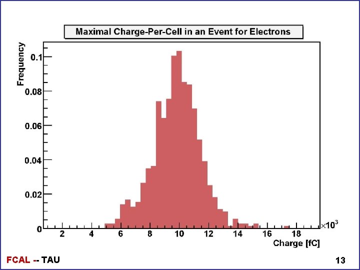
Digitization Model 1. MIP per bin. 2. 2. Maximal Shower Charge (electrons) 3. events cell signal 4. events cell signal FCAL -- TAU 12
FCAL -- TAU 13
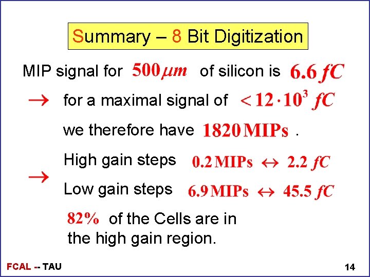
Summary – 8 Bit Digitization MIP signal for of silicon is for a maximal signal of we therefore have . High gain steps Low gain steps of the Cells are in the high gain region. FCAL -- TAU 14
- Slides: 14