LSILSI L W tox Scaling DeviceCircuit parameter Scaling


 DRAM混載にするとこの部分の消費電力が大幅に削減できる。 MPEG 4 codec 高速信号はチップ外に出してはいけない! DRAM Separate chips DRAM on a")
 # of operations/clock Operating speed (GOPS) Pd (m. W)")
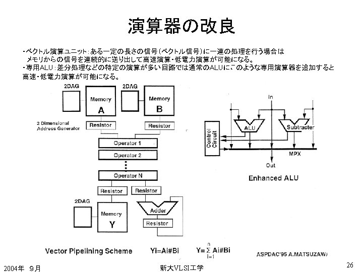
 ME LM VLC LM VLD LM")


 Interconnection delay Gate delay Design Rule (um) 2004年 9月")


 349 254 90 163")
 配線の種類による動作周波数限界 100 G Module (1 Clock) Local (1/4 clock) Module")
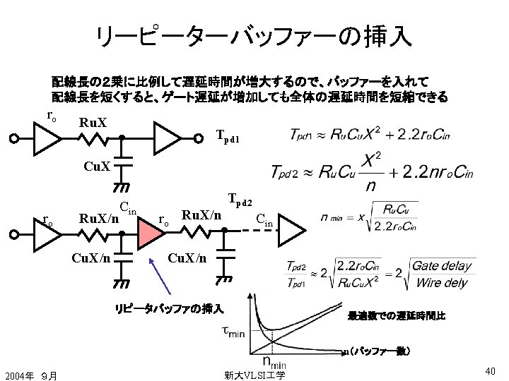
 リピーターバッファの効果 100 G Above chip 10 G Global 2 4")
![参考文献 [References] [1] K. Ueda, T. Sugimura, et. al. , "A 16 -bit Digital](https://slidetodoc.com/presentation_image_h/a78310516561a175b547bc91a829168b/image-50.jpg "参考文献 [References] [1] K. Ueda, T. Sugimura, et. al. , \"A 16 -bit Digital")

- Slides: 51
LSI技術の黄金則:スケーリング則はLSIの黄金則である L W tox Scaling Device/Circuit parameter Scaling Factor Device dimensions L, W, Tox 1/S Doping concentration S~S 1. 5 Voltage 1/S Field 1 Current 1/S Gate Delay 1/S Power dissipation/device 1/S 3~ 1/S 2 動作電圧も1/Sにする 微細化・低電圧化により、 ・高密度化(低コスト) ・高速化 ・低消費電力 が同時に達成される R. H. Dennard, et al. , IEEE, JSC, SC-9, p. 256, 1974. 不純物濃度を上げるのは空乏層厚を下げるためである。 2004年 9月 新大VLSI 学 6
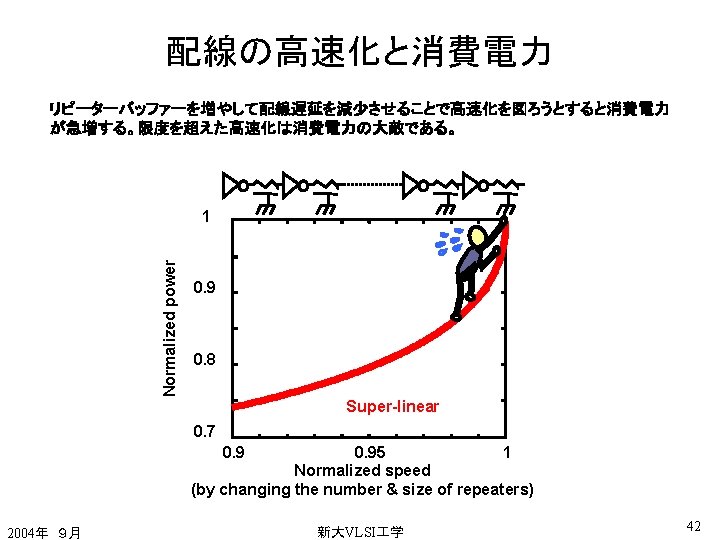
Power reduction: Example Power dissipation can be reduced to 1/10 Clock circuit consumes power of 75% of total Pd in this LSI. Power consumption (A. U) F/F reduction Gated CLK 100 80 60 Clock 75 1/2 30. 5 40 Interconnect 20 0 2004年 9月 Volt. lowering 3. 0 V->1. 5 V Cap. Lowering (0. 6) 18 7 Macro 13 6. 5 1/5 8 3 1 2 1. 7 3 0. 35 um 0. 18 um 新大VLSI 学 19
DRAM混載による低消費電力化 外付けDRAMはI/O部分で電力を消費する。(内蔵メモリーの 100倍程度) DRAM混載にするとこの部分の消費電力が大幅に削減できる。 MPEG 4 codec 高速信号はチップ外に出してはいけない! DRAM Separate chips DRAM on a chip Logic & memory DRAM - logic 891 m. W interface VT Speech codec 16 Mbit DRAM 240 m. W Host I/F Multiplexer DRAM I/F Power 70% power reduction by DRAM embedding alone Courtesy Toshiba, ISSCC 2000 2004年 9月 VT 新大VLSI 学 MPEG-4 Video Cam Pre. Display PLL Codec I/F filter VT VT 20
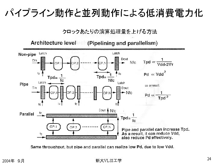
LSIアーキテクチャによる演算速度と消費電力差 LSIアーキテクチャにより消費電力/演算速度は3桁の違いがある!! Clock frequency (MHz) # of operations/clock Operating speed (GOPS) Pd (m. W) Operating speed (GOPS) CPU DSP Dedicated LSI 450 50 25 2 16 96 0. 9 0. 8 2. 4 7000 110 12 7800 138 5 Pd/GOPS: 3 orders 2004年 9月 新大VLSI 学 25
MPEG 4 LSIの構成 DSPに各種ビデオコーディック専用回路を付加させた VCE (Video Codec Engines) ME LM VLC LM VLD LM DCT IDCT PAD LM PNR Programmable DSP Inst. DSP Core Mem Data Mem CAD LM COMP HIF (Host I/F) MIF (Memory I/F) DRAM (2 Mb) Main Sub Graph. Filter DRAM (2 Mb) DRAM (16 Mb) VPU(Video Processing Unit) Video Input 2004年 9月 Video Output 新大VLSI 学 27
Performance for Core Decoding 画像Codecでは専用演算器を設けて演算処理速度を向上できる。 Decoding Performance : 5 fps HW Engine Software CAD 6. 1% PAD 26. 5% 6. 8% COMP 63% Texture Decoding Kcycles 0 5 WITH the Engines Core@L 1 Decoding 40 WITHOUT the Engines 24% 0 2004年 9月 20 fps Mcycles 100 新大VLSI 学 200 28
クロックゲーティングの効果 使用しない回路へのクロックを停止するとこで大幅な低電力化が可能 ØThe Effect of Clock Gating 40% Non Clock Gating 100 0 300 [m. W] 200 ØThe Effect of Core Engines WITH the Core Engines 37% WITHOUT the Core Engines 100 0 DSP 2004年 9月 VCE (Core) 300 [m. W] 200 VCE (not Core) VPU 新大VLSI 学 MIF DRAM PAD 29
電源電圧制御 Vdd固定ではクロック周波数を下げたときに消費電力は比例でしか変化しないが 遅くても良い処理の場合はクロック周波数を下げるとともにVddも下げる。 こうすると大幅に消費電力が低減できる。 Energy consumption is proportional to the square of VDD should be lowered to the minimum level which ensures the real-time operation. 2004年 9月 Normalized energy 1. 0 0. 8 Variable Vdd Fixed Vdd 0. 6 0. 4 0. 2 0. 0 新大VLSI 学 Long channel (a=2) Short channel (a=1. 3) 0. 2 0. 4 0. 6 0. 8 Normalized workload 1. 0 30
電圧ホッピング リアルタイム画像エンコードを電圧ホッピングにより電力 1/10を達成 MPEG-4 video encoding 0. 16 Normalized Power P/PFIX 0. 14 0. 12 0. 10 RVH: 2 levels (f, f/2) RVH : 3 levels (f, f/2, f/3) RVH : 4 levels (f, f/2, f/3, f/4) RVH : infinite levels post-simulation analysis 0. 08 0. 06 0. 04 VDD 0. 02 0. 00 0. 0 SH-4 0. 2 0. 4 0. 6 0. 8 1. 0 Transition Delay TTD (ms) S. Lee and T. Sakurai, “Run-time Power Control Scheme Using Software Feedback Loop for Low-Power Real-time Applications, ”ASPDAC'00, A 5. 2, pp. 381~pp. 386, Jan. 2000. S. Lee and T. Sakurai, “Run-time Voltage Hopping for Low-power Real-time Systems, ” DAC'00, June 2000. 2004年 9月 新大VLSI 学 VDD Modified Clock SH-4 Clock 31
Vddによるリーク電流制御 電源電圧Vddを高くするとDIBL効果によりVTが下がりリーク電流が多くなる。 そこで、遅くても良い回路ブロックのVddを下げることによりリーク電流を下げることができる。 1 Normalized power Source Changing VDD alone 0. 8 Surface potential 0. 6 VDS 0. 4 0. 2 PDYNAMIC Super-linear PLEAK (without DIBL) PLEAK (with DIBL) 0 0 0. 5 1 s=0. 1 V/decade VTH/VDD, MAX=0. 15 Normalized speed 2004年 9月 Drain 新大VLSI 学 32
ゲート遅延と配線遅延 ゲート遅延は減少しているが配線遅延は増加している。 500 Delay time (ps) Interconnection delay Gate delay Design Rule (um) 2004年 9月 新大VLSI 学 T. Mogami “LP & HS LSI Circuit & Technology” pp. 547 -560, Realize Inc. 1998. 39
Technology roadmap グローバル配線遅延はたとえ、リピータバッファを入れても微細化とともに増大する。 Insertion of repeater ITRS 2001 Edition, pp. 261. Global w/ repeater Repeater buffer Local Gate 2004年 9月 新大VLSI 学 41
配線長分布 短い配線は多く、長い配線は少ない。 階層的な多層配線技術の導入 Interconnect Density Function 106 Theoretical Curve 105 104 103 L = (142, 742)1/2 = 377 [gate pitch] Actual Data Number of gate N=142, 742 p = 0. 8 k = 5. 0 102 101 100 10 -1 1 10 Lower layer: high density (Hi RC) Upper layer: low density (Lo RC) Chip length L 1000 Interconnect Length [Unit in Gate Pitch] Davis, De, and Meindl, IEEE ED-45(3) 580 (1998) 2004年 9月 新大VLSI 学 43
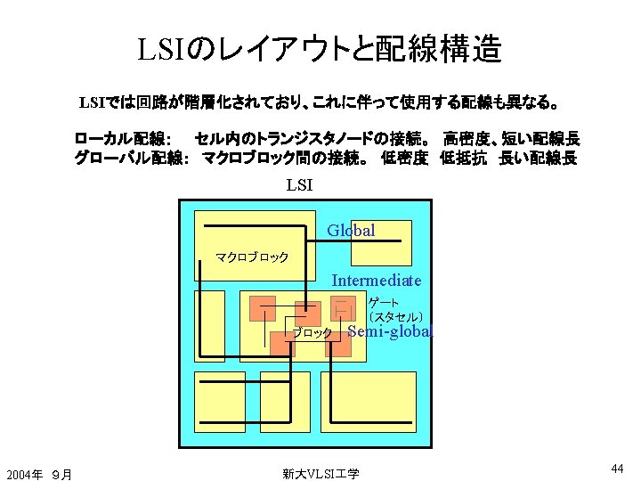
階層配線 Current LSI technology uses hierarchical interconnection structure. Global interconnection uses thicker and wider metals. 2 x to 3 x ITRS 2001 Edition, pp. 262. 2004年 9月 新大VLSI 学 45
現在のSo. C用多層配線 Current LSI uses hierarchical Cu interconnection technology, however the parameter ratio between Global and local is small. Ratio: 2 x 2004年 9月 新大VLSI 学 46
配線の検討 Local Global Above chip Module PWB C (f. F/mm) 349 254 90 163 113 Rsq(Ohm/mm) 455 227 100 0. 01 0. 005 RC (ps/mm) 159 57. 7 9. 02 0. 0016 0. 00057 L (n. H/mm) ---- 1. 05 0. 47 W (um) 0. 22 0. 44 1 60 100 h (um) 0. 34 1 60 35 d (um) 0. 20 0. 40 1 60 100 H (um) 0. 79 3. 02 3000 180 2004年 9月 新大VLSI 学 47
Maximum operating frequency (Hz) 配線の種類による動作周波数限界 100 G Module (1 Clock) Local (1/4 clock) Module (1/4 Clock) 10 G LC barrier Delay condition 1 G PWB Local 100 M Attenuation condition Global Above chip 10 M 0. 1 1 10 100 Wire length (mm) 2004年 9月 新大VLSI 学 48
Maximum operating frequency (Hz) リピーターバッファの効果 100 G Above chip 10 G Global 2 4 4 Buffer inserted (tpd=20 ps) 5 1 G 9 9 11 Local 14 100 M Non-inserted 15 10 M 0. 1 1 10 100 Wire length (mm) 2004年 9月 新大VLSI 学 49
参考文献 [References] [1] K. Ueda, T. Sugimura, et. al. , "A 16 -bit Digital Signal Processor with Specially Arranged Multiply. Accumulator for Low Power Consumption, " IEICE�Transaction, Vol. E 78 -C, No. 12, pp. 1709 -1716, 1995. [2] K. Honma and O. Kato, "Trends of research and development in Europe and America, " Journal of The IEICE, Vol. 78, no. 2, pp. 173 -178, 1995. [3] H. Kabuo, M. Okamoto, et. al. , "An 80 MOPS-Peak High-Speed and Low-Power-Consumption 16 -bit Digital Signal Processor, " IEEE JSSC, Vol. 31, No. 4, pp. 494 -503, 1996. [4] A. P. Chandrakasan, S. Sheng, et. al. , "Low-power CMOS digital design, " IEEE JSSC, Vol. 27, No. 4, pp. 473 -484, 1992. [5] I. Verbauwhede and M. Touriguian, "Low Power DSP Engine for Wireless Communications, " Journal of VLSI Signal Processing 18, pp. 177 -186, 1998. [6] N. Nakajima, H. Shibata, et al. , "Baseband System LSI for Cellular Mobile Telephone, " Matsushita Technical Journal, pp. 46 -52, 1999. [7] M. Okamoto K. Stone, et. al. , "A High Performance DSP Architecture for Next Generation Mobile Phone Systems, " IEEE DSP Workshop, 1998. [8] T. Ishikawa, H. Suzuki, et al. , "W-CDMA hardware-related issues, " IEEE ICCT, 1998. [9] S. Kurohmaru, M. Matsuo, et. al. , "A MPEG 4 Programmable Codec DSP with an Embedded Pre/Postprocessing Engine, " IEEE CICC, 1999. 2004年 9月 新大VLSI 学 50
参考文献 • J. M. Rabaey and M. Pedram, “Low Power Design Methodologies, ” Kuluwer. • K. Roy and S. C. Prasad, “Low-Power CMOS VLSI Circuit Design, ” Wiley-interscience. • 「低電力LSIの技術白書」日経BP • 桜井貴康監修 「低消費電力、高速LSI技術」 リアライズ社 • T. Hashimoto, et al. , “A 90 m. W MPEG 4 Video Codec LSI with the Capability for Core Profile, ” ISSCC 2001, 9. 1. 2004年 9月 新大VLSI 学 51