LowPower IC Design Gating Techniques TsungChu Huang Dept



![Clock Gating Options • set_clock_gating_style – – – [-sequential_cell latch | none] [-minimum_bitwidth_value] [-setup_value] Clock Gating Options • set_clock_gating_style – – – [-sequential_cell latch | none] [-minimum_bitwidth_value] [-setup_value]](https://slidetodoc.com/presentation_image_h/131b0c8764aee13533ecacf596a881a3/image-37.jpg)
![Dual-Speed LFSR [3] • They separate the LFSR-like RTPG into a slower part S Dual-Speed LFSR [3] • They separate the LFSR-like RTPG into a slower part S](https://slidetodoc.com/presentation_image_h/131b0c8764aee13533ecacf596a881a3/image-50.jpg)
![Low-Transition RTPG [4] • Assume the LFSR can generate 2 r patterns including 0 Low-Transition RTPG [4] • Assume the LFSR can generate 2 r patterns including 0](https://slidetodoc.com/presentation_image_h/131b0c8764aee13533ecacf596a881a3/image-51.jpg)
![Analyses [4] • They analyze the probability of a consecutive pattern segment for k=2 Analyses [4] • They analyze the probability of a consecutive pattern segment for k=2](https://slidetodoc.com/presentation_image_h/131b0c8764aee13533ecacf596a881a3/image-52.jpg)
![Properties of LT-LFSR [4] • Assigning identical values to neighboring inputs may decrease fault Properties of LT-LFSR [4] • Assigning identical values to neighboring inputs may decrease fault](https://slidetodoc.com/presentation_image_h/131b0c8764aee13533ecacf596a881a3/image-53.jpg)
![Experimental Results[4] • Results for k=2 (3) are listed, 14~35% (23~59%) transition reductions are Experimental Results[4] • Results for k=2 (3) are listed, 14~35% (23~59%) transition reductions are](https://slidetodoc.com/presentation_image_h/131b0c8764aee13533ecacf596a881a3/image-54.jpg)

![Switching Activity Masking Technique[1] • • Using a NOR (NAND) to mask Q by Switching Activity Masking Technique[1] • • Using a NOR (NAND) to mask Q by](https://slidetodoc.com/presentation_image_h/131b0c8764aee13533ecacf596a881a3/image-63.jpg)
![Decoding Exhaustive Patterns as TPG[1] • Deterministic patterns are selected by a PLA-like decoder Decoding Exhaustive Patterns as TPG[1] • Deterministic patterns are selected by a PLA-like decoder](https://slidetodoc.com/presentation_image_h/131b0c8764aee13533ecacf596a881a3/image-65.jpg)
![Peak-Power Reduction by Partitioning [2] • Basic Concept: The transversals of justification and propagation Peak-Power Reduction by Partitioning [2] • Basic Concept: The transversals of justification and propagation](https://slidetodoc.com/presentation_image_h/131b0c8764aee13533ecacf596a881a3/image-66.jpg)
![Partitioning by Mux/De. Mux Inserting[2] • The boundary wires are separated by inserting multiplexers Partitioning by Mux/De. Mux Inserting[2] • The boundary wires are separated by inserting multiplexers](https://slidetodoc.com/presentation_image_h/131b0c8764aee13533ecacf596a881a3/image-67.jpg)
![Multilevel Graph Bisection Algorithm[2] • Coarsening because some nodes cannot be separated, e. g. Multilevel Graph Bisection Algorithm[2] • Coarsening because some nodes cannot be separated, e. g.](https://slidetodoc.com/presentation_image_h/131b0c8764aee13533ecacf596a881a3/image-68.jpg)
![Experimental Results[2] and Comments • Average Reduction Percentages of 14 Circuits: – – Peak Experimental Results[2] and Comments • Average Reduction Percentages of 14 Circuits: – – Peak](https://slidetodoc.com/presentation_image_h/131b0c8764aee13533ecacf596a881a3/image-69.jpg)







![On/Off Current Ratio Ø Ion/Ioff trades delay cost with leakage reduction [ISCA 02 Heo], On/Off Current Ratio Ø Ion/Ioff trades delay cost with leakage reduction [ISCA 02 Heo],](https://slidetodoc.com/presentation_image_h/131b0c8764aee13533ecacf596a881a3/image-108.jpg)


- Slides: 128

Low-Power IC Design Gating Techniques Tsung-Chu Huang Dep’t of Electronic Eng. , Nat’l Changhua Univ. Spring 2007 Low-Power IC Design. Tsung-Chu Huang, NCUE Ch. 9 Power-Gating 1 NCUE EDAT

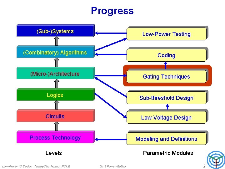
Progress (Sub-)Systems Low-Power Testing (Combinatory) Algorithms Coding (Micro-)Architecture Gating Techniques Logics Sub-threshold Design Circuits Low-Voltage Design Process Technology Modeling and Definitions Levels Parametric Modules Low-Power IC Design. Tsung-Chu Huang, NCUE Ch. 9 Power-Gating 2 NCUE EDAT

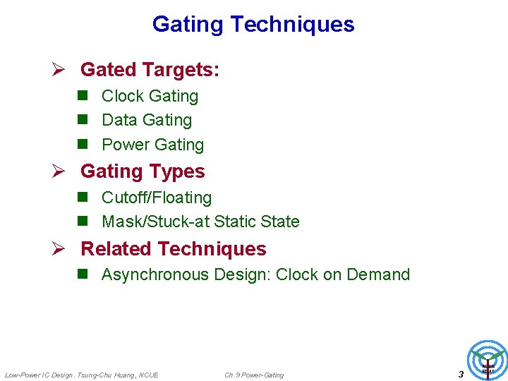
Gating Techniques Ø Gated Targets: n Clock Gating n Data Gating n Power Gating Ø Gating Types n Cutoff/Floating n Mask/Stuck-at Static State Ø Related Techniques n Asynchronous Design: Clock on Demand Low-Power IC Design. Tsung-Chu Huang, NCUE Ch. 9 Power-Gating 3 NCUE EDAT

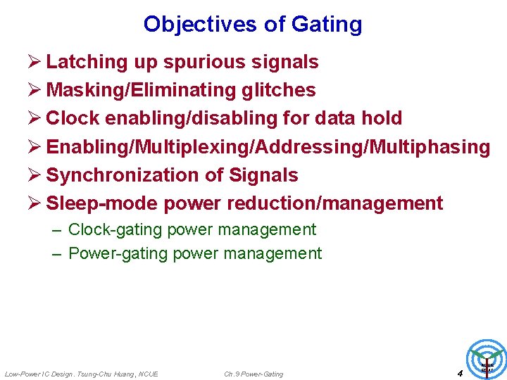
Objectives of Gating Ø Latching up spurious signals Ø Masking/Eliminating glitches Ø Clock enabling/disabling for data hold Ø Enabling/Multiplexing/Addressing/Multiphasing Ø Synchronization of Signals Ø Sleep-mode power reduction/management – Clock-gating power management – Power-gating power management Low-Power IC Design. Tsung-Chu Huang, NCUE Ch. 9 Power-Gating 4 NCUE EDAT

Clock Gating Low-Power IC Design. Tsung-Chu Huang, NCUE Ch. 9 Power-Gating 5 NCUE EDAT

Outline of Clock Gating • • • Model Review on Latches and Flipflops Clock-Domains Issues Progress on Clock Gating Flow Guide and Check Low-Power IC Design. Tsung-Chu Huang, NCUE Ch. 9 Power-Gating 6 NCUE EDAT

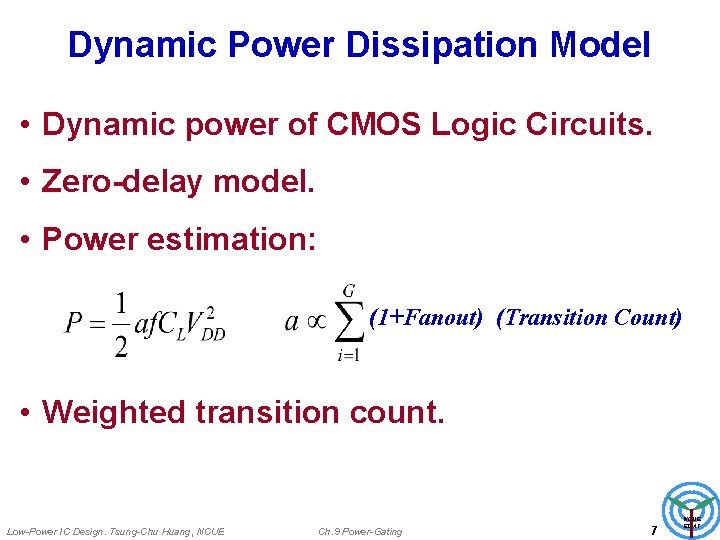
Dynamic Power Dissipation Model • Dynamic power of CMOS Logic Circuits. • Zero-delay model. • Power estimation: (1+Fanout) (Transition Count) • Weighted transition count. Low-Power IC Design. Tsung-Chu Huang, NCUE Ch. 9 Power-Gating 7 NCUE EDAT

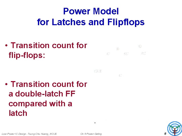
Power Model for Latches and Flipflops • Transition count for flip-flops: • Transition count for a double-latch FF compared with a latch Low-Power IC Design. Tsung-Chu Huang, NCUE Ch. 9 Power-Gating 8 NCUE EDAT

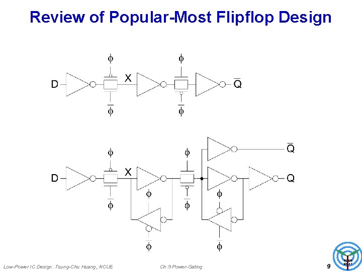
Review of Popular-Most Flipflop Design Low-Power IC Design. Tsung-Chu Huang, NCUE Ch. 9 Power-Gating 9 NCUE EDAT

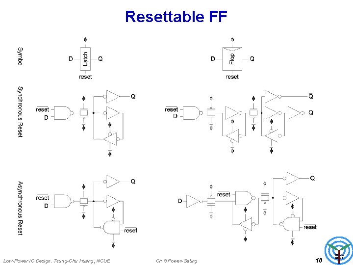
Resettable FF Low-Power IC Design. Tsung-Chu Huang, NCUE Ch. 9 Power-Gating 10 NCUE EDAT

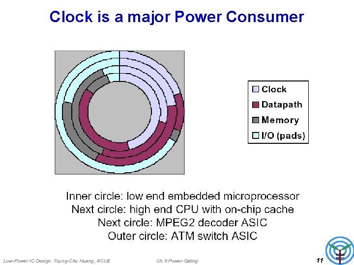
Clock is a major Power Consumer Low-Power IC Design. Tsung-Chu Huang, NCUE Ch. 9 Power-Gating 11 NCUE EDAT

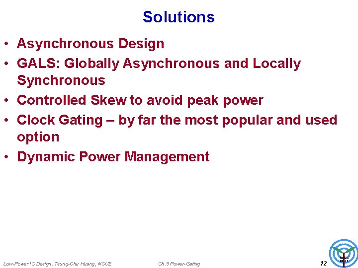
Solutions • Asynchronous Design • GALS: Globally Asynchronous and Locally Synchronous • Controlled Skew to avoid peak power • Clock Gating – by far the most popular and used option • Dynamic Power Management Low-Power IC Design. Tsung-Chu Huang, NCUE Ch. 9 Power-Gating 12 NCUE EDAT

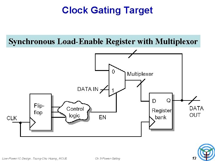
Clock Gating Target Synchronous Load-Enable Register with Multiplexor Low-Power IC Design. Tsung-Chu Huang, NCUE Ch. 9 Power-Gating 13 NCUE EDAT

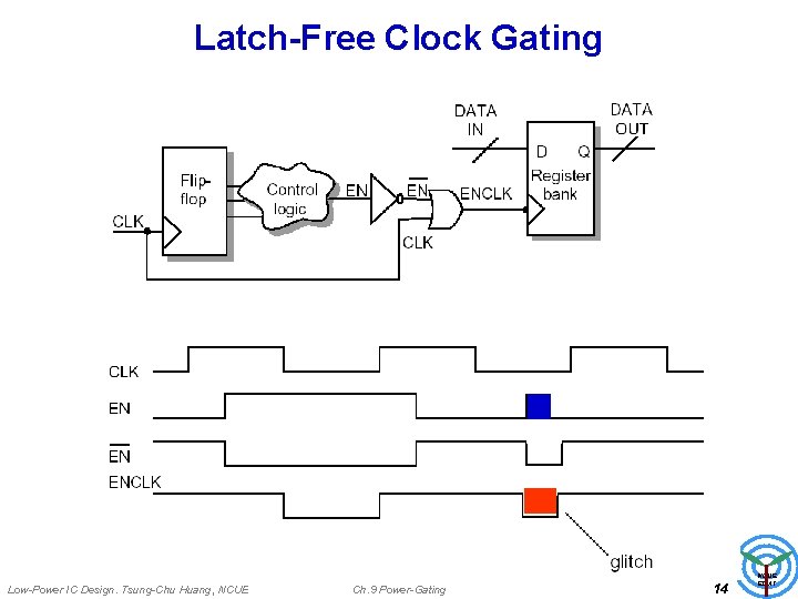
Latch-Free Clock Gating Low-Power IC Design. Tsung-Chu Huang, NCUE Ch. 9 Power-Gating 14 NCUE EDAT

Automatic Clock Gating Reduced Net Switching No Mux Reduced Internal Power Glitch-free Low-Power IC Design. Tsung-Chu Huang, NCUE Ch. 9 Power-Gating 15 NCUE EDAT

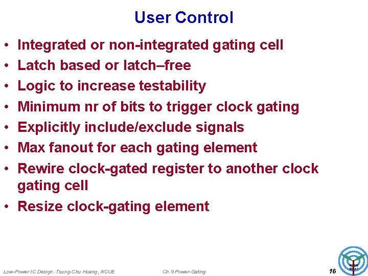
User Control • • Integrated or non-integrated gating cell Latch based or latch–free Logic to increase testability Minimum nr of bits to trigger clock gating Explicitly include/exclude signals Max fanout for each gating element Rewire clock-gated register to another clock gating cell • Resize clock-gating element Low-Power IC Design. Tsung-Chu Huang, NCUE Ch. 9 Power-Gating 16 NCUE EDAT

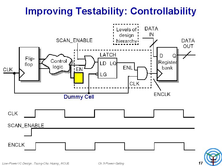
Improving Testability: Controllability Dummy Cell Low-Power IC Design. Tsung-Chu Huang, NCUE Ch. 9 Power-Gating 17 NCUE EDAT

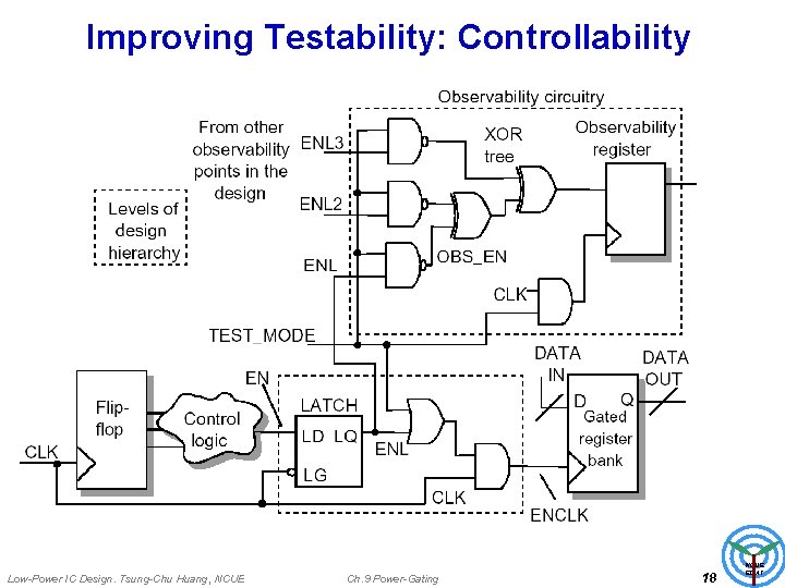
Improving Testability: Controllability Low-Power IC Design. Tsung-Chu Huang, NCUE Ch. 9 Power-Gating 18 NCUE EDAT

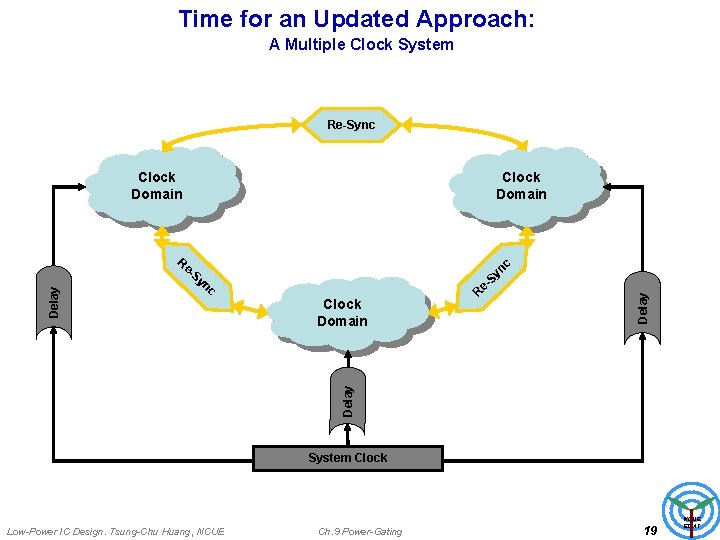
Time for an Updated Approach: A Multiple Clock System Re-Sync Clock Domain R nc nc e y -S Clock Domain R Delay Sy Delay e- System Clock Low-Power IC Design. Tsung-Chu Huang, NCUE Ch. 9 Power-Gating 19 NCUE EDAT

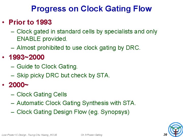
Progress on Clock Gating Flow • Prior to 1993 – Clock gated in standard cells by specialists and only ENABLE provided. – Almost prohibited to use clock gating by DRC. • 1993~2000 – Guide to Clock Gating. – Skip picky DRC but check by STA. • 2000~ – Clock Gating Cells – Automatic Clock Gating Synthesis with STA. – Clock Gating Design Flow (eg. Synopsys) Low-Power IC Design. Tsung-Chu Huang, NCUE Ch. 9 Power-Gating 20 NCUE EDAT

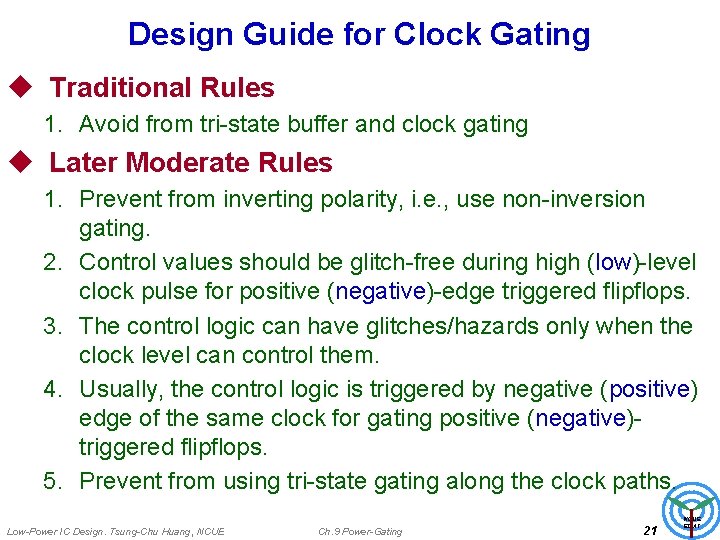
Design Guide for Clock Gating u Traditional Rules 1. Avoid from tri-state buffer and clock gating u Later Moderate Rules 1. Prevent from inverting polarity, i. e. , use non-inversion gating. 2. Control values should be glitch-free during high (low)-level clock pulse for positive (negative)-edge triggered flipflops. 3. The control logic can have glitches/hazards only when the clock level can control them. 4. Usually, the control logic is triggered by negative (positive) edge of the same clock for gating positive (negative)triggered flipflops. 5. Prevent from using tri-state gating along the clock paths. Low-Power IC Design. Tsung-Chu Huang, NCUE Ch. 9 Power-Gating 21 NCUE EDAT

Clock-Gating Cells for Synthesis E L K D Q G C I D Q Label Signal 0 1 C Regular Clock ↓ ↑ I Inversion Type Non-inverted Inverted K Gated Clock ↓ ↑ L Latch Type Low-level High-level G Gate Type OR AND E Enable/Disable Enable Low-Power IC Design. Tsung-Chu Huang, NCUE Ch. 9 Power-Gating Rule I = C⊕K L = ~C G=E 22 NCUE EDAT

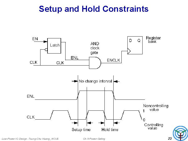
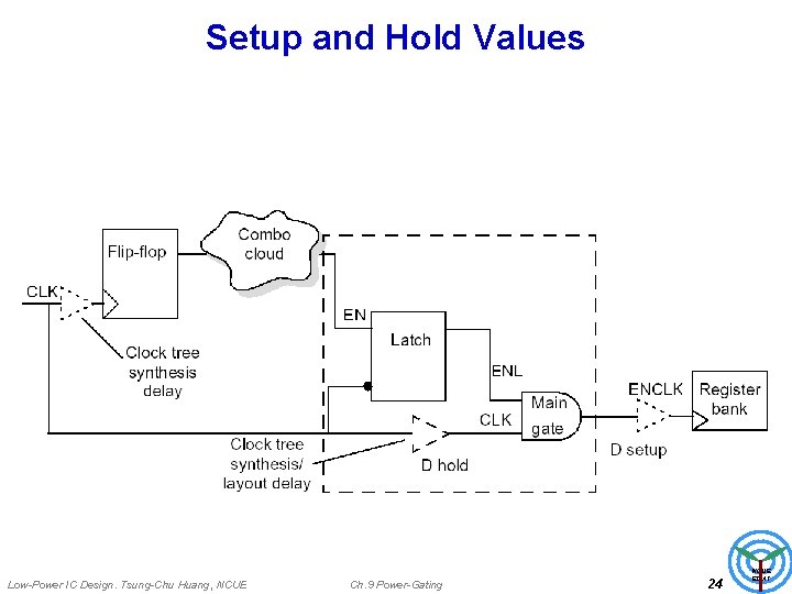
Setup and Hold Constraints Low-Power IC Design. Tsung-Chu Huang, NCUE Ch. 9 Power-Gating 23 NCUE EDAT

Setup and Hold Values Low-Power IC Design. Tsung-Chu Huang, NCUE Ch. 9 Power-Gating 24 NCUE EDAT

Glitch Elimination • Glitch-Free Design – Need for glitch free handshaking logic. • Clock-Domain Synchronization – Re-synchronization of cross-clock domain signals. • Adapting Data: Synchronizer and Iterface • Adapting Clock: PLL and SMD • STA: – A more sophisticated static timing analysis tool flow with multi-clock multi -mode capability. Low-Power IC Design. Tsung-Chu Huang, NCUE Ch. 9 Power-Gating 25 NCUE EDAT

Glitch Free Logic Why do we need glitch free components? Ø Clock Generation: l To create glitch free clocks and clock like signals i. e. STROBE for ram writes, IRQ for interrupts … Ø Avoid Contention: l To avoid tri-state bus contention during the enable/disable boundaries of multiple drivers. Ø Clock gating Ø Power dissipation reduction l Glitch Power takes about 20% of Average Power Dissipation. Ø EMI reduction l F=Ldi/dt Low-Power IC Design. Tsung-Chu Huang, NCUE Ch. 9 Power-Gating 26 NCUE EDAT

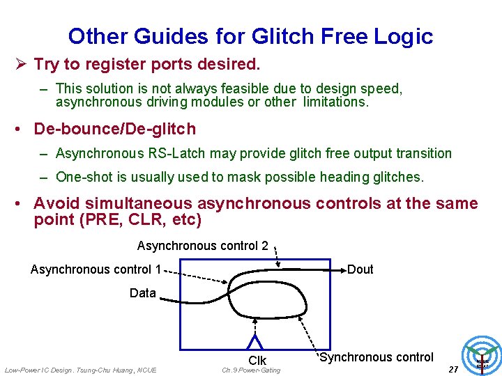
Other Guides for Glitch Free Logic Ø Try to register ports desired. – This solution is not always feasible due to design speed, asynchronous driving modules or other limitations. • De-bounce/De-glitch – Asynchronous RS-Latch may provide glitch free output transition – One-shot is usually used to mask possible heading glitches. • Avoid simultaneous asynchronous controls at the same point (PRE, CLR, etc) Asynchronous control 2 Asynchronous control 1 Dout Data Low-Power IC Design. Tsung-Chu Huang, NCUE Clk Ch. 9 Power-Gating Synchronous control 27 NCUE EDAT

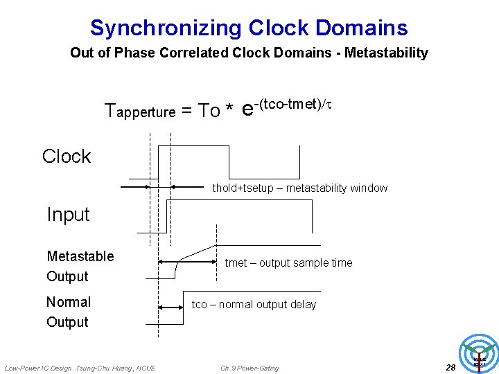
Synchronizing Clock Domains Out of Phase Correlated Clock Domains - Metastability Tapperture = To * e-(tco-tmet)/t Clock thold+tsetup – metastability window Input Metastable Output Normal Output Low-Power IC Design. Tsung-Chu Huang, NCUE tmet – output sample time tco – normal output delay Ch. 9 Power-Gating 28 NCUE EDAT

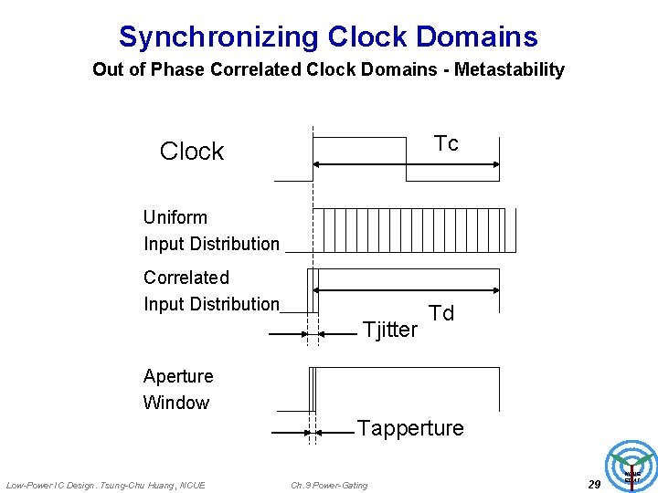
Synchronizing Clock Domains Out of Phase Correlated Clock Domains - Metastability Tc Clock Uniform Input Distribution Correlated Input Distribution Tjitter Td Aperture Window Tapperture Low-Power IC Design. Tsung-Chu Huang, NCUE Ch. 9 Power-Gating 29 NCUE EDAT

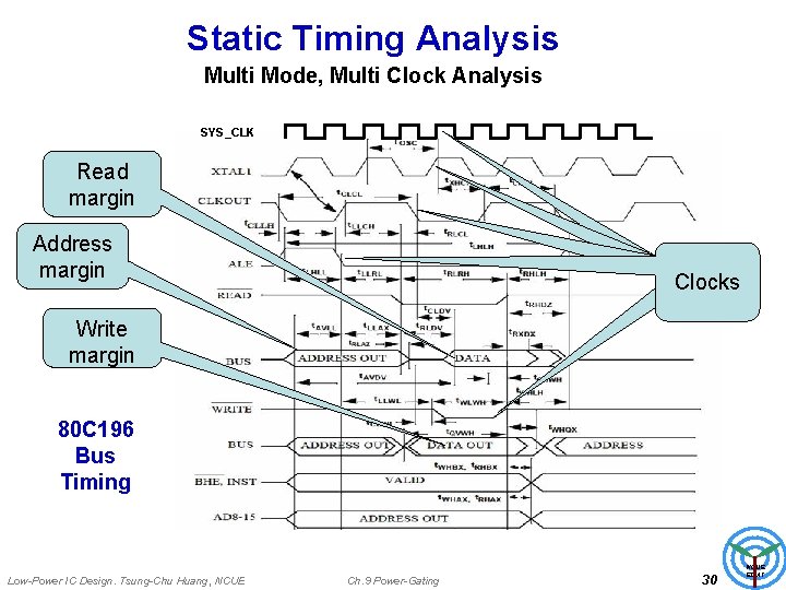
Static Timing Analysis Multi Mode, Multi Clock Analysis SYS_CLK Read margin Address margin Clocks Write margin 80 C 196 Bus Timing Low-Power IC Design. Tsung-Chu Huang, NCUE Ch. 9 Power-Gating 30 NCUE EDAT

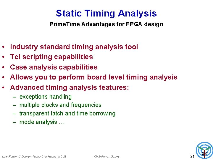
Static Timing Analysis Prime. Time Advantages for FPGA design • • • Industry standard timing analysis tool Tcl scripting capabilities Case analysis capabilities Allows you to perform board level timing analysis Advanced timing analysis features: – – exceptions handling multiple clocks and frequencies transparent latch and time borrowing mode analysis … Low-Power IC Design. Tsung-Chu Huang, NCUE Ch. 9 Power-Gating 31 NCUE EDAT

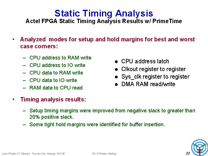
Static Timing Analysis Actel FPGA Static Timing Analysis Results w/ Prime. Time • Analyzed modes for setup and hold margins for best and worst case corners: – – – CPU address to RAM write CPU address to IO write CPU data to RAM write CPU data to IO write RAM data to CPU read l l CPU address latch Clkout register to register Sys_clk register to register DMA RAM read/write • Timing analysis results: – Setup timing margins were improved from negative slack to greater than 20% positive slack. – Some tight hold margins were identified for buffer insertion. Low-Power IC Design. Tsung-Chu Huang, NCUE Ch. 9 Power-Gating 32 NCUE EDAT

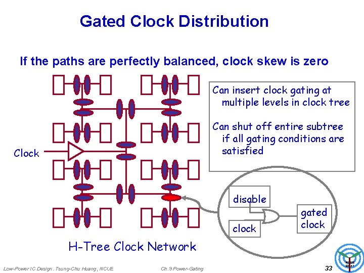
Gated Clock Distribution If the paths are perfectly balanced, clock skew is zero Can insert clock gating at multiple levels in clock tree Can shut off entire subtree if all gating conditions are satisfied Clock disable clock gated clock H-Tree Clock Network Low-Power IC Design. Tsung-Chu Huang, NCUE Ch. 9 Power-Gating 33 NCUE EDAT

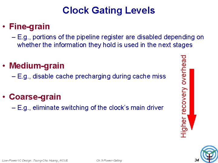
Clock Gating Levels • Fine-grain • Medium-grain – E. g. , disable cache precharging during cache miss • Coarse-grain – E. g. , eliminate switching of the clock’s main driver Low-Power IC Design. Tsung-Chu Huang, NCUE Ch. 9 Power-Gating Higher recovery overhead – E. g. , portions of the pipeline register are disabled depending on whether the information they hold is used in the next stages 34 NCUE EDAT

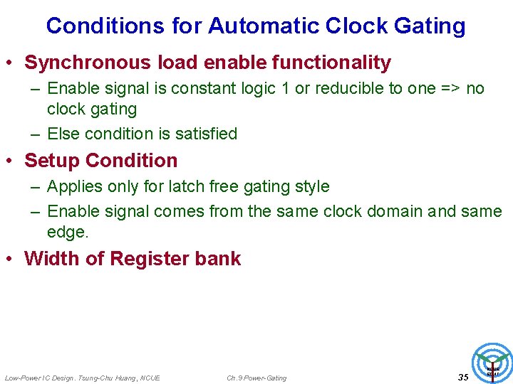
Conditions for Automatic Clock Gating • Synchronous load enable functionality – Enable signal is constant logic 1 or reducible to one => no clock gating – Else condition is satisfied • Setup Condition – Applies only for latch free gating style – Enable signal comes from the same clock domain and same edge. • Width of Register bank Low-Power IC Design. Tsung-Chu Huang, NCUE Ch. 9 Power-Gating 35 NCUE EDAT

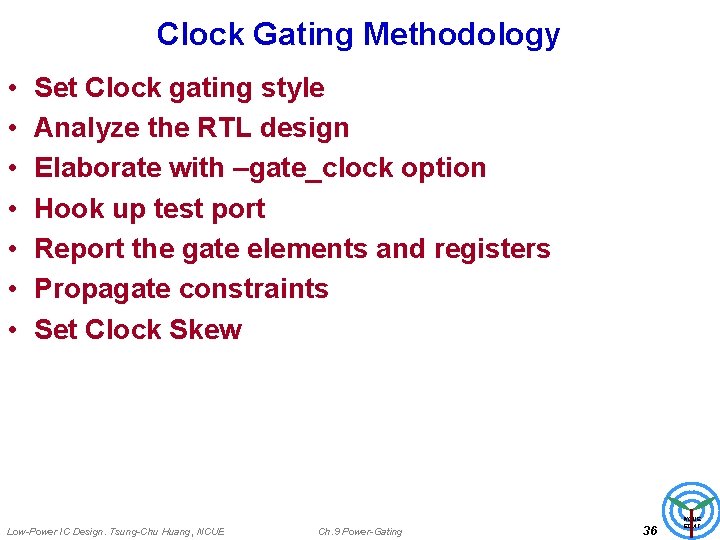
Clock Gating Methodology • • Set Clock gating style Analyze the RTL design Elaborate with –gate_clock option Hook up test port Report the gate elements and registers Propagate constraints Set Clock Skew Low-Power IC Design. Tsung-Chu Huang, NCUE Ch. 9 Power-Gating 36 NCUE EDAT
![Clock Gating Options setclockgatingstyle sequentialcell latch none minimumbitwidthvalue setupvalue Clock Gating Options • set_clock_gating_style – – – [-sequential_cell latch | none] [-minimum_bitwidth_value] [-setup_value]](https://slidetodoc.com/presentation_image_h/131b0c8764aee13533ecacf596a881a3/image-37.jpg)
Clock Gating Options • set_clock_gating_style – – – [-sequential_cell latch | none] [-minimum_bitwidth_value] [-setup_value] [-hold_value] [-positive_edge_logic { gate_list | integrated}] [-negative_edge_logic { gate_list | integrated}] [-control_point none | before | after] [-control_signal scan_enable | test_mode] [-observation_point true | false] [-observation_logic_depth_value] [-max_fanout_count] [-no_sharing] Low-Power IC Design. Tsung-Chu Huang, NCUE Ch. 9 Power-Gating 37 NCUE EDAT

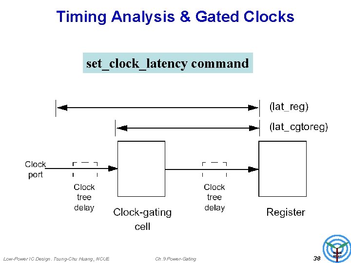
Timing Analysis & Gated Clocks set_clock_latency command Low-Power IC Design. Tsung-Chu Huang, NCUE Ch. 9 Power-Gating 38 NCUE EDAT

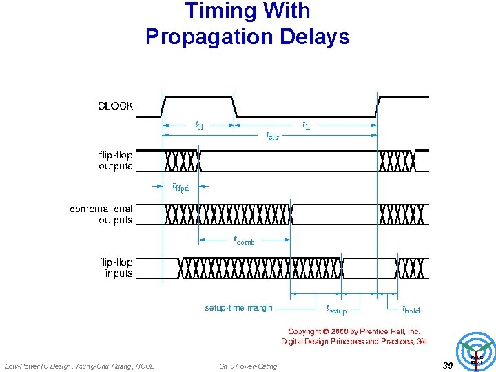
Timing With Propagation Delays Low-Power IC Design. Tsung-Chu Huang, NCUE Ch. 9 Power-Gating 39 NCUE EDAT

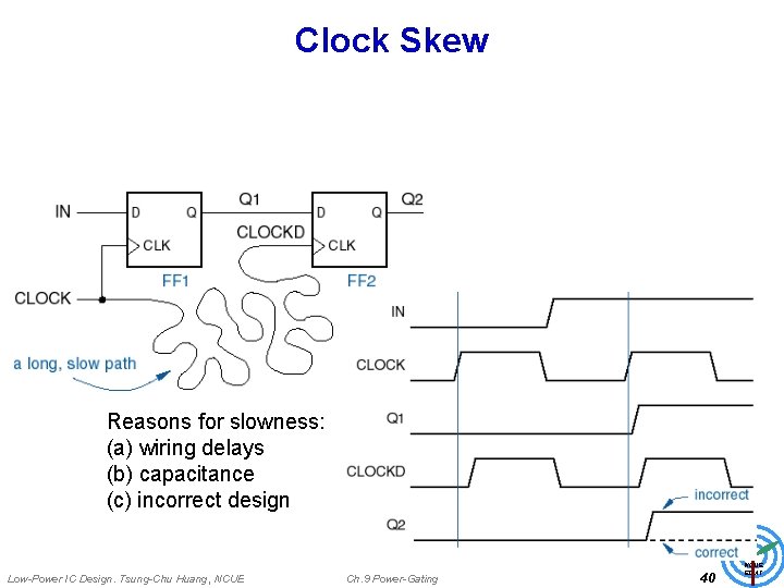
Clock Skew Reasons for slowness: (a) wiring delays (b) capacitance (c) incorrect design Low-Power IC Design. Tsung-Chu Huang, NCUE Ch. 9 Power-Gating 40 NCUE EDAT

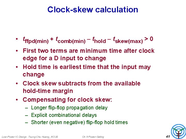
Clock-skew calculation • tffpd(min) + tcomb(min) - thold - tskew(max) > 0 • First two terms are minimum time after clock edge for a D input to change • Hold time is earliest time that the input may change • Clock skew subtracts from the available hold-time margin • Compensating for clock skew: – Longer flip-flop propagation delay – Explicit combinational delays – Shorter (even negative) flip-flop hold times Low-Power IC Design. Tsung-Chu Huang, NCUE Ch. 9 Power-Gating 41 NCUE EDAT

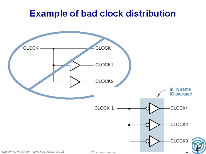
Example of bad clock distribution Low-Power IC Design. Tsung-Chu Huang, NCUE Ch. 9 Power-Gating 42 NCUE EDAT

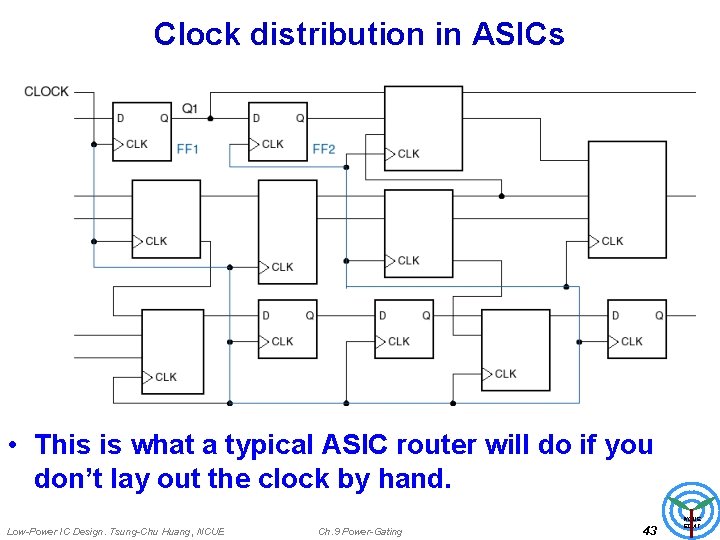
Clock distribution in ASICs • This is what a typical ASIC router will do if you don’t lay out the clock by hand. Low-Power IC Design. Tsung-Chu Huang, NCUE Ch. 9 Power-Gating 43 NCUE EDAT

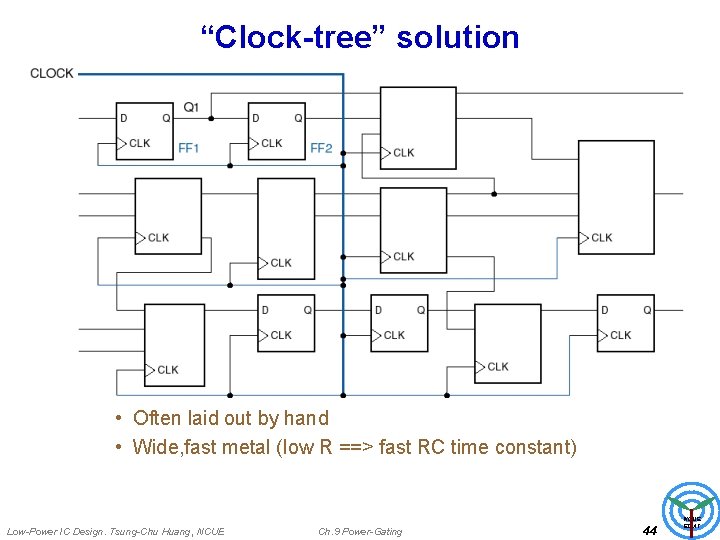
“Clock-tree” solution • Often laid out by hand • Wide, fast metal (low R ==> fast RC time constant) Low-Power IC Design. Tsung-Chu Huang, NCUE Ch. 9 Power-Gating 44 NCUE EDAT

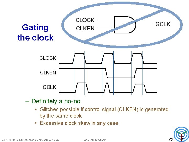
Gating the clock – Definitely a no-no • Glitches possible if control signal (CLKEN) is generated by the same clock • Excessive clock skew in any case. Low-Power IC Design. Tsung-Chu Huang, NCUE Ch. 9 Power-Gating 45 NCUE EDAT

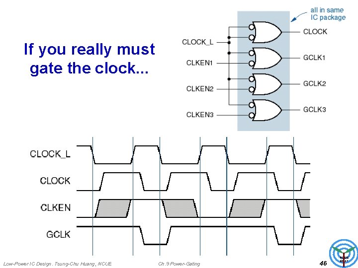
If you really must gate the clock. . . Low-Power IC Design. Tsung-Chu Huang, NCUE Ch. 9 Power-Gating 46 NCUE EDAT

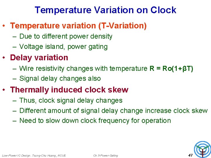
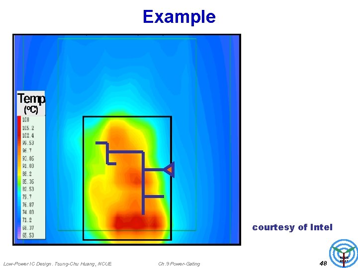
Temperature Variation on Clock • Temperature variation (T-Variation) – Due to different power density – Voltage island, power gating • Delay variation – Wire resistivity changes with temperature R = Ro(1+βT) – Signal delay changes also • Thermally induced clock skew – Thus, clock signal delay changes – Different amount of signal delay change increase clock skew – Need to slow down clock frequency for operation Low-Power IC Design. Tsung-Chu Huang, NCUE Ch. 9 Power-Gating 47 NCUE EDAT

Example courtesy of Intel Low-Power IC Design. Tsung-Chu Huang, NCUE Ch. 9 Power-Gating 48 NCUE EDAT

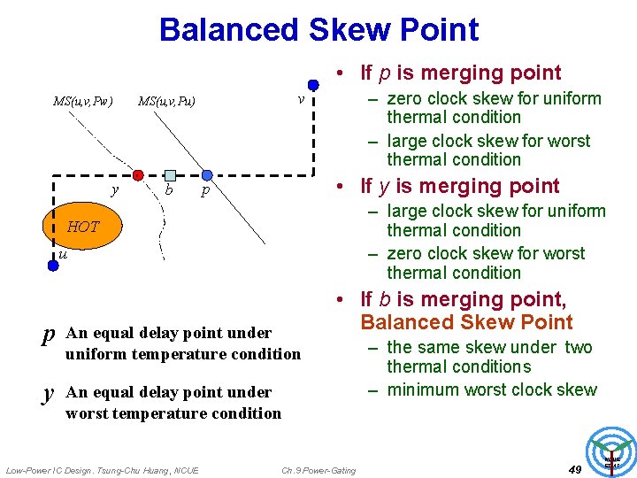
Balanced Skew Point • If p is merging point MS(u, v, Pw) y b – zero clock skew for uniform thermal condition – large clock skew for worst thermal condition v MS(u, v, Pu) • If y is merging point p – large clock skew for uniform thermal condition – zero clock skew for worst thermal condition HOT u p An equal delay point under uniform temperature condition y An equal delay point under worst temperature condition Low-Power IC Design. Tsung-Chu Huang, NCUE • If b is merging point, Balanced Skew Point Ch. 9 Power-Gating – the same skew under two thermal conditions – minimum worst clock skew 49 NCUE EDAT
![DualSpeed LFSR 3 They separate the LFSRlike RTPG into a slower part S Dual-Speed LFSR [3] • They separate the LFSR-like RTPG into a slower part S](https://slidetodoc.com/presentation_image_h/131b0c8764aee13533ecacf596a881a3/image-50.jpg)
Dual-Speed LFSR [3] • They separate the LFSR-like RTPG into a slower part S (MSB) and a normal part N (LSB) • The randomness is reduced. But they use a X 2 -test to show that the agreement of the distribution is close to the standard RTPG. [3] S. Wang and S. K. Gupta. DS-LFSR: A New BIST TPG for Low Heat Dissipation. Proc. ITC’ 97, pp. 848 -857, 1997. Low-Power IC Design. Tsung-Chu Huang, NCUE Ch. 9 Power-Gating 50 NCUE EDAT
![LowTransition RTPG 4 Assume the LFSR can generate 2 r patterns including 0 Low-Transition RTPG [4] • Assume the LFSR can generate 2 r patterns including 0](https://slidetodoc.com/presentation_image_h/131b0c8764aee13533ecacf596a881a3/image-51.jpg)
Low-Transition RTPG [4] • Assume the LFSR can generate 2 r patterns including 0 • #tran(LFSR)= 2 (r-1) • #tran(LT-RTPG) is reduced to 2 (r-k) • k=2, 3 is recommended. • 2 k tap configurations, e. g. , ( ). [4] S. Wang and S. K. Gupta. LT-RTPG: A New Test-Per-Scan BIST TPG for Low Heat Dissipation. Proc. ITC’ 99, pp. 85 -94, 1999. Low-Power IC Design. Tsung-Chu Huang, NCUE Ch. 9 Power-Gating 51 NCUE EDAT
![Analyses 4 They analyze the probability of a consecutive pattern segment for k2 Analyses [4] • They analyze the probability of a consecutive pattern segment for k=2](https://slidetodoc.com/presentation_image_h/131b0c8764aee13533ecacf596a881a3/image-52.jpg)
Analyses [4] • They analyze the probability of a consecutive pattern segment for k=2 and 3. • The input sequence of T-FF should be (110 z 11). • p(z=0)=p(z=1)=0, so it cannot generate pattern segments, 010, 101, 0110 and 1001, which are called forbidden patterns. • Example, z=4 0 1 1 100001 (110411) T 0 1 1 1 0 ? ? • Fault coverage is decreased. Low-Power IC Design. Tsung-Chu Huang, NCUE Ch. 9 Power-Gating 52 NCUE EDAT
![Properties of LTLFSR 4 Assigning identical values to neighboring inputs may decrease fault Properties of LT-LFSR [4] • Assigning identical values to neighboring inputs may decrease fault](https://slidetodoc.com/presentation_image_h/131b0c8764aee13533ecacf596a881a3/image-53.jpg)
Properties of LT-LFSR [4] • Assigning identical values to neighboring inputs may decrease fault coverage. • To make every possible pattern with equal probability, the toggle probability of any two inputs should be 0. 5 • They use the toggle probability of any two inputs to represent the randomness. • They prove that LT-RTPG can generate all patterns for enough r for some tap configuration. Low-Power IC Design. Tsung-Chu Huang, NCUE Ch. 9 Power-Gating 53 NCUE EDAT
![Experimental Results4 Results for k2 3 are listed 1435 2359 transition reductions are Experimental Results[4] • Results for k=2 (3) are listed, 14~35% (23~59%) transition reductions are](https://slidetodoc.com/presentation_image_h/131b0c8764aee13533ecacf596a881a3/image-54.jpg)
Experimental Results[4] • Results for k=2 (3) are listed, 14~35% (23~59%) transition reductions are achieved. • The fault coverage is decreased. • Their future work: latch ordering to minimize faultcoverage impact. 14~35% Low-Power IC Design. Tsung-Chu Huang, NCUE Ch. 9 Power-Gating 23~59% 54 NCUE EDAT

Data Gating Low-Power IC Design. Tsung-Chu Huang, NCUE Ch. 9 Power-Gating 55 NCUE EDAT

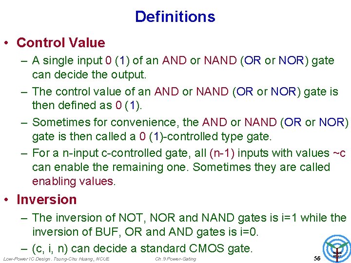
Definitions • Control Value – A single input 0 (1) of an AND or NAND (OR or NOR) gate can decide the output. – The control value of an AND or NAND (OR or NOR) gate is then defined as 0 (1). – Sometimes for convenience, the AND or NAND (OR or NOR) gate is then called a 0 (1)-controlled type gate. – For a n-input c-controlled gate, all (n-1) inputs with values ~c can enable the remaining one. Sometimes they are called enabling values. • Inversion – The inversion of NOT, NOR and NAND gates is i=1 while the inversion of BUF, OR and AND gates is i=0. – (c, i, n) can decide a standard CMOS gate. Low-Power IC Design. Tsung-Chu Huang, NCUE Ch. 9 Power-Gating 56 NCUE EDAT

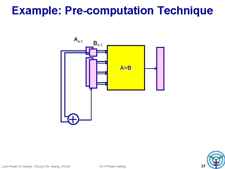
Example: Pre-computation Technique An-1 Bn-1 A>B Low-Power IC Design. Tsung-Chu Huang, NCUE Ch. 9 Power-Gating 57 NCUE EDAT

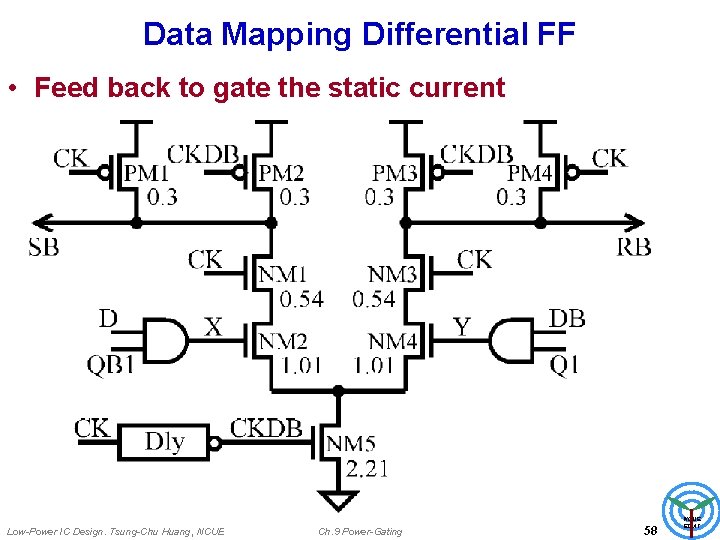
Data Mapping Differential FF • Feed back to gate the static current Low-Power IC Design. Tsung-Chu Huang, NCUE Ch. 9 Power-Gating 58 NCUE EDAT

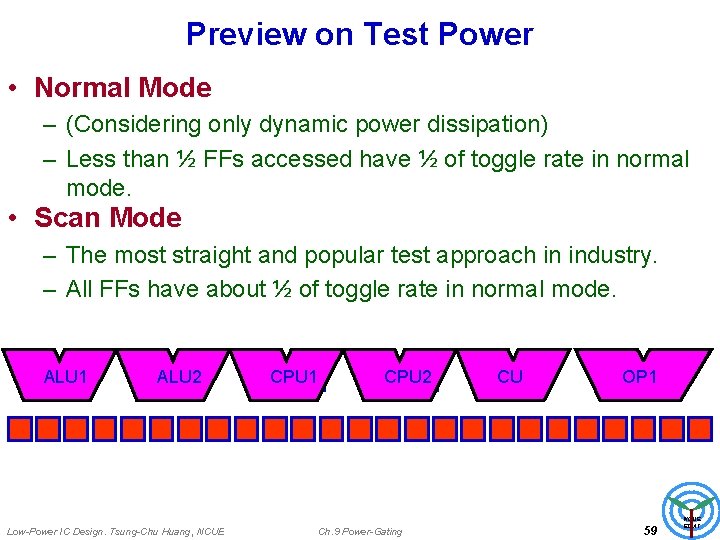
Preview on Test Power • Normal Mode – (Considering only dynamic power dissipation) – Less than ½ FFs accessed have ½ of toggle rate in normal mode. • Scan Mode – The most straight and popular test approach in industry. – All FFs have about ½ of toggle rate in normal mode. ALU 1 ALU 2 Low-Power IC Design. Tsung-Chu Huang, NCUE CPU 1 CPU 2 Ch. 9 Power-Gating CU OP 1 59 NCUE EDAT

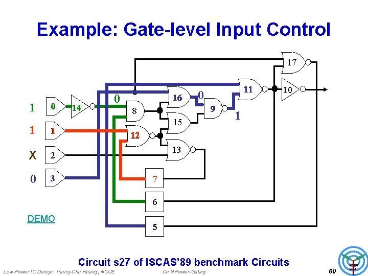
Example: Gate-level Input Control 17 1 0 1 1 X 2 0 3 14 0 16 11 0 9 8 15 10 1 12 13 7 6 DEMO 5 Circuit s 27 of ISCAS’ 89 benchmark Circuits Low-Power IC Design. Tsung-Chu Huang, NCUE Ch. 9 Power-Gating 60 NCUE EDAT

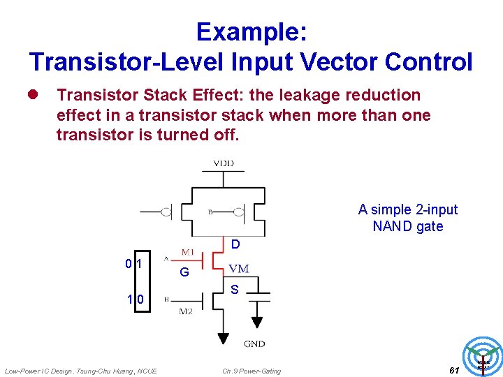
Example: Transistor-Level Input Vector Control l Transistor Stack Effect: the leakage reduction effect in a transistor stack when more than one transistor is turned off. A simple 2 -input NAND gate D 01 10 Low-Power IC Design. Tsung-Chu Huang, NCUE G S Ch. 9 Power-Gating 61 NCUE EDAT

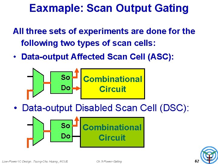
Eaxmaple: Scan Output Gating All three sets of experiments are done for the following two types of scan cells: • Data-output Affected Scan Cell (ASC): So Do Combinational Data output are affected during scan. Circuit • Data-output Disabled Scan Cell (DSC): So Do Low-Power IC Design. Tsung-Chu Huang, NCUE Combinational Data output are disabled during scan. Circuit Ch. 9 Power-Gating 62 NCUE EDAT
![Switching Activity Masking Technique1 Using a NOR NAND to mask Q by Switching Activity Masking Technique[1] • • Using a NOR (NAND) to mask Q by](https://slidetodoc.com/presentation_image_h/131b0c8764aee13533ecacf596a881a3/image-63.jpg)
Switching Activity Masking Technique[1] • • Using a NOR (NAND) to mask Q by TEST (NORMAL) = DSC (Disabled Scan Cell) Overhead: 1 NOR/Cell, about 20%/cell, but few /CUT. Performance impact: < 10% (delay) NOR [1] S. Gerstendorfer and H. -J. Wunderlich. Minimized Power Consumption for Scan-based BIST. Proc. ITC’ 99, pp. 77 -84, 1999. Low-Power IC Design. Tsung-Chu Huang, NCUE Ch. 9 Power-Gating 63 NCUE EDAT

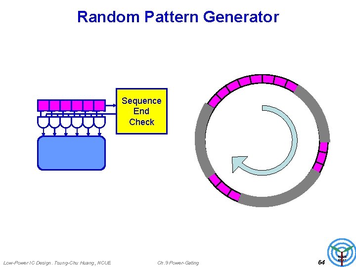
Random Pattern Generator Sequence End Check Low-Power IC Design. Tsung-Chu Huang, NCUE Ch. 9 Power-Gating 64 NCUE EDAT
![Decoding Exhaustive Patterns as TPG1 Deterministic patterns are selected by a PLAlike decoder Decoding Exhaustive Patterns as TPG[1] • Deterministic patterns are selected by a PLA-like decoder](https://slidetodoc.com/presentation_image_h/131b0c8764aee13533ecacf596a881a3/image-65.jpg)
Decoding Exhaustive Patterns as TPG[1] • Deterministic patterns are selected by a PLA-like decoder from a counter. Low-Power IC Design. Tsung-Chu Huang, NCUE Ch. 9 Power-Gating 65 NCUE EDAT
![PeakPower Reduction by Partitioning 2 Basic Concept The transversals of justification and propagation Peak-Power Reduction by Partitioning [2] • Basic Concept: The transversals of justification and propagation](https://slidetodoc.com/presentation_image_h/131b0c8764aee13533ecacf596a881a3/image-66.jpg)
Peak-Power Reduction by Partitioning [2] • Basic Concept: The transversals of justification and propagation are just a part of the CUT but the affected area is usually larger. • Example: circuit c 17 A F B C D I Hi H Hj J G K L E [2] P. Girard, L. Guiller, C. Landrault, and S. Pravossoudovitch. Circuit Partitioning for Low Power BIST Design with Minimized Peak Power Consumption. Proc. ATS’ 99, pp. 89 -94, 1999. Low-Power IC Design. Tsung-Chu Huang, NCUE Ch. 9 Power-Gating 66 NCUE EDAT
![Partitioning by MuxDe Mux Inserting2 The boundary wires are separated by inserting multiplexers Partitioning by Mux/De. Mux Inserting[2] • The boundary wires are separated by inserting multiplexers](https://slidetodoc.com/presentation_image_h/131b0c8764aee13533ecacf596a881a3/image-67.jpg)
Partitioning by Mux/De. Mux Inserting[2] • The boundary wires are separated by inserting multiplexers and de-multiplexers. • Control signal: #states = #part + 1 Low-Power IC Design. Tsung-Chu Huang, NCUE Ch. 9 Power-Gating 67 NCUE EDAT
![Multilevel Graph Bisection Algorithm2 Coarsening because some nodes cannot be separated e g Multilevel Graph Bisection Algorithm[2] • Coarsening because some nodes cannot be separated, e. g.](https://slidetodoc.com/presentation_image_h/131b0c8764aee13533ecacf596a881a3/image-68.jpg)
Multilevel Graph Bisection Algorithm[2] • Coarsening because some nodes cannot be separated, e. g. , XOR, Latch, FF, cliques, e. t. c. • Partitioning criteria: and mincut Coarsening Uncoarsening Partitioning Low-Power IC Design. Tsung-Chu Huang, NCUE Ch. 9 Power-Gating 68 NCUE EDAT
![Experimental Results2 and Comments Average Reduction Percentages of 14 Circuits Peak Experimental Results[2] and Comments • Average Reduction Percentages of 14 Circuits: – – Peak](https://slidetodoc.com/presentation_image_h/131b0c8764aee13533ecacf596a881a3/image-69.jpg)
Experimental Results[2] and Comments • Average Reduction Percentages of 14 Circuits: – – Peak Power: 35% Average Power: 50% Total Energy: 60% Application Time: 20% longer. • Impacts: – Fault Coverage: a little improved. – Area Overhead: 1. 5~22% – Performance: No, because critical-path cuts are forbidden. • Comments: – The basic concepts for other purposes have been proposed, e. g. , partitioning for pseudo-exhaustive test, partitioning for broadcasting, and those in Weste’s textbook. Low-Power IC Design. Tsung-Chu Huang, NCUE Ch. 9 Power-Gating 69 NCUE EDAT

Power Gating (Supply Gating) Low-Power IC Design. Tsung-Chu Huang, NCUE Ch. 9 Power-Gating 70 NCUE EDAT

Outline • • Dynamic Power Management Power Grid & Leakage and Model Power Concept Classification – Switch Retention, Granularity, Distribution, Mode • CCS Sizing and Impacts • TSMC RDF 6 & RDF 7 on Power-Gating • Power-Gating Impact Reduction Techniques Low-Power IC Design. Tsung-Chu Huang, NCUE Ch. 9 Power-Gating 71 NCUE EDAT

Power Gating Concept Low-Power IC Design. Tsung-Chu Huang, NCUE Ch. 9 Power-Gating 72 NCUE EDAT

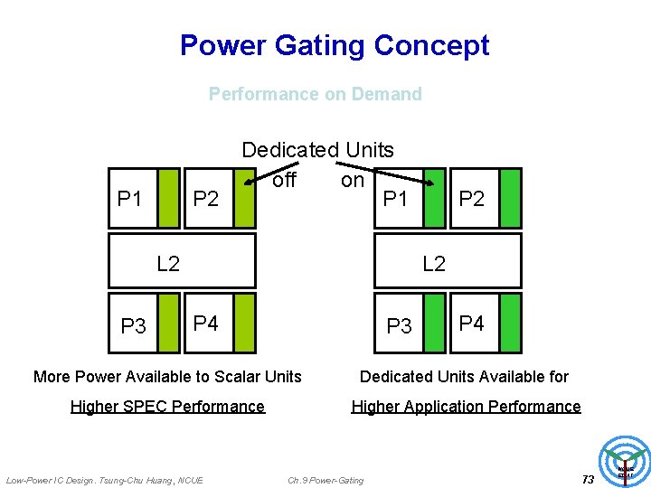
Power Gating Concept Performance on Demand P 1 P 2 Dedicated Units off on P 1 L 2 P 3 P 2 L 2 P 4 P 3 P 4 More Power Available to Scalar Units Dedicated Units Available for Higher SPEC Performance Higher Application Performance Low-Power IC Design. Tsung-Chu Huang, NCUE Ch. 9 Power-Gating 73 NCUE EDAT

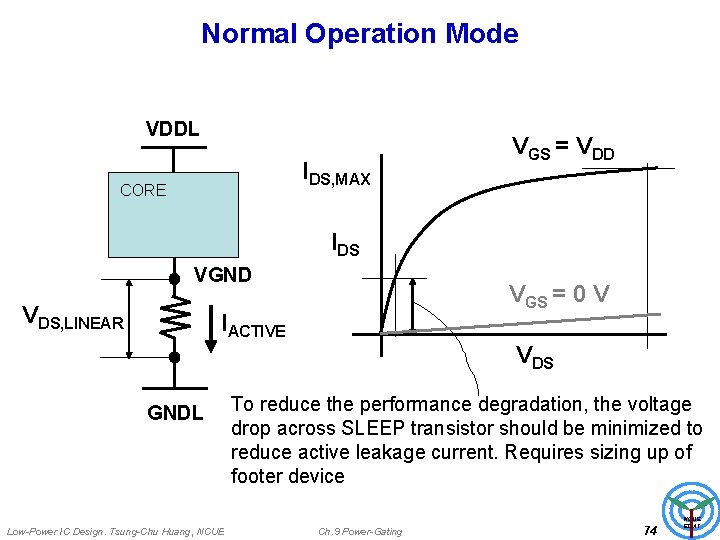
Normal Operation Mode VDDL IDS, MAX CORE VGS = VDD IDS VGND VDS, LINEAR VGS = 0 V IACTIVE VDS GNDL Low-Power IC Design. Tsung-Chu Huang, NCUE To reduce the performance degradation, the voltage drop across SLEEP transistor should be minimized to reduce active leakage current. Requires sizing up of footer device Ch. 9 Power-Gating 74 NCUE EDAT

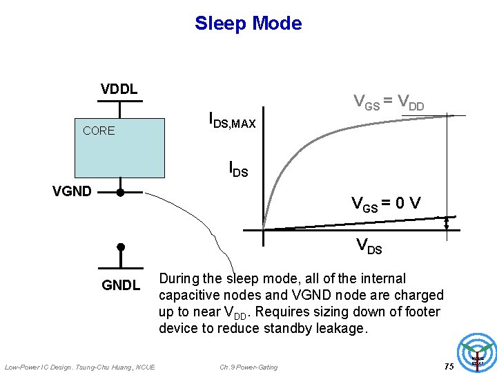
Sleep Mode VDDL CORE IDS, MAX VGS = VDD IDS VGND VGS = 0 V VDS GNDL Low-Power IC Design. Tsung-Chu Huang, NCUE During the sleep mode, all of the internal capacitive nodes and VGND node are charged up to near VDD. Requires sizing down of footer device to reduce standby leakage. Ch. 9 Power-Gating 75 NCUE EDAT

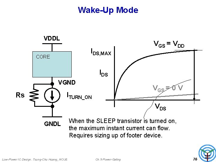
Wake-Up Mode VDDL IDS, MAX CORE VGS = VDD IDS VGND VGS = 0 V ITURN_ON Rs VDS GNDL Low-Power IC Design. Tsung-Chu Huang, NCUE When the SLEEP transistor is turned on, the maximum instant current can flow. Requires sizing up of footer device. Ch. 9 Power-Gating 76 NCUE EDAT

Current Cutoff Switch Classification Low-Power IC Design. Tsung-Chu Huang, NCUE Ch. 9 Power-Gating 77 NCUE EDAT

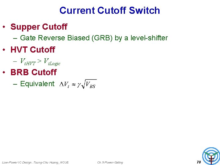
Current Cutoff Switch • Supper Cutoff – Gate Reverse Biased (GRB) by a level-shifter • HVT Cutoff – Vt. HVT > Vt. Logic • BRB Cutoff – Equivalent Low-Power IC Design. Tsung-Chu Huang, NCUE Ch. 9 Power-Gating 78 NCUE EDAT

Power Management Low-Power IC Design. Tsung-Chu Huang, NCUE Ch. 9 Power-Gating 79 NCUE EDAT

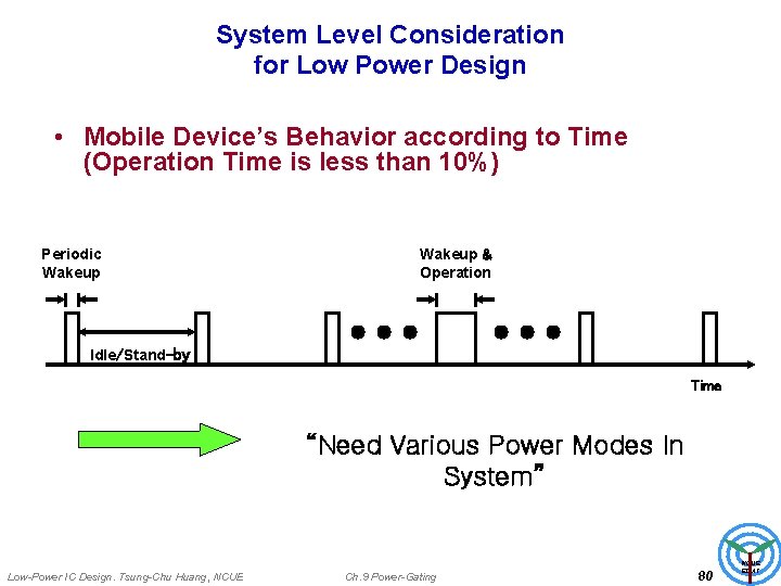
System Level Consideration for Low Power Design • Mobile Device’s Behavior according to Time (Operation Time is less than 10%) Periodic Wakeup & Operation Idle/Stand-by Time “Need Various Power Modes In System” Low-Power IC Design. Tsung-Chu Huang, NCUE Ch. 9 Power-Gating 80 NCUE EDAT

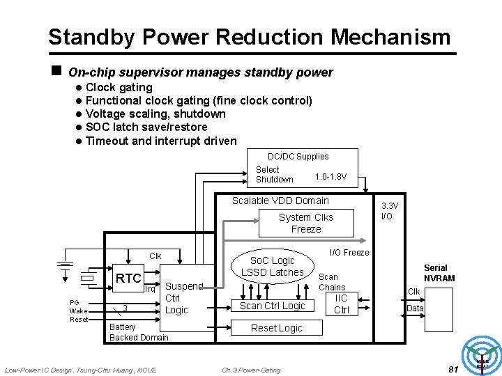
Standby Power Reduction Mechanism n On-chip supervisor manages standby power l l l Clock gating Functional clock gating (fine clock control) Voltage scaling, shutdown SOC latch save/restore Timeout and interrupt driven DC/DC Supplies Select Shutdown 1. 0 -1. 8 V Scalable VDD Domain 3. 3 V I/O System Clks Freeze Clk RTC PG Wake Reset Irq 3 So. C Logic LSSD Latches Suspend Ctrl Logic Battery Backed Domain Low-Power IC Design. Tsung-Chu Huang, NCUE Scan Ctrl Logic I/O Freeze Scan Chains IIC Ctrl Serial NVRAM Clk Data Reset Logic Ch. 9 Power-Gating 81 NCUE EDAT

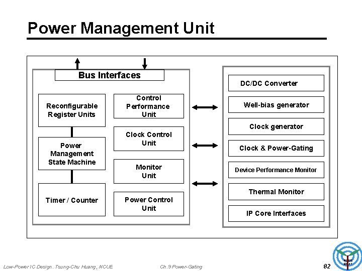
Power Management Unit Bus Interfaces Reconfigurable Register Units DC/DC Converter Control Performance Unit Well-bias generator Clock generator Power Management State Machine Clock Control Unit Monitor Unit Clock & Power-Gating Device Performance Monitor Thermal Monitor Timer / Counter Low-Power IC Design. Tsung-Chu Huang, NCUE Power Control Unit Ch. 9 Power-Gating IP Core Interfaces 82 NCUE EDAT

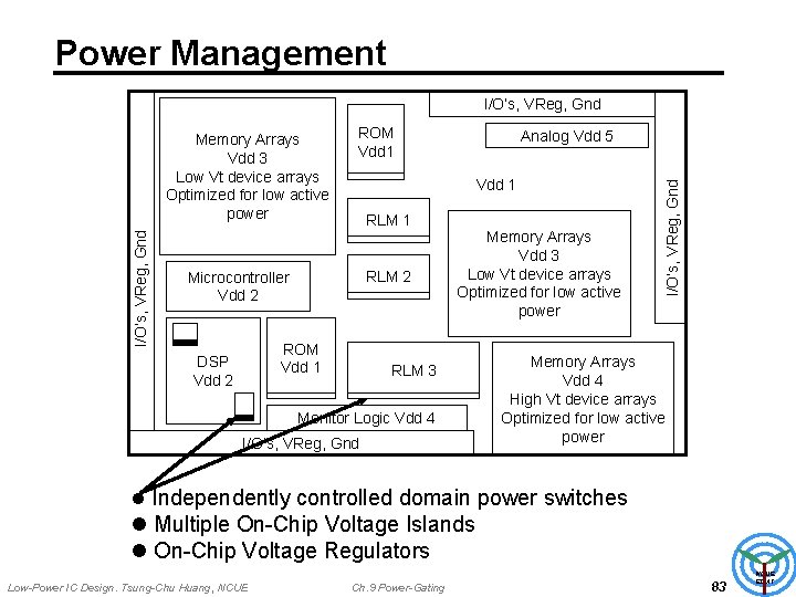
Power Management I/O’s, VReg, Gnd ROM Vdd 1 RLM 2 Microcontroller Vdd 2 ROM Vdd 1 DSP Vdd 2 Analog Vdd 5 Memory Arrays Vdd 3 Low Vt device arrays Optimized for low active power RLM 3 Monitor Logic Vdd 4 I/O’s, VReg, Gnd Memory Arrays Vdd 3 Low Vt device arrays Optimized for low active power Memory Arrays Vdd 4 High Vt device arrays Optimized for low active power l Independently controlled domain power switches l Multiple On-Chip Voltage Islands l On-Chip Voltage Regulators Low-Power IC Design. Tsung-Chu Huang, NCUE Ch. 9 Power-Gating 83 NCUE EDAT

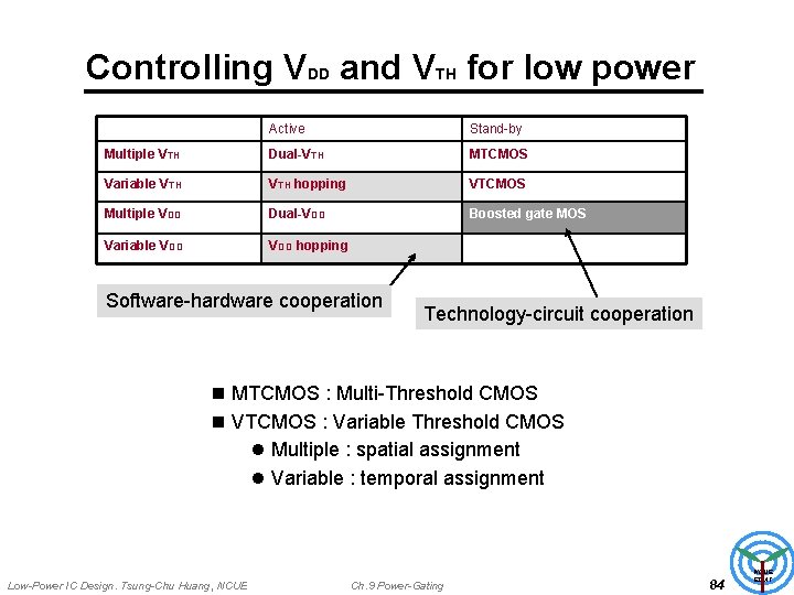
Controlling VDD and VTH for low power Active Stand-by Multiple VTH Dual-VTH MTCMOS Variable VTH hopping VTCMOS Multiple VDD Dual-VDD Boosted gate MOS Variable VDD hopping Software-hardware cooperation Technology-circuit cooperation n MTCMOS : Multi-Threshold CMOS n VTCMOS : Variable Threshold CMOS l Multiple : spatial assignment l Variable : temporal assignment Low-Power IC Design. Tsung-Chu Huang, NCUE Ch. 9 Power-Gating 84 NCUE EDAT

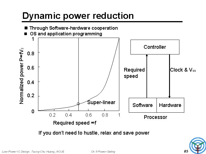
Dynamic power reduction n Through Software-hardware cooperation n OS and application programming Normalized power P∞f. V 2 1 Controller 0. 8 0. 6 Clock & VDD Required speed 0. 4 0. 2 Super-linear 0 0. 2 0. 4 0. 6 0. 8 Software 1 Hardware Processor Required speed ∞f If you don’t need to hustle, relax and save power Low-Power IC Design. Tsung-Chu Huang, NCUE Ch. 9 Power-Gating 85 NCUE EDAT

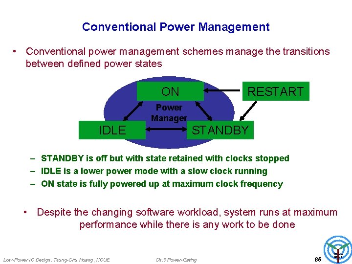
Conventional Power Management • Conventional power management schemes manage the transitions between defined power states ON RESTART Power Manager IDLE STANDBY – STANDBY is off but with state retained with clocks stopped – IDLE is a lower power mode with a slow clock running – ON state is fully powered up at maximum clock frequency • Despite the changing software workload, system runs at maximum performance while there is any work to be done Low-Power IC Design. Tsung-Chu Huang, NCUE Ch. 9 Power-Gating 86 NCUE EDAT

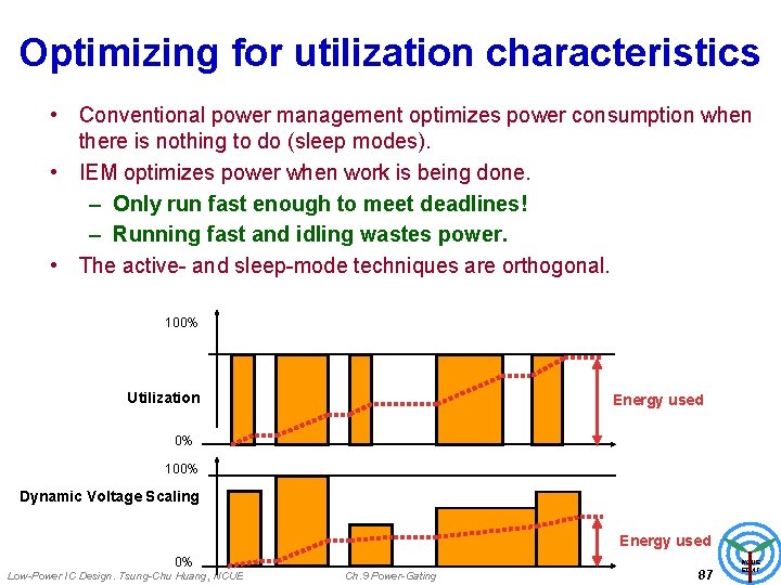
Optimizing for utilization characteristics • Conventional power management optimizes power consumption when there is nothing to do (sleep modes). • IEM optimizes power when work is being done. – Only run fast enough to meet deadlines! – Running fast and idling wastes power. • The active- and sleep-mode techniques are orthogonal. 100% Utilization Energy used 0% 100% Dynamic Voltage Scaling Energy used 0% Low-Power IC Design. Tsung-Chu Huang, NCUE Ch. 9 Power-Gating 87 NCUE EDAT

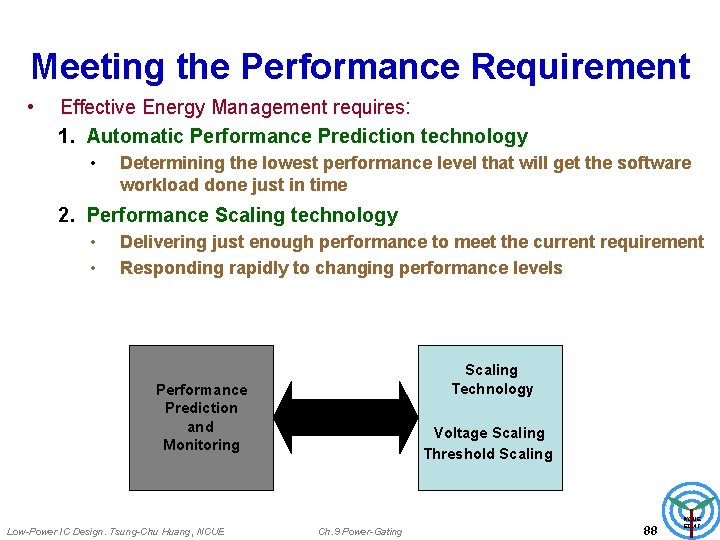
Meeting the Performance Requirement • Effective Energy Management requires: 1. Automatic Performance Prediction technology • Determining the lowest performance level that will get the software workload done just in time 2. Performance Scaling technology • • Delivering just enough performance to meet the current requirement Responding rapidly to changing performance levels Scaling Technology Performance Prediction and Monitoring Low-Power IC Design. Tsung-Chu Huang, NCUE Voltage Scaling Threshold Scaling Ch. 9 Power-Gating 88 NCUE EDAT

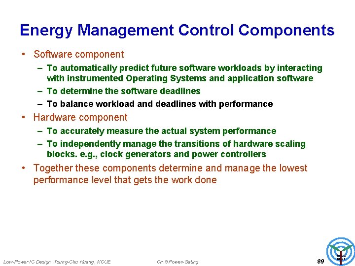
Energy Management Control Components • Software component – To automatically predict future software workloads by interacting with instrumented Operating Systems and application software – To determine the software deadlines – To balance workload and deadlines with performance • Hardware component – To accurately measure the actual system performance – To independently manage the transitions of hardware scaling blocks. e. g. , clock generators and power controllers • Together these components determine and manage the lowest performance level that gets the work done Low-Power IC Design. Tsung-Chu Huang, NCUE Ch. 9 Power-Gating 89 NCUE EDAT

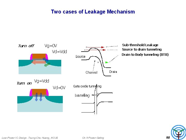
Two cases of Leakage Mechanism Turn off Turn on Vg=0 V Vd=Vdd Sub-threshold Leakage Source to drain tunneling Drain to Body tunneling (BTB) Vg=Vdd Vd=0 V Low-Power IC Design. Tsung-Chu Huang, NCUE Gate oxide tunneling Ch. 9 Power-Gating 90 NCUE EDAT

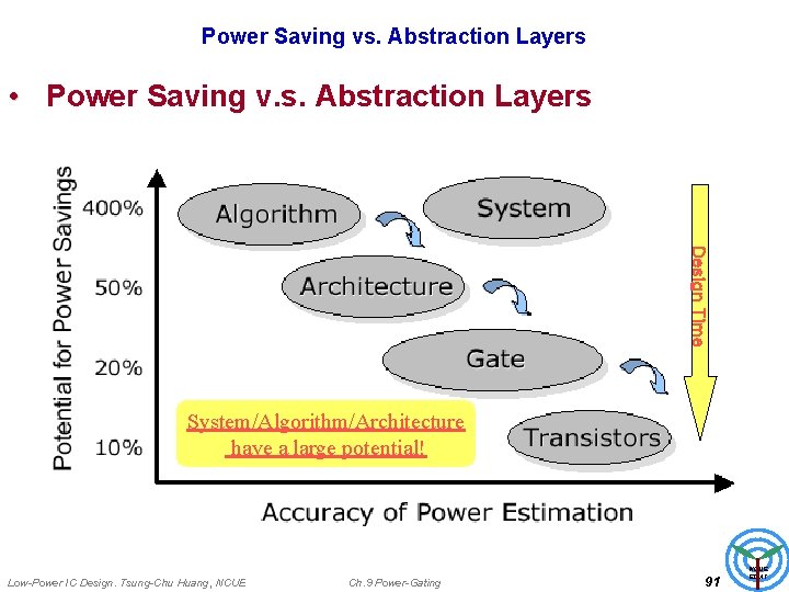
Power Saving vs. Abstraction Layers • Power Saving v. s. Abstraction Layers Design Time System/Algorithm/Architecture have a large potential! Low-Power IC Design. Tsung-Chu Huang, NCUE Ch. 9 Power-Gating 91 NCUE EDAT

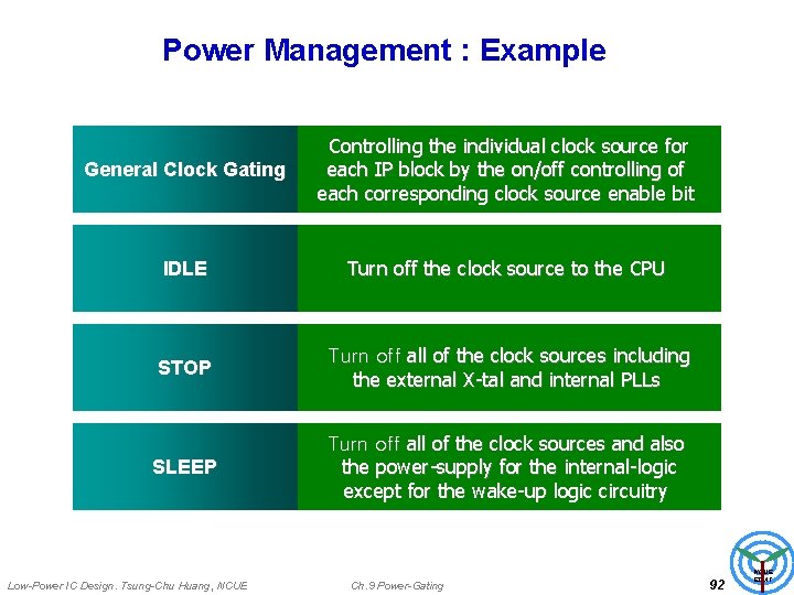
Power Management : Example General Clock Gating Controlling the individual clock source for each IP block by the on/off controlling of each corresponding clock source enable bit IDLE Turn off the clock source to the CPU STOP Turn off all of the clock sources including the external X-tal and internal PLLs SLEEP Turn off all of the clock sources and also the power-supply for the internal-logic except for the wake-up logic circuitry Low-Power IC Design. Tsung-Chu Huang, NCUE Ch. 9 Power-Gating 92 NCUE EDAT

Leakages Low-Power IC Design. Tsung-Chu Huang, NCUE Ch. 9 Power-Gating 93 NCUE EDAT

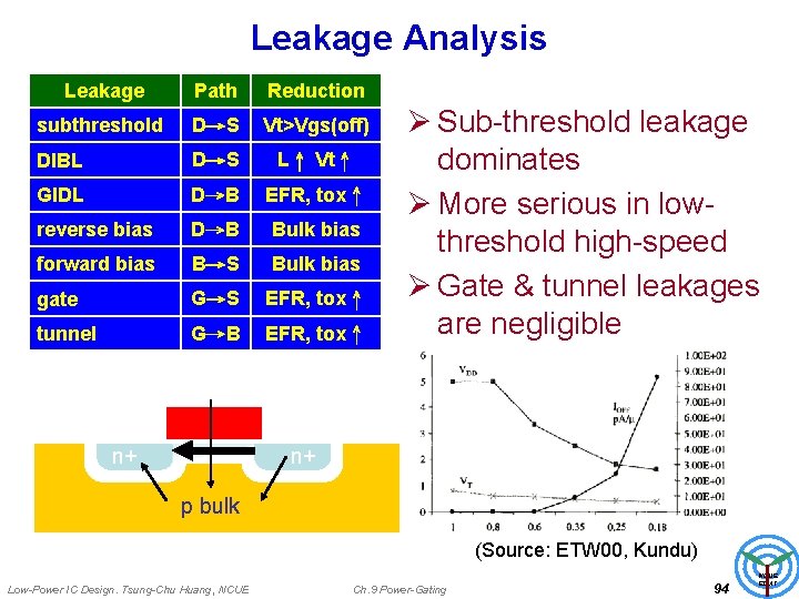
Leakage Analysis Leakage Path Reduction subthreshold D→S Vt>Vgs(off) DIBL D→S L↑ Vt↑ GIDL D→B EFR, tox↑ reverse bias D→B Bulk bias forward bias B→S Bulk bias gate G→S EFR, tox↑ tunnel G→B EFR, tox↑ Ø Sub-threshold leakage dominates Ø More serious in lowthreshold high-speed Ø Gate & tunnel leakages are negligible gate source drain n+ n+ p bulk (Source: ETW 00, Kundu) Low-Power IC Design. Tsung-Chu Huang, NCUE Ch. 9 Power-Gating 94 NCUE EDAT

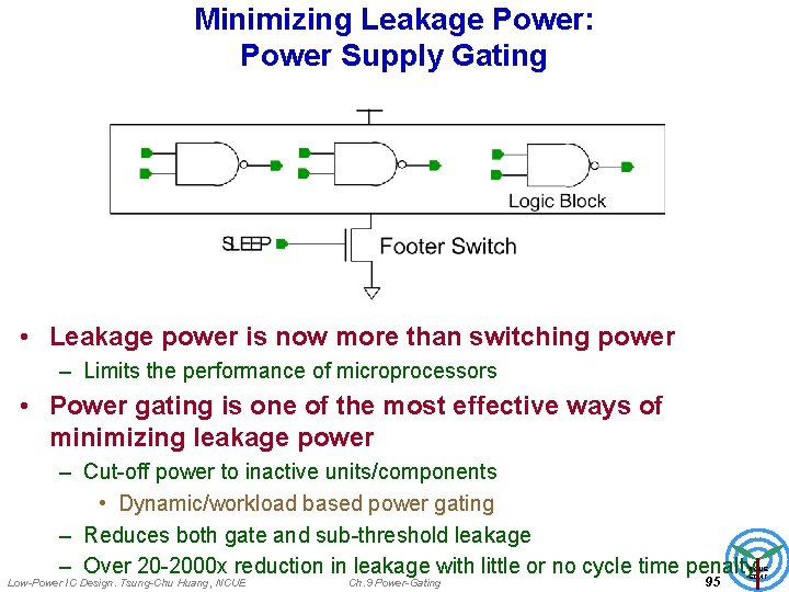
Minimizing Leakage Power: Power Supply Gating • Leakage power is now more than switching power – Limits the performance of microprocessors • Power gating is one of the most effective ways of minimizing leakage power – Cut-off power to inactive units/components • Dynamic/workload based power gating – Reduces both gate and sub-threshold leakage – Over 20 -2000 x reduction in leakage with little or no cycle time penalty. Low-Power IC Design. Tsung-Chu Huang, NCUE Ch. 9 Power-Gating 95 NCUE EDAT

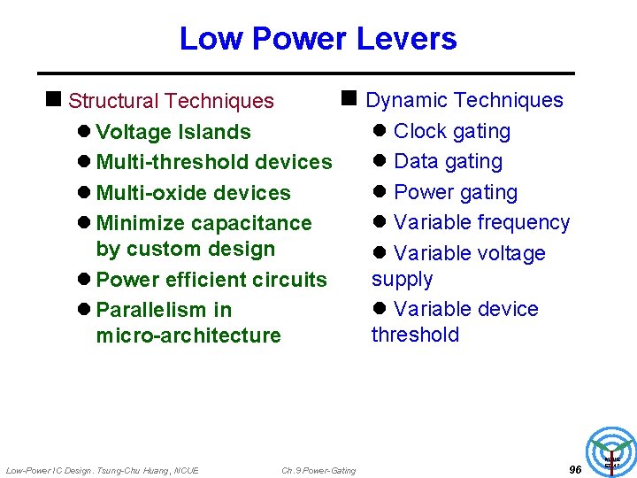
Low Power Levers n Dynamic Techniques n Structural Techniques l Voltage Islands l Multi-threshold devices l Multi-oxide devices l Minimize capacitance by custom design l Power efficient circuits l Parallelism in micro-architecture Low-Power IC Design. Tsung-Chu Huang, NCUE Ch. 9 Power-Gating l Clock gating l Data gating l Power gating l Variable frequency l Variable voltage supply l Variable device threshold 96 NCUE EDAT

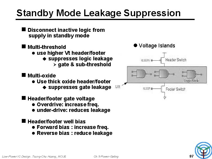
Standby Mode Leakage Suppression n Disconnect inactive logic from supply in standby mode l Voltage Islands n Multi-threshold l use higher Vt header/footer u suppresses logic leakage Ø gate & sub-threshold n Multi-oxide l Use thick oxide header/footer u suppresses gate leakage n Header/footer gate voltage l l Overdrive: increase freq. under-drive: reduces leakage n Header/footer well bias l l Forward bias : increase freq. Reverse bias : reduce leakage Low-Power IC Design. Tsung-Chu Huang, NCUE Ch. 9 Power-Gating 97 NCUE EDAT

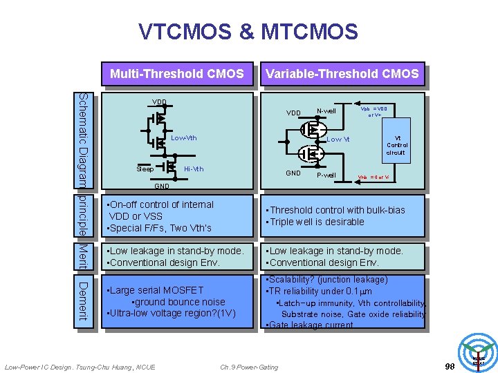
VTCMOS & MTCMOS Multi-Threshold CMOS Variable-Threshold CMOS Schematic Diagram principle Merit VDD Low-Vth Sleep N-well Low Vt Hi-Vth GND P-well Vpb = VDD or V+ Vt Control circuit Vnb = 0 or V- GND • On-off control of internal VDD or VSS • Special F/Fs, Two Vth’s • Threshold control with bulk-bias • Triple well is desirable • Low leakage in stand-by mode. • Conventional design Env. Demerit • Large serial MOSFET • ground bounce noise • Ultra-low voltage region? (1 V) Low-Power IC Design. Tsung-Chu Huang, NCUE • Scalability? (junction leakage) • TR reliability under 0. 1 mm • Latch-up immunity, Vth controllability, Substrate noise, Gate oxide reliability • Gate leakage current Ch. 9 Power-Gating 98 NCUE EDAT

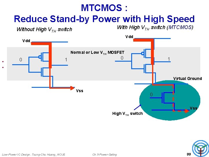
MTCMOS : Reduce Stand-by Power with High Speed With High VTH switch (MTCMOS) Without High VTH switch Vdd Normal or Low VTH MOSFET • • 0 1 1 With 0 High VTH switch, much lower leakage current flows between Vdd and Vss High VTH MOSFET should have much lower ( >10 X) leakage current compared to normal VTH MOSFET Virtual Ground Vss 0 Vss High VTH switch Low-Power IC Design. Tsung-Chu Huang, NCUE Ch. 9 Power-Gating 99 NCUE EDAT

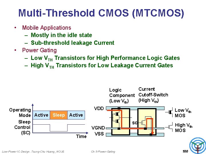
Multi-Threshold CMOS (MTCMOS) • Mobile Applications – Mostly in the idle state – Sub-threshold leakage Current • Power Gating – Low VTH Transistors for High Performance Logic Gates – High VTH Transistors for Low Leakage Current Gates Current Logic Component Cutoff-Switch (High Vth) (Low Vth) Operating Mode Active Sleep Control (SC) Time Low-Power IC Design. Tsung-Chu Huang, NCUE VDD Low Vth MOS SC VGND VSS Ch. 9 Power-Gating High Vth MOS 100 NCUE EDAT

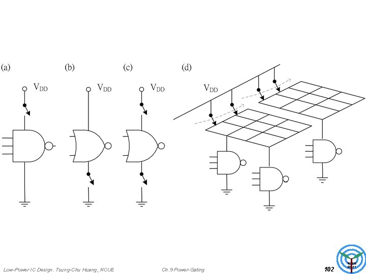
Power-Grid and Sub-Power-Grid Low-Power IC Design. Tsung-Chu Huang, NCUE Ch. 9 Power-Gating 101 NCUE EDAT

Low-Power IC Design. Tsung-Chu Huang, NCUE Ch. 9 Power-Gating 102 NCUE EDAT

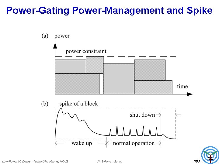
Power-Gating Power-Management and Spike Low-Power IC Design. Tsung-Chu Huang, NCUE Ch. 9 Power-Gating 103 NCUE EDAT

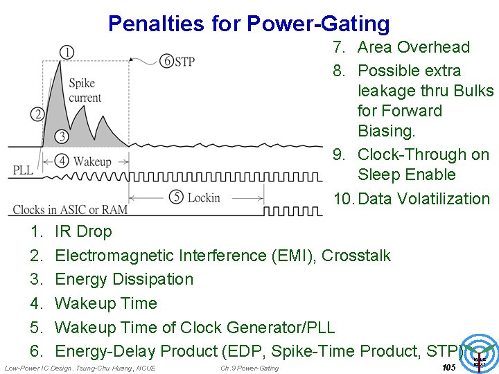
Power-Gating Impact/Penalty Low-Power IC Design. Tsung-Chu Huang, NCUE Ch. 9 Power-Gating 104 NCUE EDAT

Penalties for Power-Gating 7. Area Overhead 8. Possible extra leakage thru Bulks for Forward Biasing. 9. Clock-Through on Sleep Enable 10. Data Volatilization 1. 2. 3. 4. 5. 6. IR Drop Electromagnetic Interference (EMI), Crosstalk Energy Dissipation Wakeup Time of Clock Generator/PLL Energy-Delay Product (EDP, Spike-Time Product, STP) Low-Power IC Design. Tsung-Chu Huang, NCUE Ch. 9 Power-Gating 105 NCUE EDAT

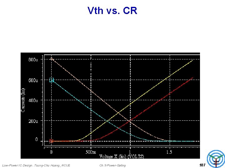
Current-Ratio Model Low-Power IC Design. Tsung-Chu Huang, NCUE Ch. 9 Power-Gating 106 NCUE EDAT

Vth vs. CR Low-Power IC Design. Tsung-Chu Huang, NCUE Ch. 9 Power-Gating 107 NCUE EDAT
![OnOff Current Ratio Ø IonIoff trades delay cost with leakage reduction ISCA 02 Heo On/Off Current Ratio Ø Ion/Ioff trades delay cost with leakage reduction [ISCA 02 Heo],](https://slidetodoc.com/presentation_image_h/131b0c8764aee13533ecacf596a881a3/image-108.jpg)
On/Off Current Ratio Ø Ion/Ioff trades delay cost with leakage reduction [ISCA 02 Heo], according to ITRS 2000. Low-Power IC Design. Tsung-Chu Huang, NCUE Ch. 9 Power-Gating 108 NCUE EDAT

Power-Gating Classification Low-Power IC Design. Tsung-Chu Huang, NCUE Ch. 9 Power-Gating 109 NCUE EDAT

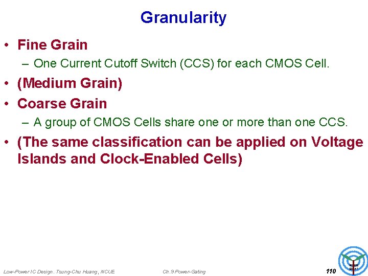
Granularity • Fine Grain – One Current Cutoff Switch (CCS) for each CMOS Cell. • (Medium Grain) • Coarse Grain – A group of CMOS Cells share one or more than one CCS. • (The same classification can be applied on Voltage Islands and Clock-Enabled Cells) Low-Power IC Design. Tsung-Chu Huang, NCUE Ch. 9 Power-Gating 110 NCUE EDAT

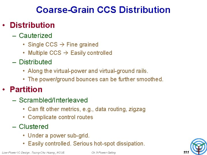
Coarse-Grain CCS Distribution • Distribution – Cauterized • Single CCS Fine grained • Multiple CCS Easily controlled – Distributed • Along the virtual-power and virtual-ground rails. • The power/ground bounces can be further smoothed. • Partition – Scrambled/Interleaved • Can fit other metrics, e. g. , data routing, zigzag • Complicate control routes – Clustered • Under a power sub-grid. • Easily controlled. Serious hot-spot dissipation. Low-Power IC Design. Tsung-Chu Huang, NCUE Ch. 9 Power-Gating 111 NCUE EDAT

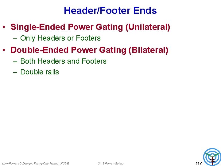
Header/Footer Ends • Single-Ended Power Gating (Unilateral) – Only Headers or Footers • Double-Ended Power Gating (Bilateral) – Both Headers and Footers – Double rails Low-Power IC Design. Tsung-Chu Huang, NCUE Ch. 9 Power-Gating 112 NCUE EDAT

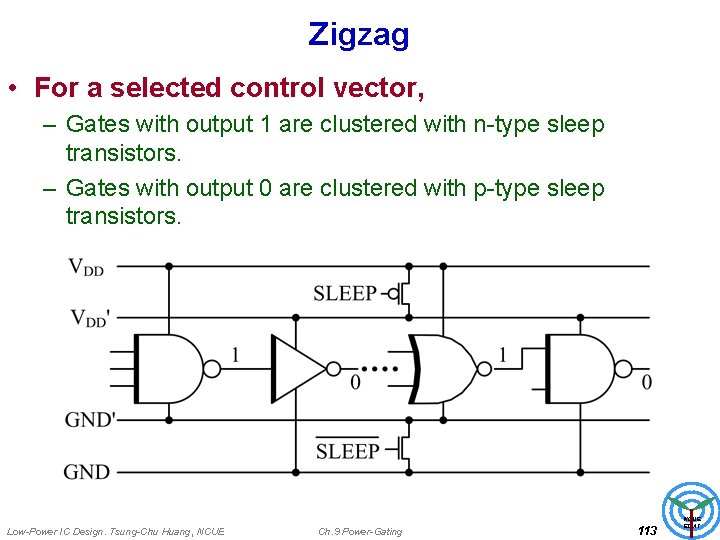
Zigzag • For a selected control vector, – Gates with output 1 are clustered with n-type sleep transistors. – Gates with output 0 are clustered with p-type sleep transistors. Low-Power IC Design. Tsung-Chu Huang, NCUE Ch. 9 Power-Gating 113 NCUE EDAT

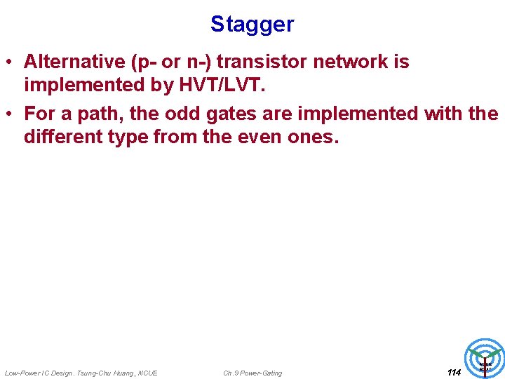
Stagger • Alternative (p- or n-) transistor network is implemented by HVT/LVT. • For a path, the odd gates are implemented with the different type from the even ones. Low-Power IC Design. Tsung-Chu Huang, NCUE Ch. 9 Power-Gating 114 NCUE EDAT

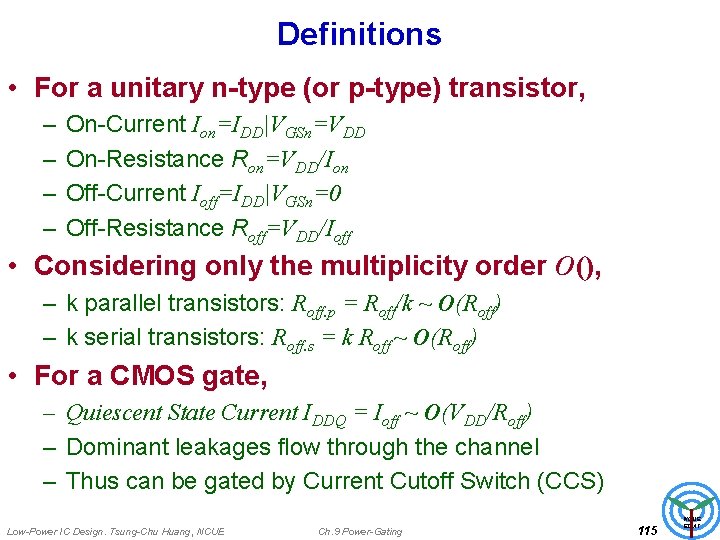
Definitions • For a unitary n-type (or p-type) transistor, – – On-Current Ion=IDD|VGSn=VDD On-Resistance Ron=VDD/Ion Off-Current Ioff=IDD|VGSn=0 Off-Resistance Roff=VDD/Ioff • Considering only the multiplicity order O(), – k parallel transistors: Roff. p = Roff/k ~ O(Roff) – k serial transistors: Roff. s = k Roff ~ O(Roff) • For a CMOS gate, – Quiescent State Current IDDQ = Ioff ~ O(VDD/Roff) – Dominant leakages flow through the channel – Thus can be gated by Current Cutoff Switch (CCS) Low-Power IC Design. Tsung-Chu Huang, NCUE Ch. 9 Power-Gating 115 NCUE EDAT

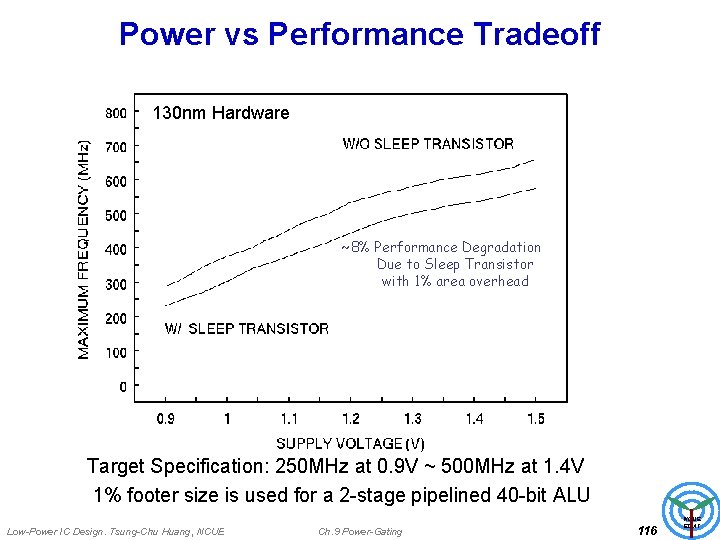
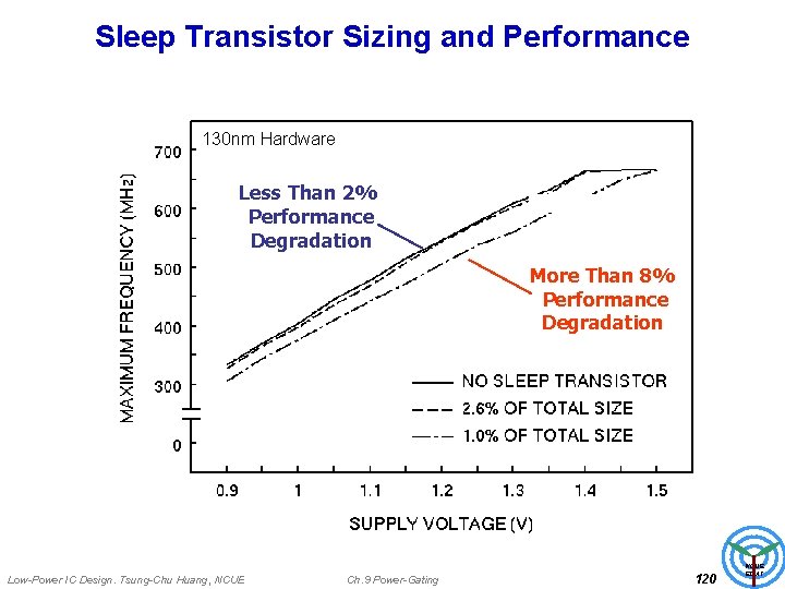
Power vs Performance Tradeoff 130 nm Hardware ~8% Performance Degradation Due to Sleep Transistor with 1% area overhead Target Specification: 250 MHz at 0. 9 V ~ 500 MHz at 1. 4 V 1% footer size is used for a 2 -stage pipelined 40 -bit ALU Low-Power IC Design. Tsung-Chu Huang, NCUE Ch. 9 Power-Gating 116 NCUE EDAT

CCS Sizing Low-Power IC Design. Tsung-Chu Huang, NCUE Ch. 9 Power-Gating 117 NCUE EDAT

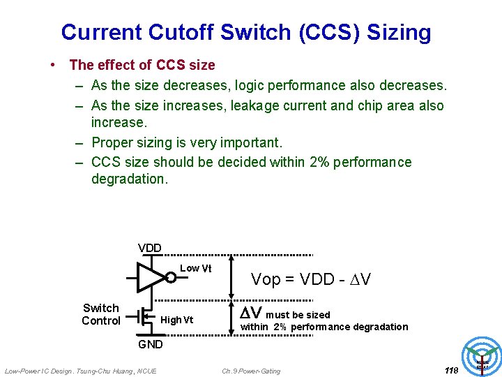
Current Cutoff Switch (CCS) Sizing • The effect of CCS size – As the size decreases, logic performance also decreases. – As the size increases, leakage current and chip area also increase. – Proper sizing is very important. – CCS size should be decided within 2% performance degradation. VDD Low Vt Switch Control High Vt Vop = VDD - V V must be sized within 2% performance degradation . GND Low-Power IC Design. Tsung-Chu Huang, NCUE Ch. 9 Power-Gating 118 NCUE EDAT

Performance Constraint Sizing • For a small performance degradation rate, r – Extra delay is about r X 100% – If delay is about proportional to (VDD-Vth)a, the voltage drop should be limited to ar. – Imax Estimation – Voltage Drop= Imax. Roff. CCS • For fine-grained power-gating, – Roff. HVT >> Roff. LVT >> Ron. HVT Ron. LVT under area compromised. – Balznced/Equal Noise Margin Design Low-Power IC Design. Tsung-Chu Huang, NCUE Ch. 9 Power-Gating 119 NCUE EDAT

Sleep Transistor Sizing and Performance 130 nm Hardware Less Than 2% Performance Degradation More Than 8% Performance Degradation Low-Power IC Design. Tsung-Chu Huang, NCUE Ch. 9 Power-Gating 120 NCUE EDAT

CCS Placement Low-Power IC Design. Tsung-Chu Huang, NCUE Ch. 9 Power-Gating 121 NCUE EDAT

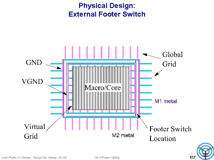
Physical Design: External Footer Switch Low-Power IC Design. Tsung-Chu Huang, NCUE Ch. 9 Power-Gating 122 NCUE EDAT

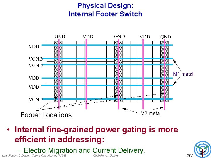
Physical Design: Internal Footer Switch • Internal fine-grained power gating is more efficient in addressing: – Electro-Migration and Current Delivery. Low-Power IC Design. Tsung-Chu Huang, NCUE Ch. 9 Power-Gating 123 NCUE EDAT

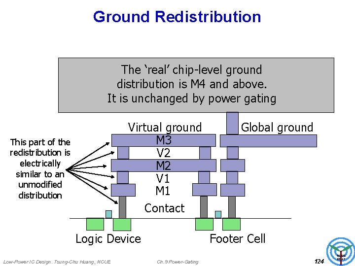
Ground Redistribution The ‘real’ chip-level ground distribution is M 4 and above. It is unchanged by power gating Virtual ground M 3 V 2 M 2 V 1 M 1 Contact This part of the redistribution is electrically similar to an unmodified distribution Logic Device Low-Power IC Design. Tsung-Chu Huang, NCUE Global ground Footer Cell Ch. 9 Power-Gating 124 NCUE EDAT

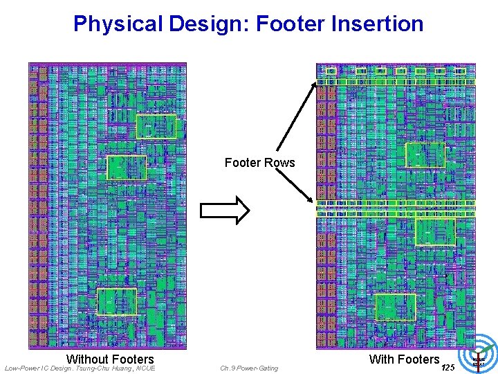
Physical Design: Footer Insertion Footer Rows Without Footers Low-Power IC Design. Tsung-Chu Huang, NCUE Ch. 9 Power-Gating With Footers 125 NCUE EDAT

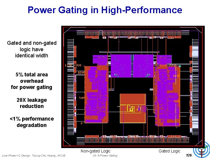
Power Gating in High-Performance Gated and non-gated logic have identical width 5% total area overhead for power gating 20 X leakage reduction <1% performance degradation Non-gated Logic Low-Power IC Design. Tsung-Chu Huang, NCUE Ch. 9 Power-Gating Gated Logic 126 NCUE EDAT

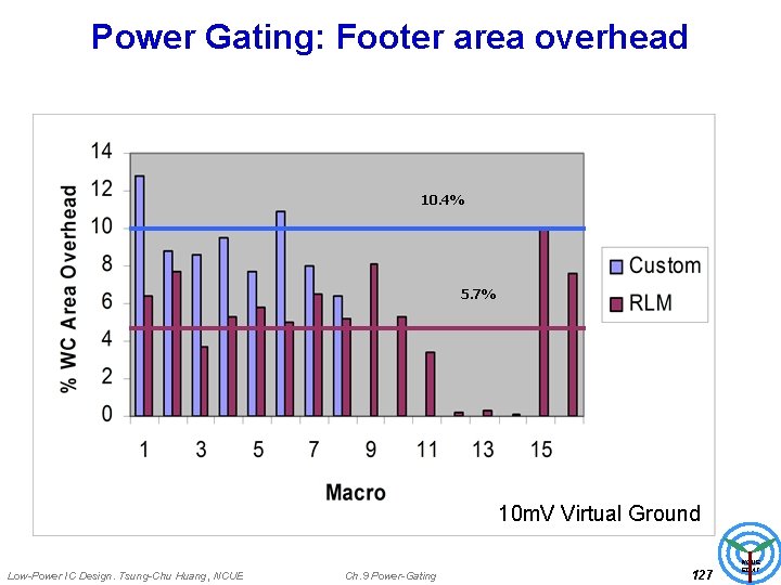
Power Gating: Footer area overhead 10. 4% 5. 7% 10 m. V Virtual Ground Low-Power IC Design. Tsung-Chu Huang, NCUE Ch. 9 Power-Gating 127 NCUE EDAT

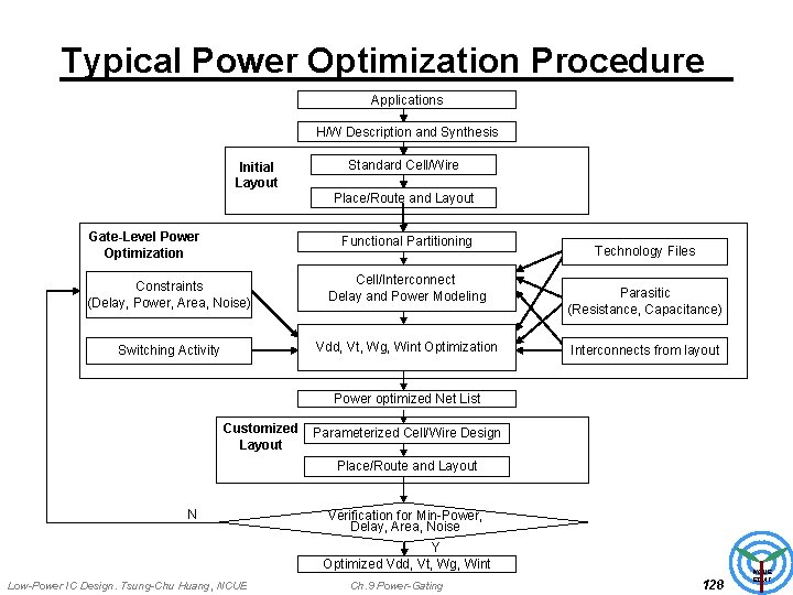
Typical Power Optimization Procedure Applications H/W Description and Synthesis Initial Layout Standard Cell/Wire Place/Route and Layout Gate-Level Power Optimization Functional Partitioning Constraints (Delay, Power, Area, Noise) Cell/Interconnect Delay and Power Modeling Switching Activity Vdd, Vt, Wg, Wint Optimization Technology Files Parasitic (Resistance, Capacitance) Interconnects from layout Power optimized Net List Customized Layout Parameterized Cell/Wire Design Place/Route and Layout N Verification for Min-Power, Delay, Area, Noise Y Optimized Vdd, Vt, Wg, Wint Low-Power IC Design. Tsung-Chu Huang, NCUE Ch. 9 Power-Gating 128 NCUE EDAT