LowPower Design of Digital VLSI Circuits GateLevel Power

![Threshold Voltage Vth = Vt 0 + γ[(Φs+Vsb)½ – Φs½] l Vt 0 is Threshold Voltage Vth = Vt 0 + γ[(Φs+Vsb)½ – Φs½] l Vt 0 is](https://slidetodoc.com/presentation_image_h2/3c3a66f97bd935e89d8b1d698ccfd7e3/image-40.jpg)
- Slides: 59

Low-Power Design of Digital VLSI Circuits Gate-Level Power Optimization Vishwani D. Agrawal James J. Danaher Professor Dept. of Electrical and Computer Engineering Auburn University, Auburn, AL 36849 vagrawal@eng. auburn. edu http: //www. eng. auburn. edu/~vagrawal Copyright Agrawal, 2011 Lectures 11 -14: Gate-level optimization 1

Components of Power l Dynamic l Signal transitions l Logic activity l Glitches l Short-circuit l (often neglected) Static l Leakage Copyright Agrawal, 2011 Lectures 11 -14: Gate-level optimization 2

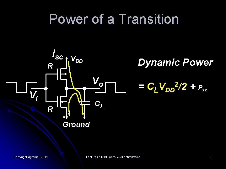
Power of a Transition isc R VDD Dynamic Power Vo Vi = CLVDD 2/2 + Psc CL R Ground Copyright Agrawal, 2011 Lectures 11 -14: Gate-level optimization 3

Dynamic Power Each transition of a gate consumes CV 2/2. l Methods of power saving: l l Minimize load capacitances l Transistor sizing l Library-based gate selection l Reduce transitions l Logic design l Glitch reduction Copyright Agrawal, 2011 Lectures 11 -14: Gate-level optimization 4

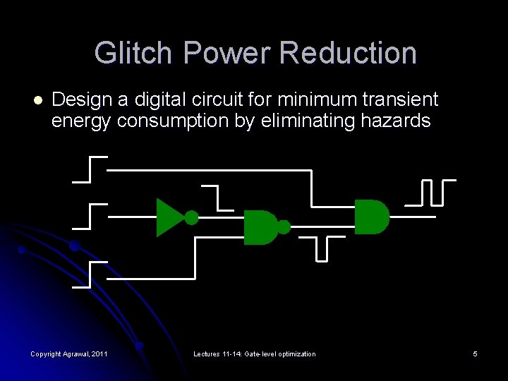
Glitch Power Reduction l Design a digital circuit for minimum transient energy consumption by eliminating hazards Copyright Agrawal, 2011 Lectures 11 -14: Gate-level optimization 5

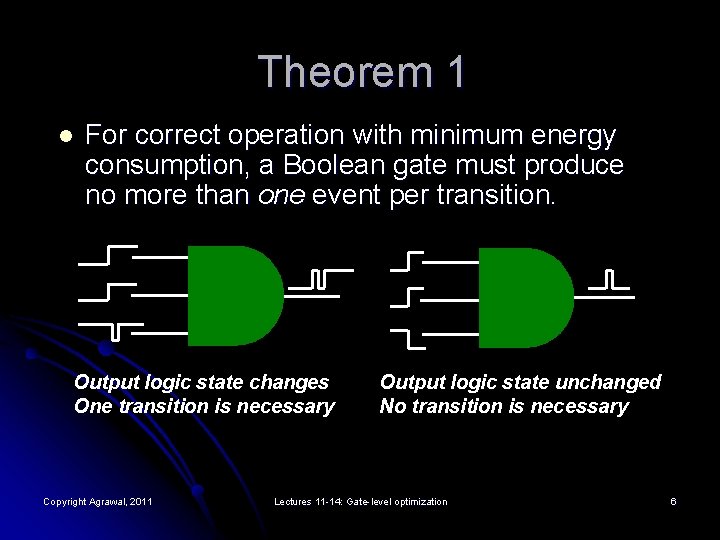
Theorem 1 l For correct operation with minimum energy consumption, a Boolean gate must produce no more than one event per transition. Output logic state changes One transition is necessary Copyright Agrawal, 2011 Output logic state unchanged No transition is necessary Lectures 11 -14: Gate-level optimization 6

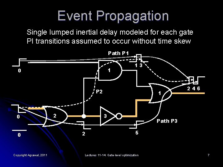
Event Propagation Single lumped inertial delay modeled for each gate PI transitions assumed to occur without time skew Path P 1 1 0 13 P 2 0 0 Copyright Agrawal, 2011 2 1 3 2 246 Path P 3 5 Lectures 11 -14: Gate-level optimization 7

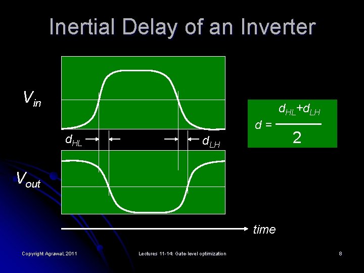
Inertial Delay of an Inverter Vin d. HL+d. LH d. HL d = ──── 2 d. LH Vout time Copyright Agrawal, 2011 Lectures 11 -14: Gate-level optimization 8

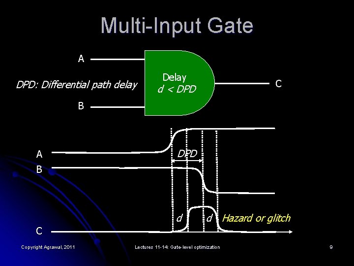
Multi-Input Gate A DPD: Differential path delay Delay C d < DPD B A DPD B d d Hazard or glitch C Copyright Agrawal, 2011 Lectures 11 -14: Gate-level optimization 9

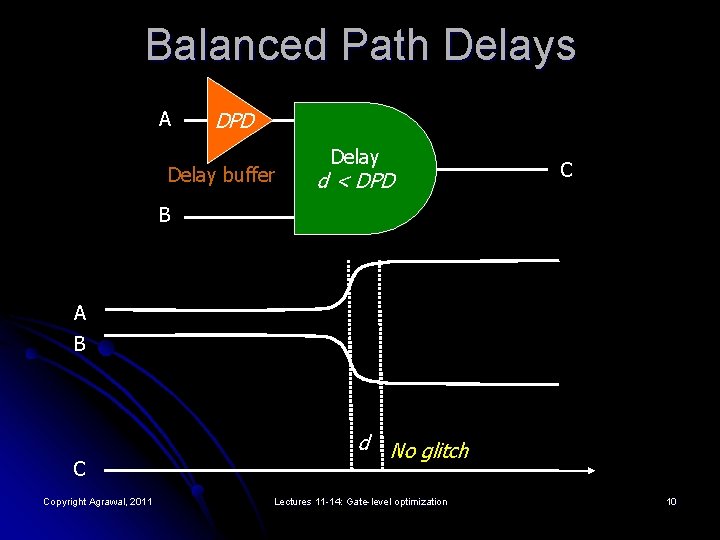
Balanced Path Delays A DPD Delay buffer Delay d < DPD C B A B C Copyright Agrawal, 2011 d No glitch Lectures 11 -14: Gate-level optimization 10

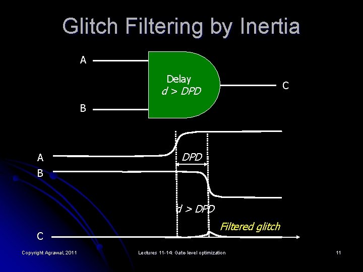
Glitch Filtering by Inertia A Delay d > DPD C B A DPD B d > DPD C Copyright Agrawal, 2011 Filtered glitch Lectures 11 -14: Gate-level optimization 11

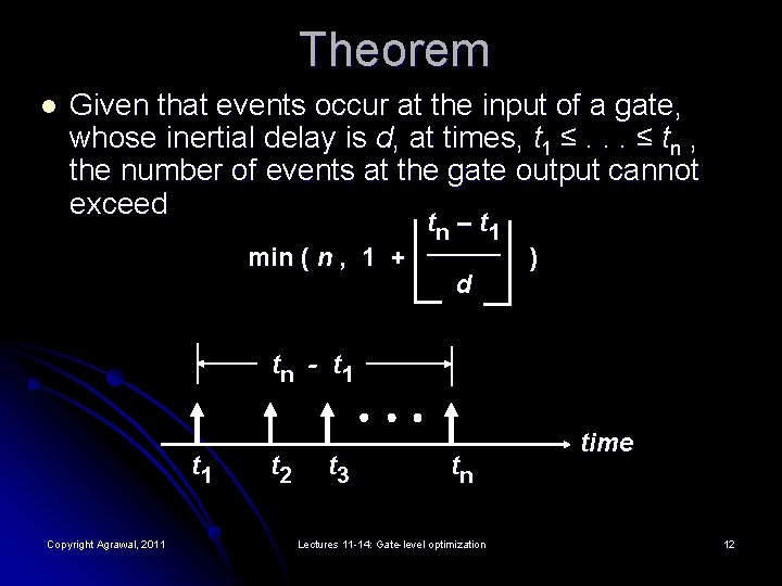
Theorem l Given that events occur at the input of a gate, whose inertial delay is d, at times, t 1 ≤. . . ≤ tn , the number of events at the gate output cannot exceed tn – t 1 min ( n , 1 + ──── d ) tn - t 1 Copyright Agrawal, 2011 t 2 t 3 tn Lectures 11 -14: Gate-level optimization time 12

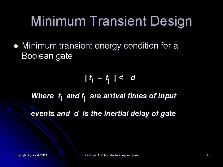
Minimum Transient Design l Minimum transient energy condition for a Boolean gate: | ti – t j | < d Where ti and tj are arrival times of input events and d is the inertial delay of gate Copyright Agrawal, 2011 Lectures 11 -14: Gate-level optimization 13

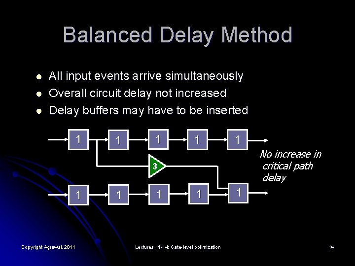
Balanced Delay Method l l l All input events arrive simultaneously Overall circuit delay not increased Delay buffers may have to be inserted 1 1 1 No increase in critical path delay 3 1 Copyright Agrawal, 2011 1 Lectures 11 -14: Gate-level optimization 1 14

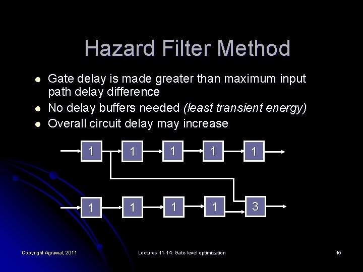
Hazard Filter Method l l l Gate delay is made greater than maximum input path delay difference No delay buffers needed (least transient energy) Overall circuit delay may increase Copyright Agrawal, 2011 1 1 1 1 3 Lectures 11 -14: Gate-level optimization 15

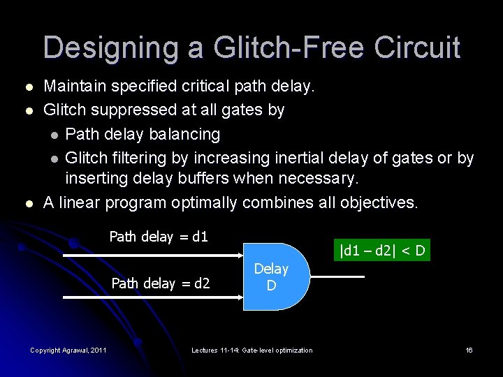
Designing a Glitch-Free Circuit l l l Maintain specified critical path delay. Glitch suppressed at all gates by l Path delay balancing l Glitch filtering by increasing inertial delay of gates or by inserting delay buffers when necessary. A linear program optimally combines all objectives. Path delay = d 1 Path delay = d 2 Copyright Agrawal, 2011 |d 1 – d 2| < D Delay D Lectures 11 -14: Gate-level optimization 16

Problem Complexity l Number of paths in a circuit can be exponential in circuit size. l Considering all paths through enumeration is infeasible for large circuits. l Example: c 880 has 6. 96 M path constraints. Copyright Agrawal, 2011 Lectures 11 -14: Gate-level optimization 17

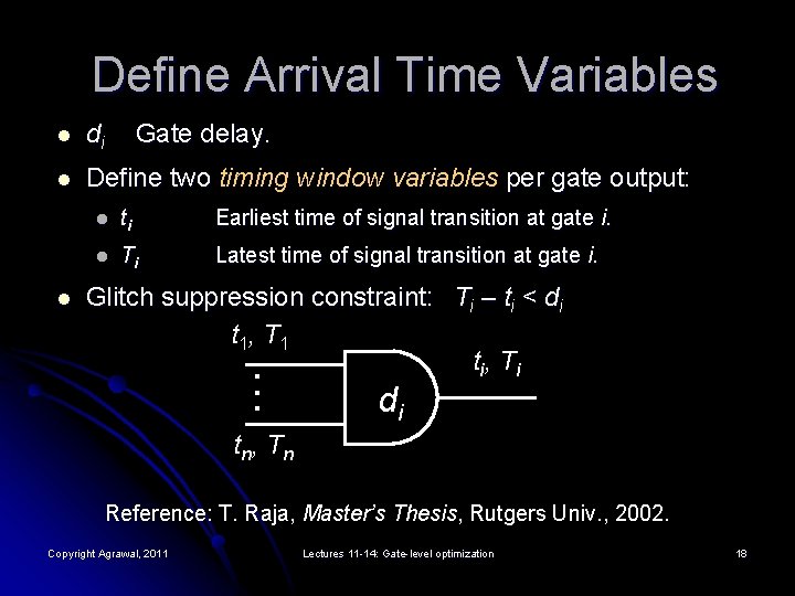
Define Arrival Time Variables l di l Define two timing window variables per gate output: l Gate delay. l ti Earliest time of signal transition at gate i. l Ti Latest time of signal transition at gate i. Glitch suppression constraint: Ti – ti < di t 1, T 1 t i, T i. . . di t n, T n Reference: T. Raja, Master’s Thesis, Rutgers Univ. , 2002. Copyright Agrawal, 2011 Lectures 11 -14: Gate-level optimization 18

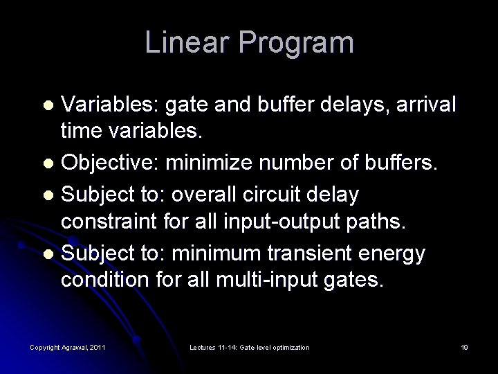
Linear Program Variables: gate and buffer delays, arrival time variables. l Objective: minimize number of buffers. l Subject to: overall circuit delay constraint for all input-output paths. l Subject to: minimum transient energy condition for all multi-input gates. l Copyright Agrawal, 2011 Lectures 11 -14: Gate-level optimization 19

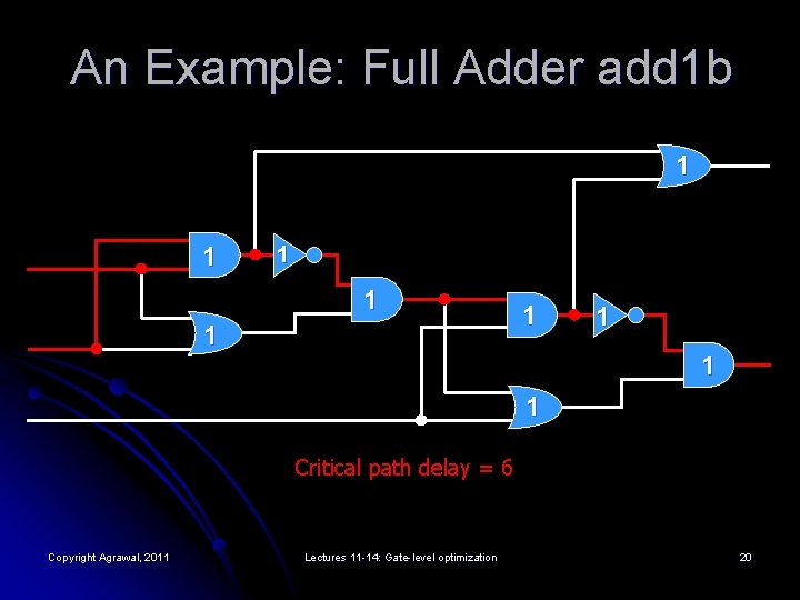
An Example: Full Adder add 1 b 1 1 1 1 1 Critical path delay = 6 Copyright Agrawal, 2011 Lectures 11 -14: Gate-level optimization 20

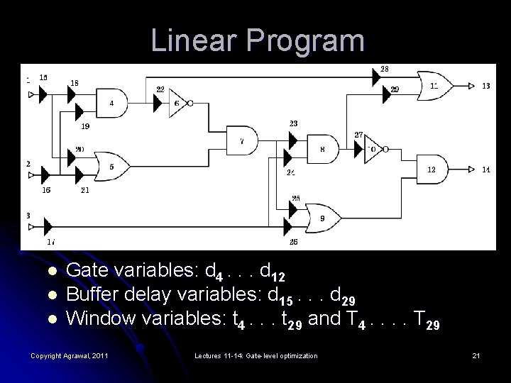
Linear Program l l l Gate variables: d 4. . . d 12 Buffer delay variables: d 15. . . d 29 Window variables: t 4. . . t 29 and T 4. . T 29 Copyright Agrawal, 2011 Lectures 11 -14: Gate-level optimization 21

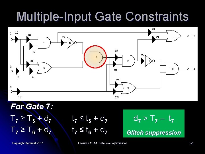
Multiple-Input Gate Constraints For Gate 7: T 7 ≥ T 5 + d 7 T 7 ≥ T 6 + d 7 Copyright Agrawal, 2011 t 7 ≤ t 5 + d 7 t 7 ≤ t 6 + d 7 > T 7 – t 7 Glitch suppression Lectures 11 -14: Gate-level optimization 22

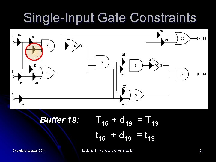
Single-Input Gate Constraints Buffer 19: T 16 + d 19 = T 19 t 16 + d 19 = t 19 Copyright Agrawal, 2011 Lectures 11 -14: Gate-level optimization 23

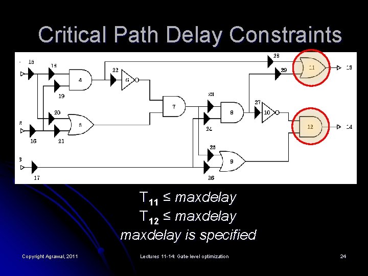
Critical Path Delay Constraints T 11 ≤ maxdelay T 12 ≤ maxdelay is specified Copyright Agrawal, 2011 Lectures 11 -14: Gate-level optimization 24

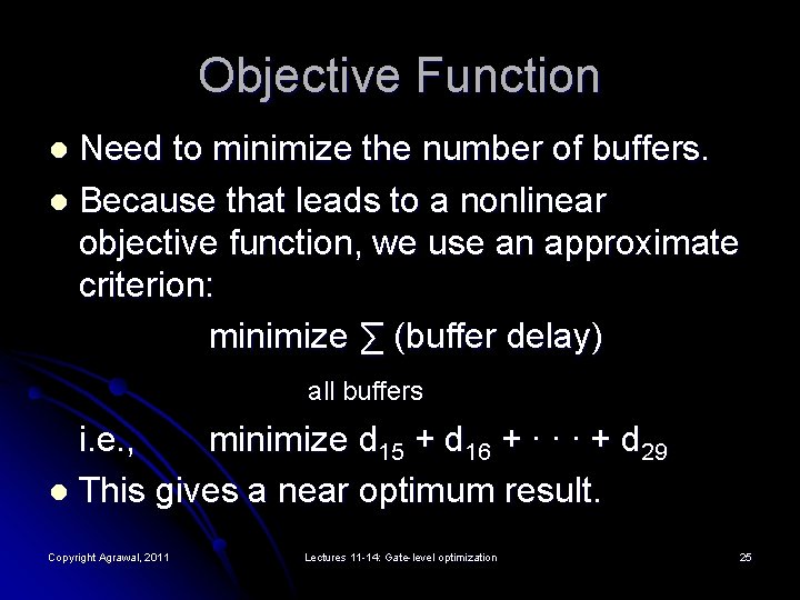
Objective Function Need to minimize the number of buffers. l Because that leads to a nonlinear objective function, we use an approximate criterion: minimize ∑ (buffer delay) l all buffers i. e. , minimize d 15 + d 16 + ∙ ∙ ∙ + d 29 l This gives a near optimum result. Copyright Agrawal, 2011 Lectures 11 -14: Gate-level optimization 25

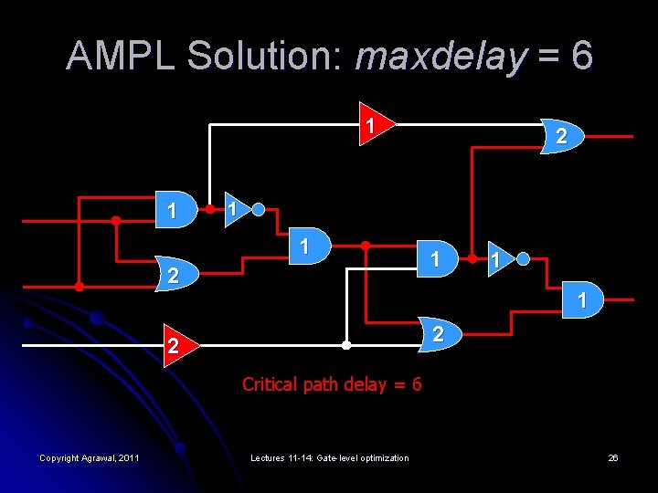
AMPL Solution: maxdelay = 6 1 1 2 1 1 1 2 2 Critical path delay = 6 Copyright Agrawal, 2011 Lectures 11 -14: Gate-level optimization 26

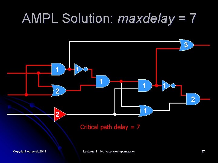
AMPL Solution: maxdelay = 7 3 1 1 1 2 1 2 Critical path delay = 7 Copyright Agrawal, 2011 Lectures 11 -14: Gate-level optimization 27

AMPL Solution: maxdelay ≥ 11 5 1 1 1 2 3 1 3 4 Critical path delay = 11 Copyright Agrawal, 2011 Lectures 11 -14: Gate-level optimization 28

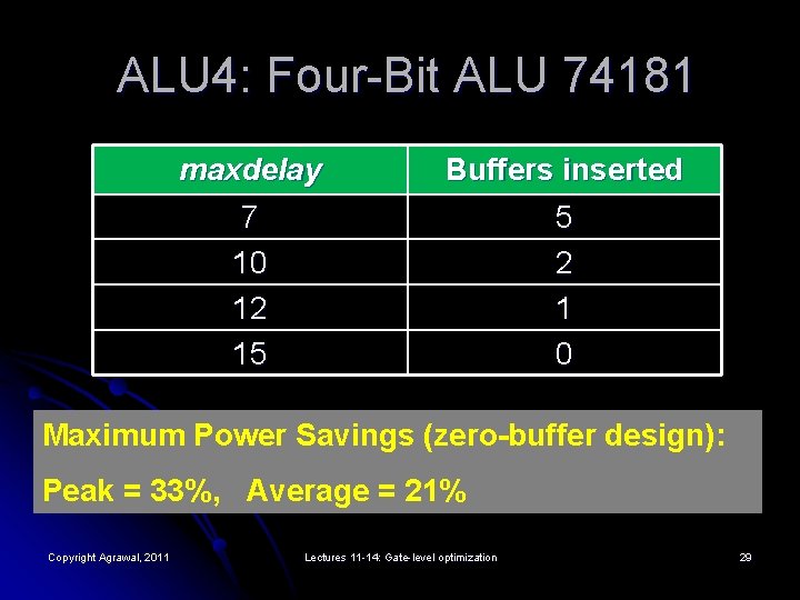
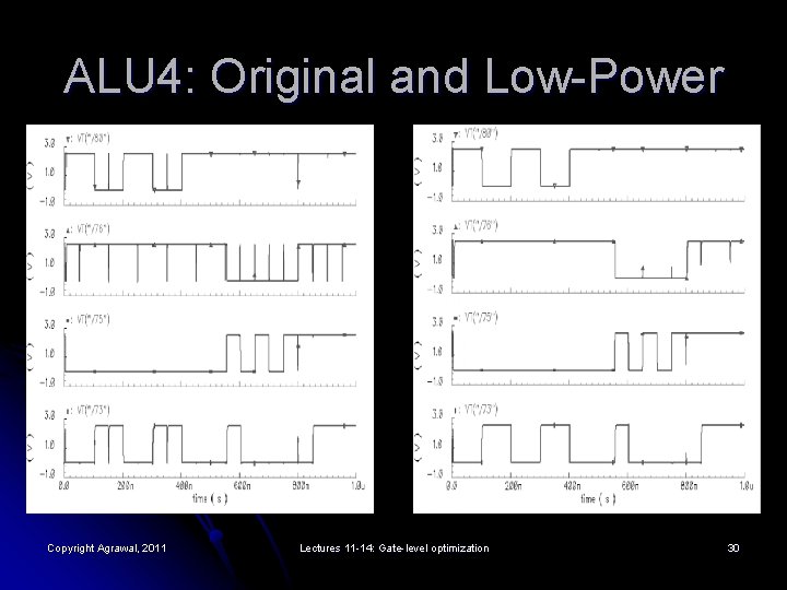
ALU 4: Four-Bit ALU 74181 maxdelay Buffers inserted 7 10 12 15 5 2 1 0 Maximum Power Savings (zero-buffer design): Peak = 33%, Average = 21% Copyright Agrawal, 2011 Lectures 11 -14: Gate-level optimization 29

ALU 4: Original and Low-Power Copyright Agrawal, 2011 Lectures 11 -14: Gate-level optimization 30

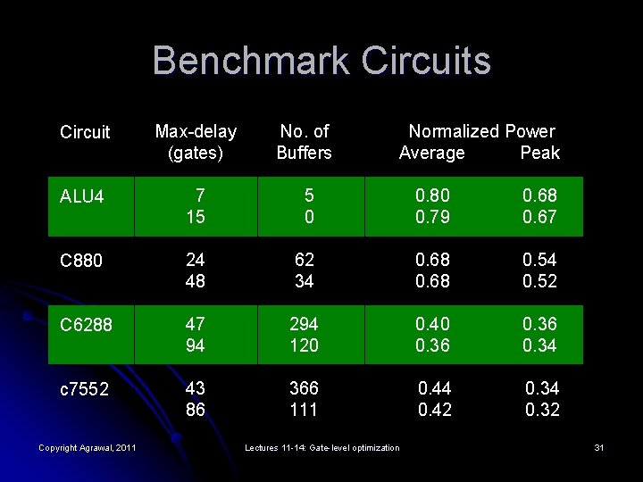
Benchmark Circuits Normalized Power Average Peak Circuit Max-delay (gates) No. of Buffers ALU 4 7 15 5 0 0. 80 0. 79 0. 68 0. 67 C 880 24 48 62 34 0. 68 0. 54 0. 52 C 6288 47 94 294 120 0. 40 0. 36 0. 34 c 7552 43 86 366 111 0. 44 0. 42 0. 34 0. 32 Copyright Agrawal, 2011 Lectures 11 -14: Gate-level optimization 31

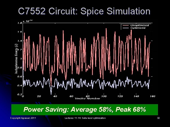
C 7552 Circuit: Spice Simulation Power Saving: Average 58%, Peak 68% Copyright Agrawal, 2011 Lectures 11 -14: Gate-level optimization 32

References l l l l R. Fourer, D. M. Gay and B. W. Kernighan, AMPL: A Modeling Language for Mathematical Programming, South San Francisco: The Scientific Press, 1993. M. Berkelaar and E. Jacobs, “Using Gate Sizing to Reduce Glitch Power, ” Proc. Pro. RISC Workshop, Mierlo, The Netherlands, Nov. 1996, pp. 183 -188. V. D. Agrawal, “Low Power Design by Hazard Filtering, ” Proc. 10 th Int’l Conf. VLSI Design, Jan. 1997, pp. 193 -197. V. D. Agrawal, M. L. Bushnell, G. Parthasarathy and R. Ramadoss, “Digital Circuit Design for Minimum Transient Energy and Linear Programming Method, ” Proc. 12 th Int’l Conf. VLSI Design, Jan. 1999, pp. 434 -439. T. Raja, V. D. Agrawal and M. L. Bushnell, “Minimum Dynamic Power CMOS Circuit Design by a Reduced Constraint Set Linear Program, ” Proc. 16 th Int’l Conf. VLSI Design, Jan. 2003, pp. 527 -532. T. Raja, V. D. Agrawal, and M. L. Bushnell, “Transistor sizing of logicgates to maximize input delay variability, ” J. Low Power Electron. , vol. 2, no. 1, pp. 121– 128, Apr. 2006. T. Raja, V. D. Agrawal, and M. L. Bushnell, “Variable Input Delay CMOS Logic for Low Power Design, ” IEEE Trans. VLSI Design, vol. 17, mo. 10, pp. 15341545. October 2009. Copyright Agrawal, 2011 Lectures 11 -14: Gate-level optimization 33

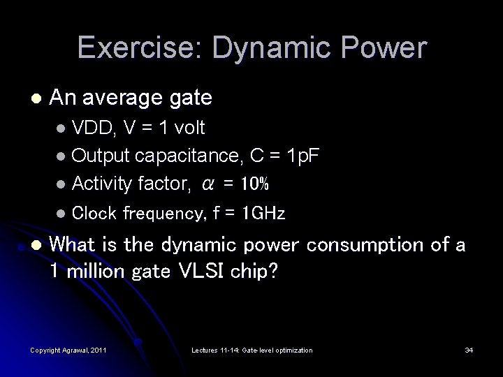
Exercise: Dynamic Power l An average gate l VDD, V = 1 volt l Output capacitance, C = 1 p. F l Activity factor, α = 10% l Clock frequency, f = 1 GHz l What is the dynamic power consumption of a 1 million gate VLSI chip? Copyright Agrawal, 2011 Lectures 11 -14: Gate-level optimization 34

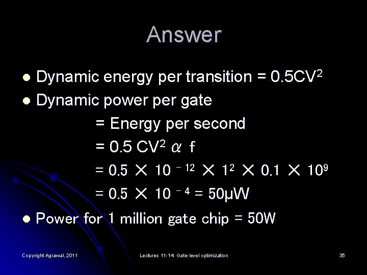
Answer Dynamic energy per transition = 0. 5 CV 2 l Dynamic power per gate = Energy per second = 0. 5 CV 2 α f = 0. 5 ✕ 10 – 12 ✕ 0. 1 ✕ 109 = 0. 5 ✕ 10 – 4 = 50μW l Power for 1 million gate chip = 50 W l Copyright Agrawal, 2011 Lectures 11 -14: Gate-level optimization 35

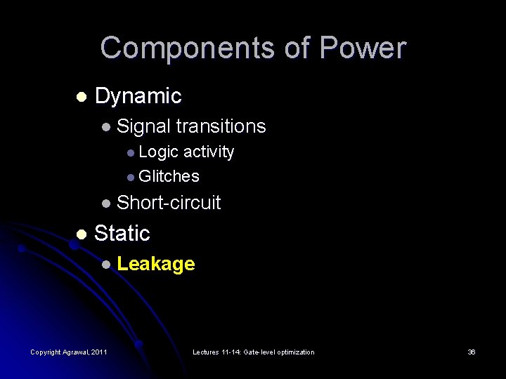
Components of Power l Dynamic l Signal transitions l Logic activity l Glitches l Short-circuit l Static l Copyright Agrawal, 2011 Leakage Lectures 11 -14: Gate-level optimization 36

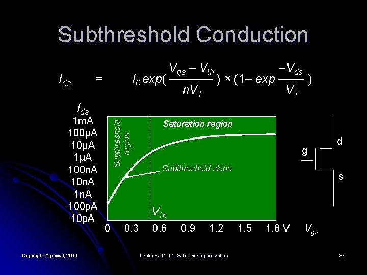
Subthreshold Conduction Ids Vgs – Vth –Vds I 0 exp( ───── ) × (1– exp ─── ) n. VT VT = 1 m. A 100μA 1μA 100 n. A 1 n. A 100 p. A 10 p. A Copyright Agrawal, 2011 Subthreshold region Ids Saturation region g Subthreshold slope d s Vth 0 0. 3 0. 6 0. 9 1. 2 Lectures 11 -14: Gate-level optimization 1. 5 1. 8 V Vgs 37

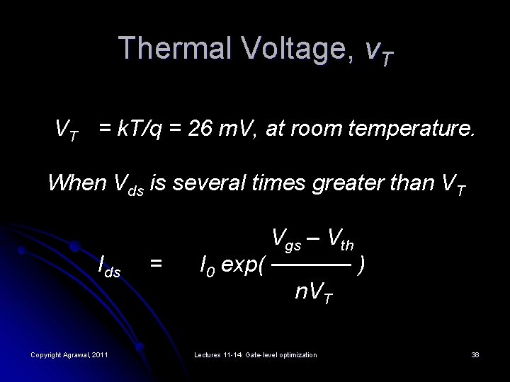
Thermal Voltage, v. T VT = k. T/q = 26 m. V, at room temperature. When Vds is several times greater than VT Ids Copyright Agrawal, 2011 = Vgs – Vth I 0 exp( ───── ) n. VT Lectures 11 -14: Gate-level optimization 38

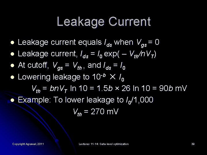
Leakage Current l l l Leakage current equals Ids when Vgs = 0 Leakage current, Ids = I 0 exp( – Vth/n. VT) At cutoff, Vgs = Vth , and Ids = I 0 Lowering leakage to 10 -b ✕ I 0 Vth = bn. VT ln 10 = 1. 5 b × 26 ln 10 = 90 b m. V Example: To lower leakage to I 0/1, 000 Vth = 270 m. V Copyright Agrawal, 2011 Lectures 11 -14: Gate-level optimization 39
![Threshold Voltage Vth Vt 0 γΦsVsb½ Φs½ l Vt 0 is Threshold Voltage Vth = Vt 0 + γ[(Φs+Vsb)½ – Φs½] l Vt 0 is](https://slidetodoc.com/presentation_image_h2/3c3a66f97bd935e89d8b1d698ccfd7e3/image-40.jpg)
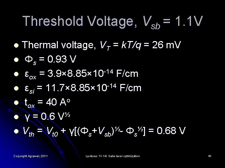
Threshold Voltage Vth = Vt 0 + γ[(Φs+Vsb)½ – Φs½] l Vt 0 is threshold voltage when source is at body potential (0. 4 V for 180 nm process) ( l Φs = 2 VT ln(NA /ni ) is surface potential l γ = (2 qεsi NA)½tox /εox is body effect coefficient (0. 4 to 1. 0) l NA is doping level = 8× 1017 cm– 3 l ni = 1. 45× 1010 cm– 3 l Copyright Agrawal, 2011 Lectures 11 -14: Gate-level optimization 40

Threshold Voltage, Vsb = 1. 1 V Thermal voltage, VT = k. T/q = 26 m. V l Φs = 0. 93 V l εox = 3. 9× 8. 85× 10 -14 F/cm l εsi = 11. 7× 8. 85× 10 -14 F/cm l tox = 40 Ao l γ = 0. 6 V½ l Vth = Vt 0 + γ[(Φs+Vsb)½- Φs½] = 0. 68 V l Copyright Agrawal, 2011 Lectures 11 -14: Gate-level optimization 41

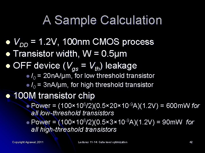
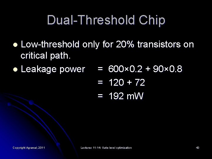
A Sample Calculation VDD = 1. 2 V, 100 nm CMOS process l Transistor width, W = 0. 5μm l OFF device (Vgs = Vth) leakage l l I 0 = 20 n. A/μm, for low threshold transistor l I 0 = 3 n. A/μm, for high threshold transistor l 100 M transistor chip l Power = (100× 106/2)(0. 5× 20× 10 -9 A)(1. 2 V) = 600 m. W for all low-threshold transistors l Power = (100× 106/2)(0. 5× 3× 10 -9 A)(1. 2 V) = 90 m. W for all high-threshold transistors Copyright Agrawal, 2011 Lectures 11 -14: Gate-level optimization 42

Dual-Threshold Chip Low-threshold only for 20% transistors on critical path. l Leakage power = 600× 0. 2 + 90× 0. 8 = 120 + 72 = 192 m. W l Copyright Agrawal, 2011 Lectures 11 -14: Gate-level optimization 43

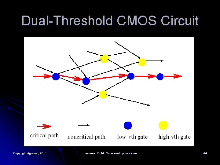
Dual-Threshold CMOS Circuit Copyright Agrawal, 2011 Lectures 11 -14: Gate-level optimization 44

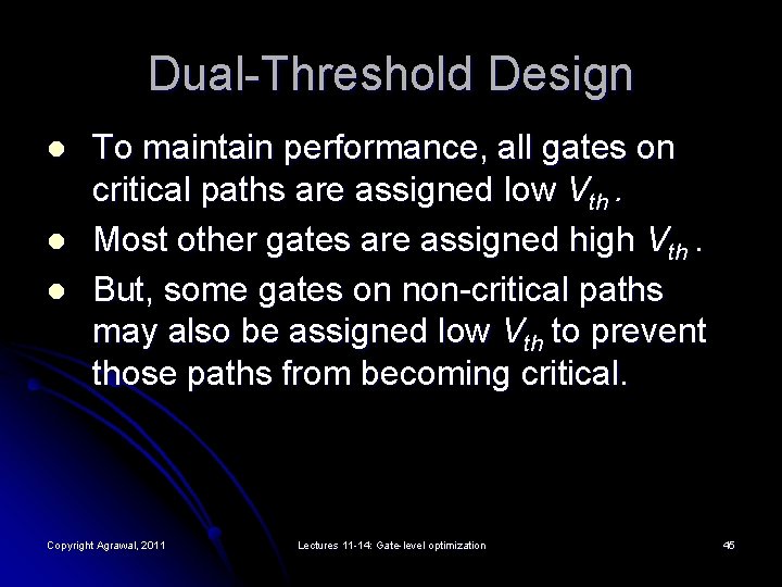
Dual-Threshold Design l l l To maintain performance, all gates on critical paths are assigned low Vth. Most other gates are assigned high Vth. But, some gates on non-critical paths may also be assigned low Vth to prevent those paths from becoming critical. Copyright Agrawal, 2011 Lectures 11 -14: Gate-level optimization 45

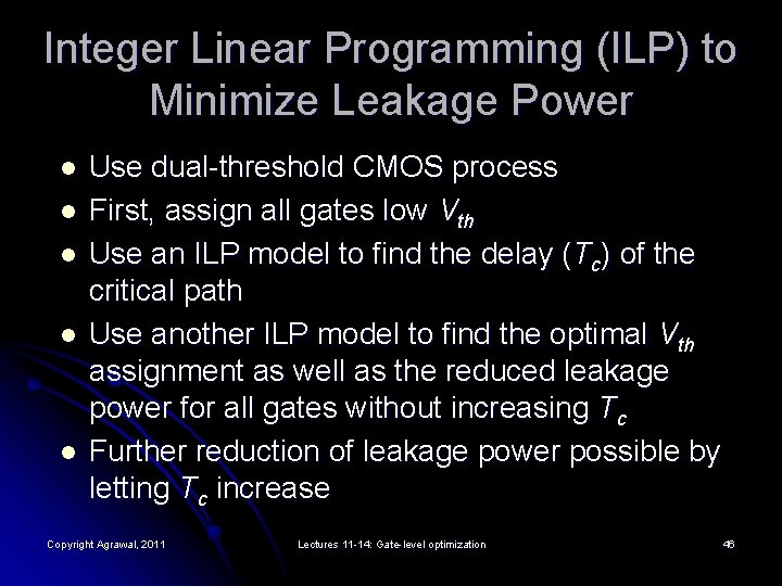
Integer Linear Programming (ILP) to Minimize Leakage Power l l l Use dual-threshold CMOS process First, assign all gates low Vth Use an ILP model to find the delay (Tc) of the critical path Use another ILP model to find the optimal Vth assignment as well as the reduced leakage power for all gates without increasing Tc Further reduction of leakage power possible by letting Tc increase Copyright Agrawal, 2011 Lectures 11 -14: Gate-level optimization 46

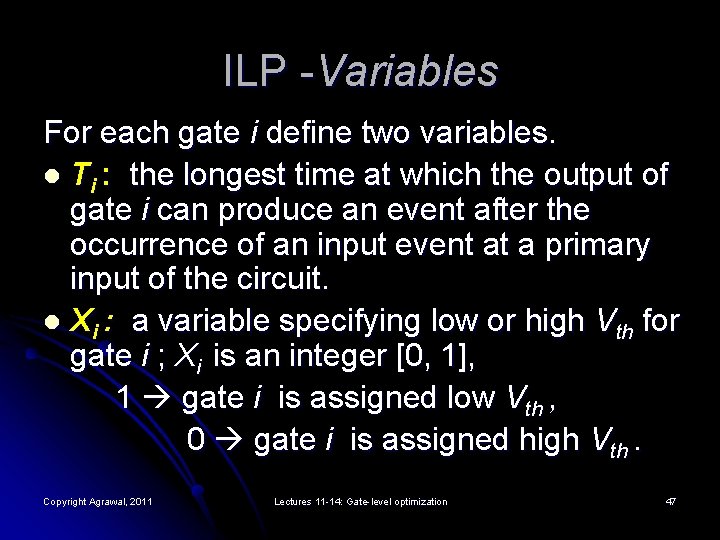
ILP -Variables For each gate i define two variables. l Ti : the longest time at which the output of gate i can produce an event after the occurrence of an input event at a primary input of the circuit. l Xi : a variable specifying low or high Vth for gate i ; Xi is an integer [0, 1], 1 gate i is assigned low Vth , 0 gate i is assigned high Vth. Copyright Agrawal, 2011 Lectures 11 -14: Gate-level optimization 47

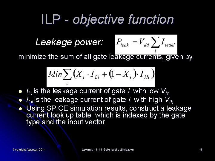
ILP - objective function Leakage power: minimize the sum of all gate leakage currents, given by l l l ILi is the leakage current of gate i with low Vth IHi is the leakage current of gate i with high Vth Using SPICE simulation results, construct a leakage current look up table, which is indexed by the gate type and the input vector. Copyright Agrawal, 2011 Lectures 11 -14: Gate-level optimization 48

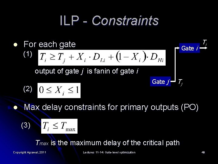
ILP - Constraints l For each gate Gate i (1) Ti output of gate j is fanin of gate i Gate j (2) l Tj Max delay constraints for primary outputs (PO) (3) Tmax is the maximum delay of the critical path Copyright Agrawal, 2011 Lectures 11 -14: Gate-level optimization 49

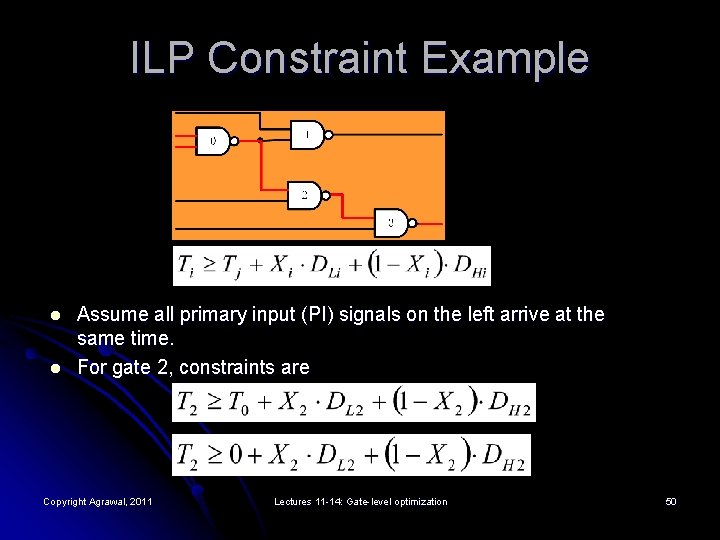
ILP Constraint Example l l Assume all primary input (PI) signals on the left arrive at the same time. For gate 2, constraints are Copyright Agrawal, 2011 Lectures 11 -14: Gate-level optimization 50

ILP – Constraints (cont. ) DHi is the delay of gate i with high Vth l DLi is the delay of gate i with low Vth l A second look-up table is constructed and specifies the delay for given gate types and fanout numbers. l Copyright Agrawal, 2011 Lectures 11 -14: Gate-level optimization 51

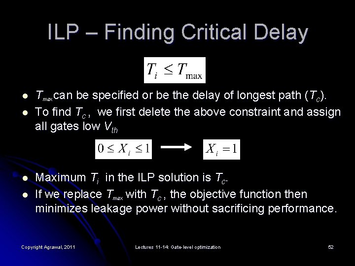
ILP – Finding Critical Delay l l Tmax can be specified or be the delay of longest path (Tc). To find Tc , we first delete the above constraint and assign all gates low Vth Maximum Ti in the ILP solution is Tc. If we replace Tmax with Tc , the objective function then minimizes leakage power without sacrificing performance. Copyright Agrawal, 2011 Lectures 11 -14: Gate-level optimization 52

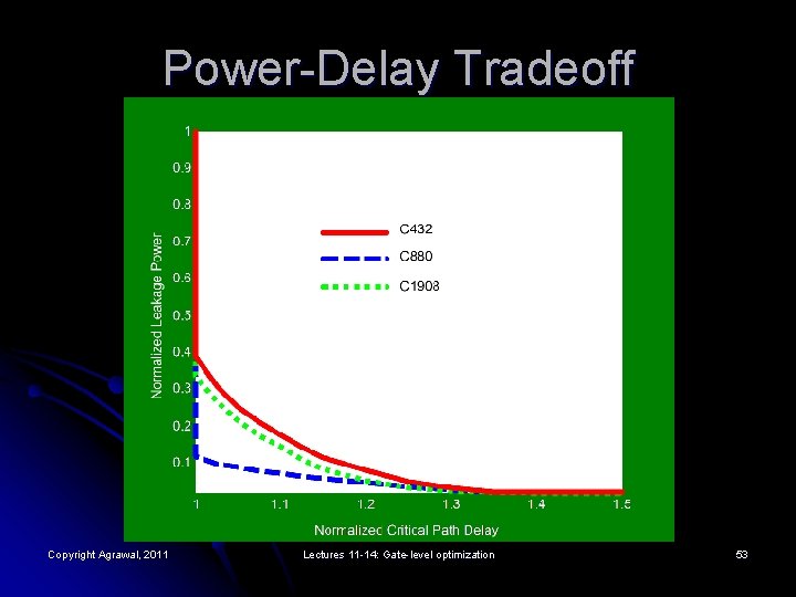
Power-Delay Tradeoff Copyright Agrawal, 2011 Lectures 11 -14: Gate-level optimization 53

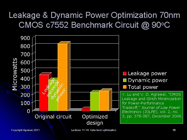
Power-Delay Tradeoff l l If we gradually increase Tmax from Tc , leakage power is further reduced, because more gates can be assigned high Vth. But, the reduction trends to become slower. When Tmax = (130%) Tc , the reduction about levels off because almost all gates are assigned high Vth. Maximum leakage reduction can be 98%. Copyright Agrawal, 2011 Lectures 11 -14: Gate-level optimization 54

Le ex ak dy cee age po nam ds w er ic Leakage & Dynamic Power Optimization 70 nm CMOS c 7552 Benchmark Circuit @ 90 o. C Copyright Agrawal, 2011 Y. Lu and V. D. Agrawal, “CMOS Leakage and Glitch Minimization for Power-Performance Tradeoff, ” Journal of Low Power Electronics (JOLPE), vol. 2, no. 3, pp. 378 -387, December 2006. Lectures 11 -14: Gate-level optimization 55

Summary l l l Leakage power is a significant fraction of the total power in nanometer CMOS devices. Leakage power increases with temperature; can be as much as dynamic power. Dual threshold design can reduce leakage. l l Reference: Y. Lu and V. D. Agrawal, “CMOS Leakage and Glitch Minimization for Power-Performance Tradeoff, ” J. Low Power Electronics, Vol. 2, No. 3, pp. 378 -387, December 2006. Access other paper at http: //www. eng. auburn. edu/~vagrawal/TALKS/talks. html Copyright Agrawal, 2011 Lectures 11 -14: Gate-level optimization 56

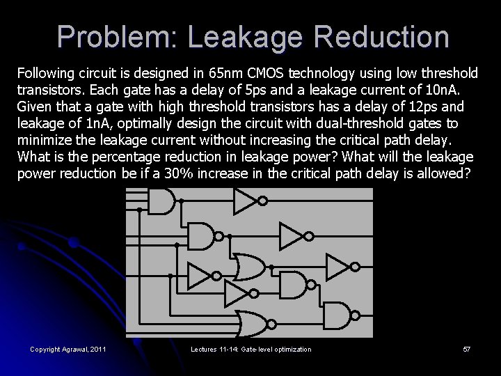
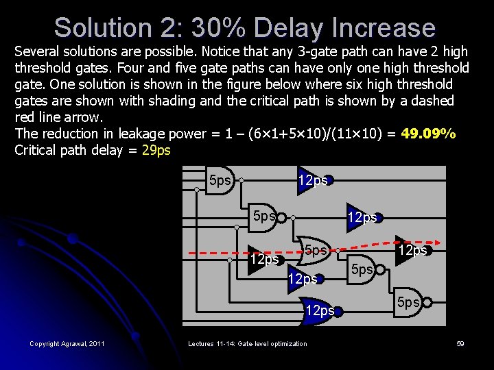
Problem: Leakage Reduction Following circuit is designed in 65 nm CMOS technology using low threshold transistors. Each gate has a delay of 5 ps and a leakage current of 10 n. A. Given that a gate with high threshold transistors has a delay of 12 ps and leakage of 1 n. A, optimally design the circuit with dual-threshold gates to minimize the leakage current without increasing the critical path delay. What is the percentage reduction in leakage power? What will the leakage power reduction be if a 30% increase in the critical path delay is allowed? Copyright Agrawal, 2011 Lectures 11 -14: Gate-level optimization 57

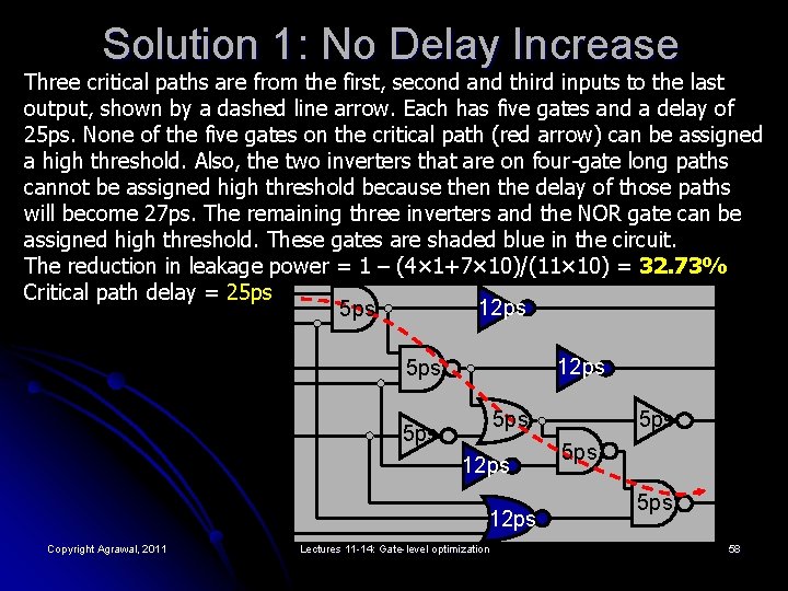
Solution 1: No Delay Increase Three critical paths are from the first, second and third inputs to the last output, shown by a dashed line arrow. Each has five gates and a delay of 25 ps. None of the five gates on the critical path (red arrow) can be assigned a high threshold. Also, the two inverters that are on four-gate long paths cannot be assigned high threshold because then the delay of those paths will become 27 ps. The remaining three inverters and the NOR gate can be assigned high threshold. These gates are shaded blue in the circuit. The reduction in leakage power = 1 – (4× 1+7× 10)/(11× 10) = 32. 73% Critical path delay = 25 ps 12 ps 5 ps 5 ps 12 ps Copyright Agrawal, 2011 Lectures 11 -14: Gate-level optimization 5 ps 5 ps 58

Solution 2: 30% Delay Increase Several solutions are possible. Notice that any 3 -gate path can have 2 high threshold gates. Four and five gate paths can have only one high threshold gate. One solution is shown in the figure below where six high threshold gates are shown with shading and the critical path is shown by a dashed red line arrow. The reduction in leakage power = 1 – (6× 1+5× 10)/(11× 10) = 49. 09% Critical path delay = 29 ps 5 ps 12 ps 5 ps 12 ps Copyright Agrawal, 2011 Lectures 11 -14: Gate-level optimization 12 ps 5 ps 59