LowPower Circuits for a 2 5 V 10

- Slides: 8

Low-Power Circuits for a 2. 5 -V, 10. 7 to-86 -Gb/s Serial Transmitter in 130 nm Si. Ge Bi. CMOS Tod Dickson University of Toronto June 9, 2005

Motivation Ever-growing bandwidth demands results in higher data rate broadband transceivers Next generation wireline applications will exceed 80 -Gb/s. To date, serial transmitters at this data rate have not been demonstrated. High power consumption even an 40 -Gb/s makes high levels of integration difficult. Reducing power consumption without sacrificing speed is a key challenge. T. Dickson University of Toronto June 24, 2005

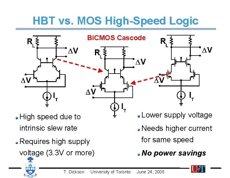
HBT vs. MOS High-Speed Logic Bi. CMOS Cascode Lower supply voltage High speed due to intrinsic slew rate Requires high supply voltage (3. 3 V or more) T. Dickson University of Toronto Needs higher current for same speed No power savings June 24, 2005

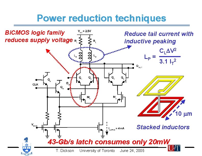
Power reduction techniques Bi. CMOS logic family reduces supply voltage Reduce tail current with inductive peaking LP = CLDV 2 3. 1 IT 2 10 mm Stacked inductors 43 -Gb/s latch consumes only 20 m. W T. Dickson University of Toronto June 24, 2005

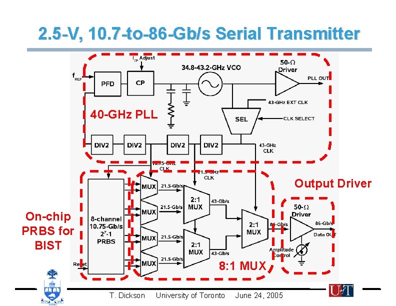
2. 5 -V, 10. 7 -to-86 -Gb/s Serial Transmitter 40 -GHz PLL Output Driver On-chip PRBS for BIST 8: 1 MUX T. Dickson University of Toronto June 24, 2005

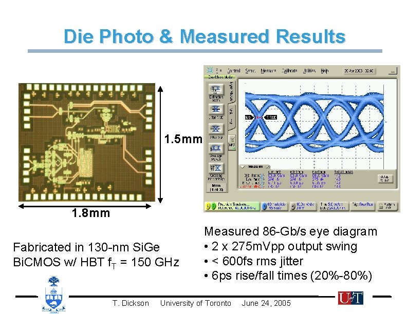
Die Photo & Measured Results 1. 5 mm 1. 8 mm Fabricated in 130 -nm Si. Ge Bi. CMOS w/ HBT f. T = 150 GHz T. Dickson Measured 86 -Gb/s eye diagram • 2 x 275 m. Vpp output swing • < 600 fs rms jitter • 6 ps rise/fall times (20%-80%) University of Toronto June 24, 2005

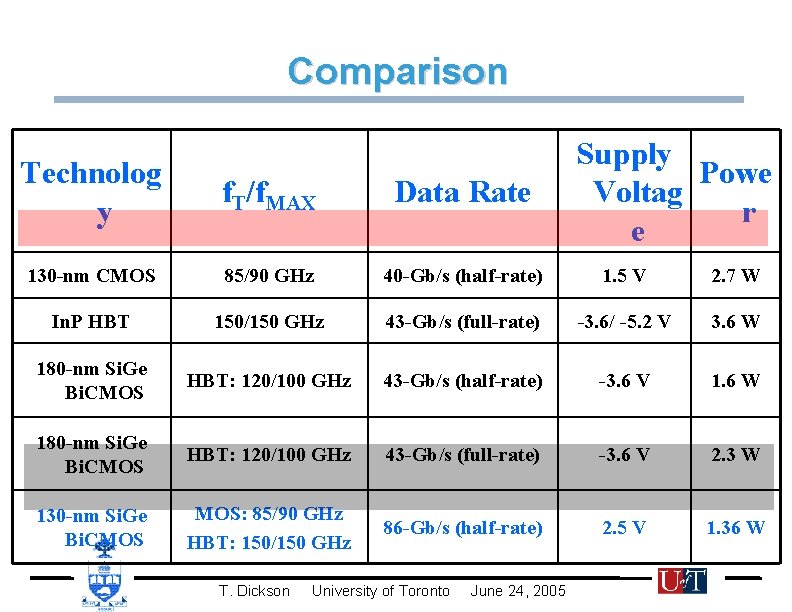
Comparison Supply Powe Voltag r e Technolog y f. T/f. MAX Data Rate 130 -nm CMOS 85/90 GHz 40 -Gb/s (half-rate) 1. 5 V 2. 7 W In. P HBT 150/150 GHz 43 -Gb/s (full-rate) -3. 6/ -5. 2 V 3. 6 W 180 -nm Si. Ge Bi. CMOS HBT: 120/100 GHz 43 -Gb/s (half-rate) -3. 6 V 1. 6 W 180 -nm Si. Ge Bi. CMOS HBT: 120/100 GHz 43 -Gb/s (full-rate) -3. 6 V 2. 3 W 130 -nm Si. Ge Bi. CMOS MOS: 85/90 GHz HBT: 150/150 GHz 86 -Gb/s (half-rate) 2. 5 V 1. 36 W T. Dickson University of Toronto June 24, 2005

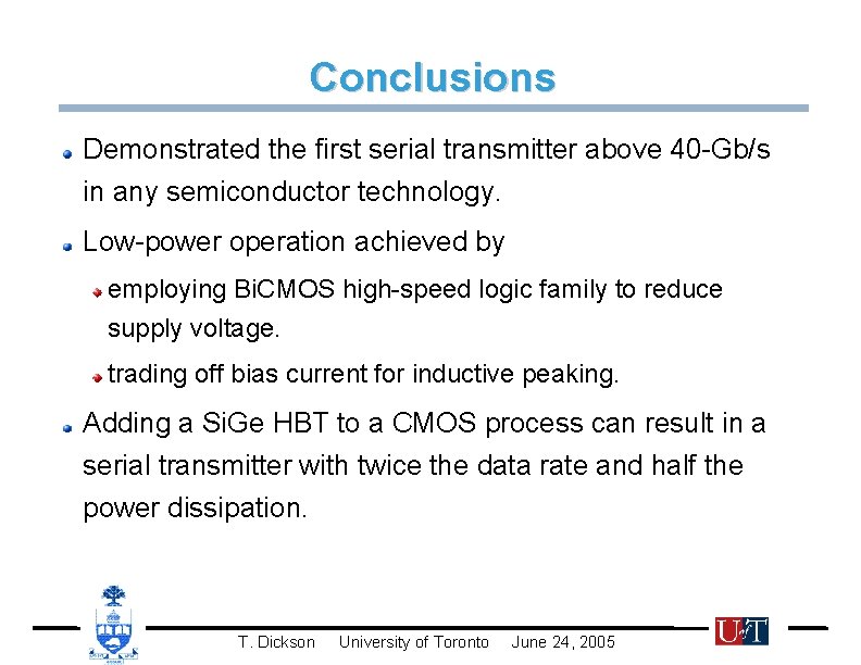
Conclusions Demonstrated the first serial transmitter above 40 -Gb/s in any semiconductor technology. Low-power operation achieved by employing Bi. CMOS high-speed logic family to reduce supply voltage. trading off bias current for inductive peaking. Adding a Si. Ge HBT to a CMOS process can result in a serial transmitter with twice the data rate and half the power dissipation. T. Dickson University of Toronto June 24, 2005