
Lowk Dielectrics Materials and Process Technology Rebeca C
Low-k Dielectrics: Materials and Process Technology Rebeca C. Diaz EE 518, Penn State Instructor: Dr. J. Ruzyllo April 13, 2006
Outline l Motivation for low-k dielectrics l Required properties of low-k dielectrics l Proposed materials l Most promising materials l CVD vs. Spin-on techniques l Conclusion

Why Low-k Dielectrics? l Reduce RC constant without reducing size l R metal interconnect minimized with Cu l C dielectric need low-k

Why Low-k Dielectrics? 2
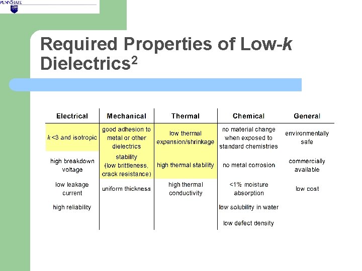
Required Properties of Low-k Dielectrics 2
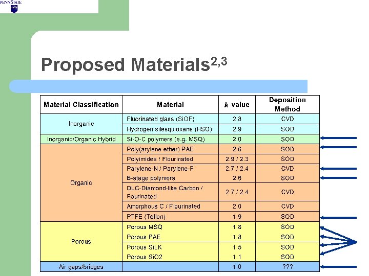
Proposed Materials 2, 3
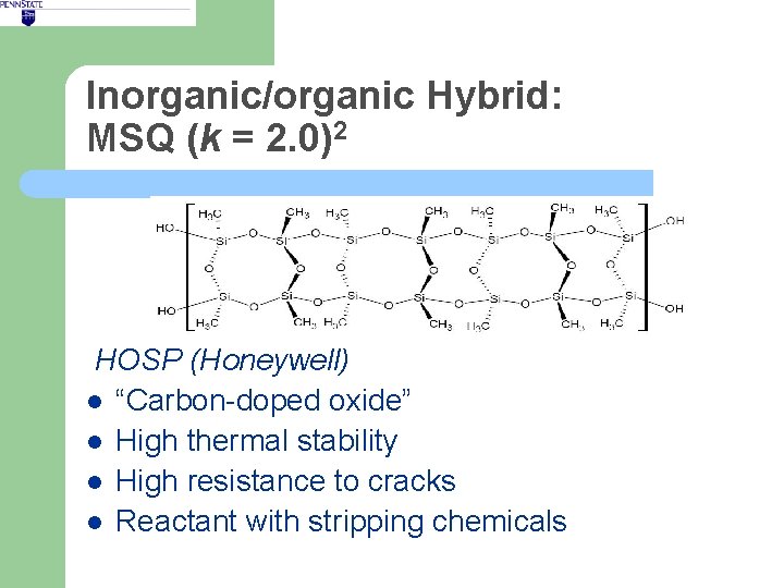
Inorganic/organic Hybrid: MSQ (k = 2. 0)2 HOSP (Honeywell) l “Carbon-doped oxide” l High thermal stability l High resistance to cracks l Reactant with stripping chemicals
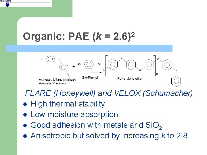
Organic: PAE (k = 2. 6)2 FLARE (Honeywell) and VELOX (Schumacher) l High thermal stability l Low moisture absorption l Good adhesion with metals and Si. O 2 l Anisotropic but solved by increasing k to 2. 8
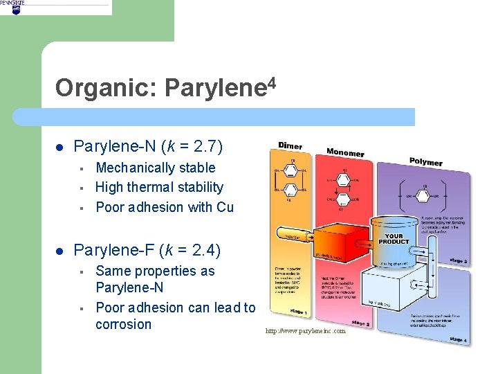
Organic: Parylene 4 l Parylene-N (k = 2. 7) § § § l Mechanically stable High thermal stability Poor adhesion with Cu Parylene-F (k = 2. 4) § § Same properties as Parylene-N Poor adhesion can lead to corrosion http: //www. paryleneinc. com
Organic: B-staged polymers (k = 2. 6)2 CYCLOTENE (Dow Chemical) l l l Fluorine based Good temperature stability Low metal adhesion Moisture absorption Currently used in Ga. As interlayer dielectric Si. LK (Dow Chemical) l l Phosphorous based High temperature stability Good metal adhesion Low mechanical stability
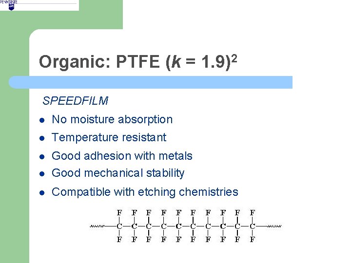
Organic: PTFE (k = 1. 9)2 SPEEDFILM l No moisture absorption l Temperature resistant l l Good adhesion with metals Good mechanical stability l Compatible with etching chemistries
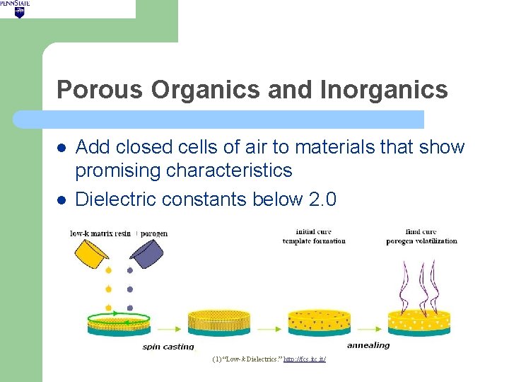
Porous Organics and Inorganics l l Add closed cells of air to materials that show promising characteristics Dielectric constants below 2. 0 (1) “Low-k Dielectrics. ” http: //fcs. itc. it/
Disadvantages of Porous Materials 2 l Weakens mechanical properties l Lower thermal conductivity l Narrow pore distribution to ensure dielectric constant is homogeneous and isotropic l Pores need to be closed cells to prevent crack propagation and moisture absorption l Need to add silica to seal surface pores
Air Gaps and Bridges (k = 1. 0)2 l Low breakdown voltage l Low thermal conductivity l Low strength l Deposition method unknown
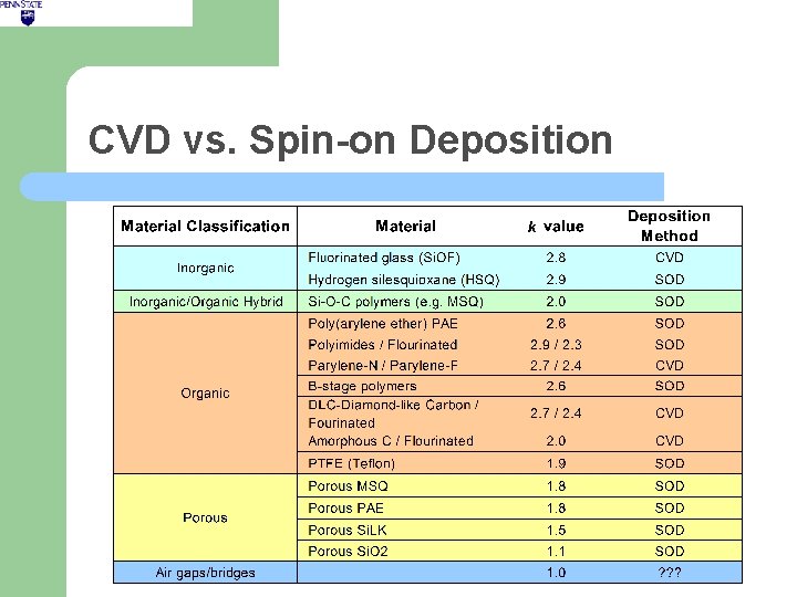
CVD vs. Spin-on Deposition
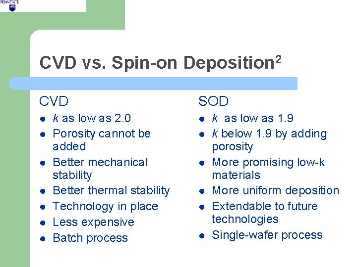
CVD vs. Spin-on Deposition 2 CVD l l l l k as low as 2. 0 Porosity cannot be added Better mechanical stability Better thermal stability Technology in place Less expensive Batch process SOD l l l k as low as 1. 9 k below 1. 9 by adding porosity More promising low-k materials More uniform deposition Extendable to future technologies Single-wafer process
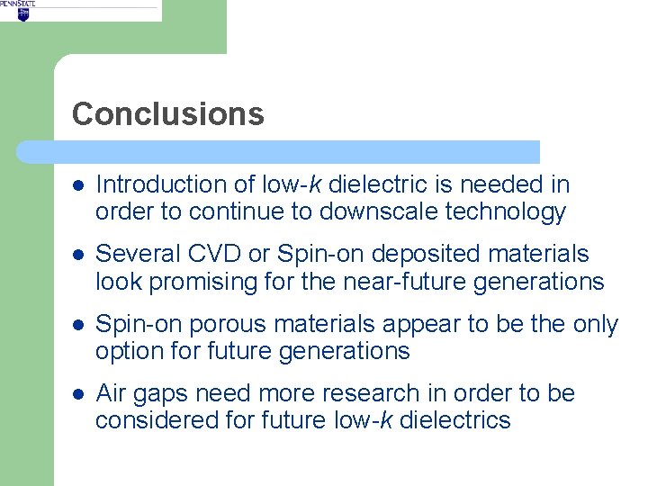
Conclusions l Introduction of low-k dielectric is needed in order to continue to downscale technology l Several CVD or Spin-on deposited materials look promising for the near-future generations l Spin-on porous materials appear to be the only option for future generations l Air gaps need more research in order to be considered for future low-k dielectrics
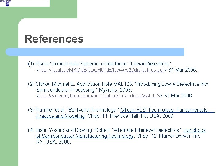
References (1) Fisica Chimica delle Superfici e Interfacce. “Low-k Dielectrics. ” <http: //fcs. itc. it/MAMe. BROCHURE/low-k%20 dielectrics. pdf> 31 Mar 2006. (2) Clarke, Michael E. Application Note MAL 123: “Introducing Low-k Dielectrics into Semiconductor Processing. ” Mykrolis. 2003. <http: //www. mykrolis. com/publications. nsf/ docs/MAL 123> 31 Mar 2006 (3) Plumber et al. “Back-end Technology. ” Silicon VLSI Technology: Fundamentals, Practice and Modeling. Chap. 11. Prentice Hall, NJ, USA. 2000. (4) Nishi, Yoshio and Doering, Robert. “Alternate Interlevel Dielectrics. ” Handbook of Semiconductor Manufacturing Technology. Chap. 12. Marcel Dekker, Inc. NY, USA. 2000.
- Slides: 18