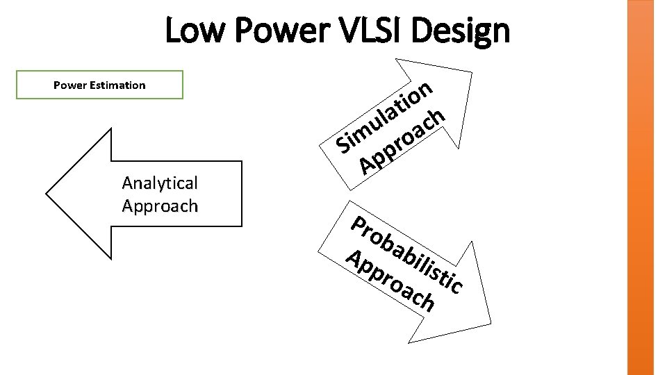
Low Power VLSI Design Power Estimation Analytical Approach



- Slides: 75

Low Power VLSI Design Power Estimation Analytical Approach n o i t a l h c u a m o i S pr Ap Pro ba Ap bil pro isti ach c

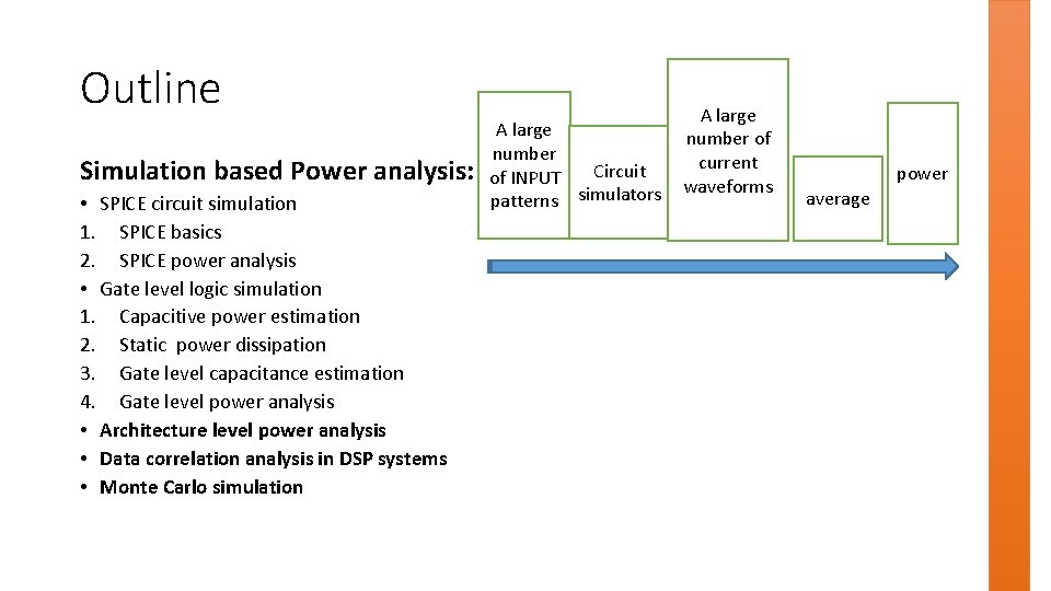
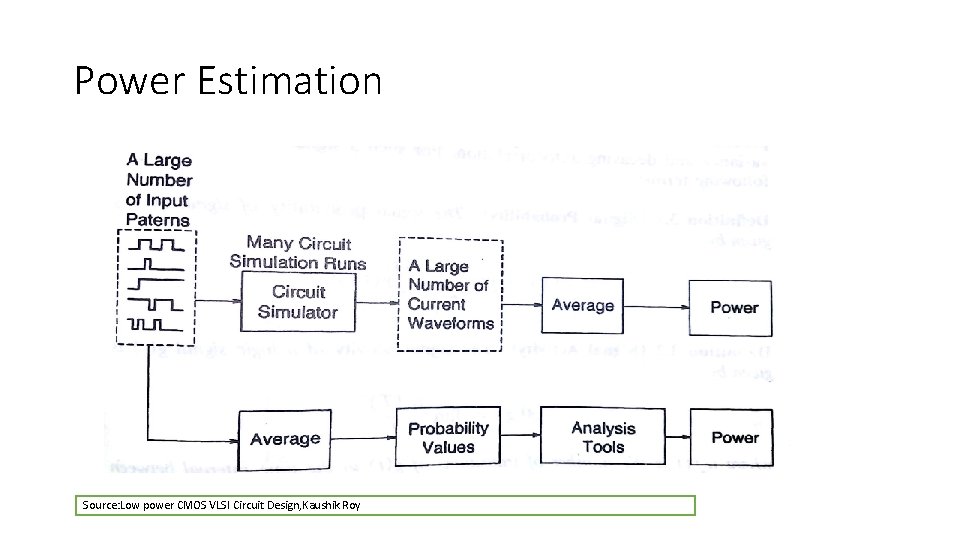
Outline Simulation based Power analysis: • SPICE circuit simulation 1. SPICE basics 2. SPICE power analysis • Gate level logic simulation 1. Capacitive power estimation 2. Static power dissipation 3. Gate level capacitance estimation 4. Gate level power analysis • Architecture level power analysis • Data correlation analysis in DSP systems • Monte Carlo simulation A large number Circuit of INPUT patterns simulators A large number of current waveforms power average

objectives Simulation techniques used to estimate and analyse power dissipation of VLSI chips

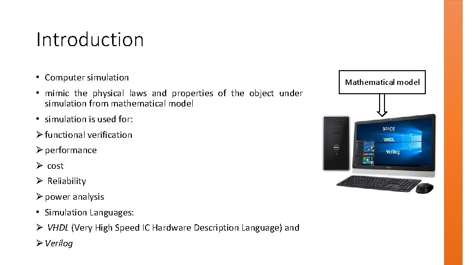
Introduction • Computer simulation • mimic the physical laws and properties of the object under simulation from mathematical model • simulation is used for: Ø functional verification Ø performance Ø cost Ø Reliability Ø power analysis • Simulation Languages: Ø VHDL (Very High Speed IC Hardware Description Language) and Ø Verilog Mathematical model

INTRODUCTION • VLSI design at various level of abstraction • Device level power Analysis • Circuit Level Power Analysis • Gate Level Power Analysis • RTL level • Architecture level • System level

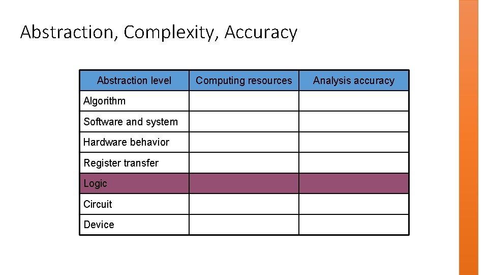
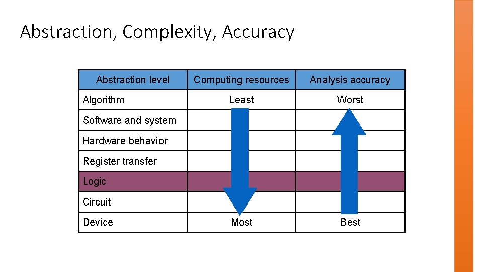
Abstraction, Complexity, Accuracy Abstraction level Algorithm Software and system Hardware behavior Register transfer Logic Circuit Device Computing resources Analysis accuracy

Abstraction, Complexity, Accuracy Abstraction level Algorithm Computing resources Analysis accuracy Least Worst Most Best Software and system Hardware behavior Register transfer Logic Circuit Device

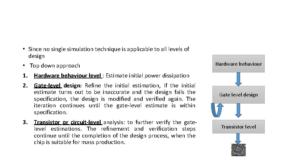
• Since no single simulation technique is applicable to all levels of design • Top down approach Hardware behaviour 1. Hardware behaviour level : Estimate initial power dissipation 2. Gate-level design: Refine the initial estimation, If the initial estimate turns out to be inaccurate and the design fails the specification, the design is modified and verified again. The iteration continues until the gate-level estimate is within specification. 3. Transistor or circuit-level analysis: to further verify the gatelevel estimations. The refinement and verification steps continue until the completion of the design process, when the chip is suitable for mass production. Gate level design Transistor level

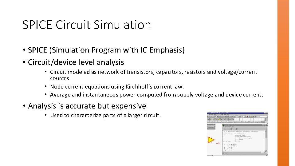
SPICE Circuit Simulation • SPICE (Simulation Program with IC Emphasis) • Circuit/device level analysis • Circuit modeled as network of transistors, capacitors, resistors and voltage/current sources. • Node current equations using Kirchhoff’s current law. • Average and instantaneous power computed from supply voltage and device current. • Analysis is accurate but expensive • Used to characterize parts of a larger circuit.

SPICE Power Analysis • Higher accuracy & More versatile tool • All types of power analysis • Component capacity • More resources for complex circuits • Memory or computation resources for complex circuits • Entire chip simulation is not possible • Extreme case analysis due to process variations • TYPICAL, BEST and WORST case conditions based on device speed

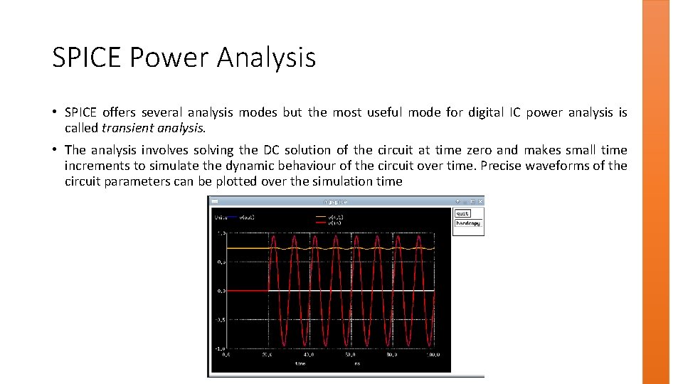
SPICE Power Analysis • SPICE offers several analysis modes but the most useful mode for digital IC power analysis is called transient analysis. • The analysis involves solving the DC solution of the circuit at time zero and makes small time increments to simulate the dynamic behaviour of the circuit over time. Precise waveforms of the circuit parameters can be plotted over the simulation time

• SPICE device models are derived from a characterization process. • Each device model is described by dozens of parameters. • The models are typically calibrated with physical measurements taken from actual test chips and can achieve a very high degree of accuracy.

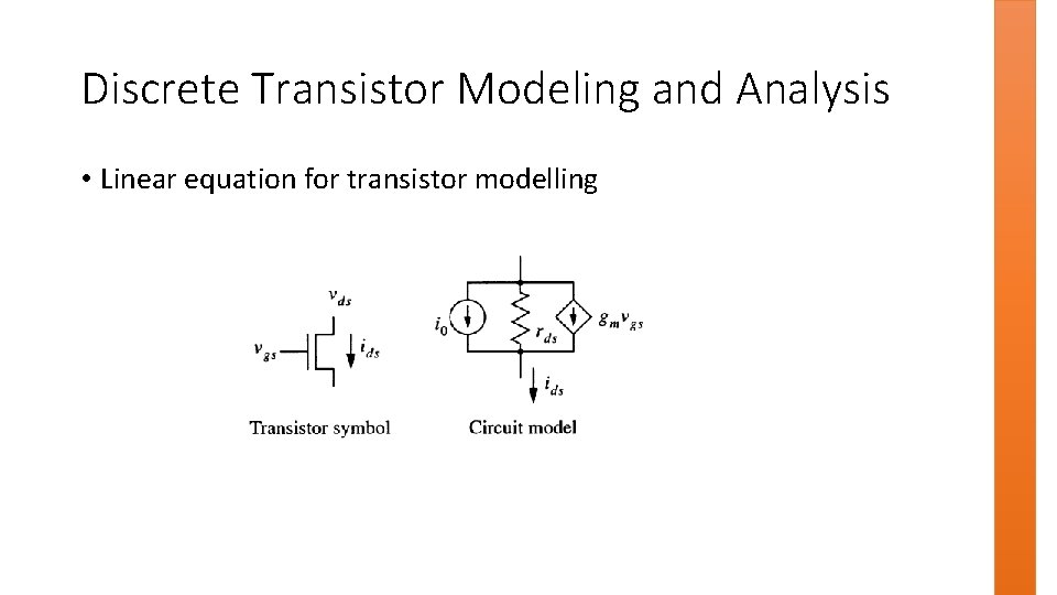
Discrete Transistor Modeling and Analysis • Linear equation for transistor modelling

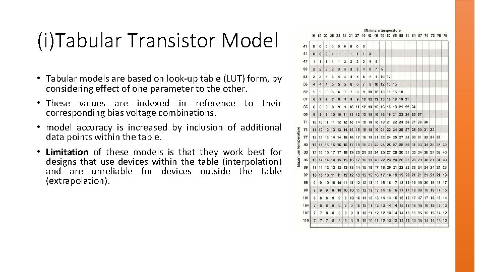
(i)Tabular Transistor Model • Tabular models are based on look-up table (LUT) form, by considering effect of one parameter to the other. • These values are indexed in reference to their corresponding bias voltage combinations. • model accuracy is increased by inclusion of additional data points within the table. • Limitation of these models is that they work best for designs that use devices within the table (interpolation) and are unreliable for devices outside the table (extrapolation).

• Even with the increased capacity, transistor-level tools are often not able to perform full-chip power analysis of very large scale chips. • The analysis speed is still several orders of magnitude slower than logic-level simulation. Chips with up to a hundred thousand transistors can be handled by transistor-level tools but many VLSI chips today exceed that scale.

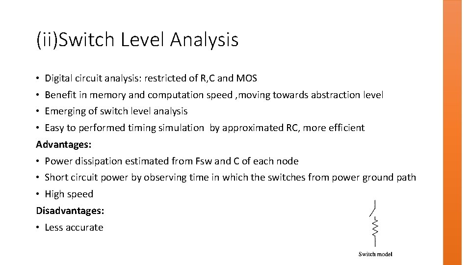
(ii)Switch Level Analysis • Digital circuit analysis: restricted of R, C and MOS • Benefit in memory and computation speed , moving towards abstraction level • Emerging of switch level analysis • Easy to performed timing simulation by approximated RC, more efficient Advantages: • Power dissipation estimated from Fsw and C of each node • Short circuit power by observing time in which the switches from power ground path • High speed Disadvantages: • Less accurate

Gate-level Logic Simulation • Simulation-based gate-level timing analysis: Mature method • Components: logic gates, Nets • full-chip simulation up to several million gates 1. Event-driven logic simulation • Events are zero-one logic switching of nets in a circuit • Event gate input to output with delay • Also support ‘unknown’, ’don’t care’ ‘high impedance’ state: more realistic • Verilog and VHDL are two popular languages

Example:

2. Cycle based simulation • Use of synchronous master clock • No arbitrary switching, based on schedule • Advantages: less number of switching events, increase efficient analysis

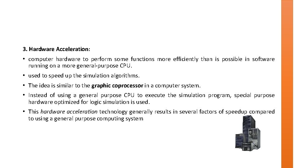
3. Hardware Acceleration: • computer hardware to perform some functions more efficiently than is possible in software running on a more general-purpose CPU. • used to speed up the simulation algorithms. • The idea is similar to the graphic coprocessor in a computer system. • Instead of using a general purpose CPU to execute the simulation program, special purpose hardware optimized for logic simulation is used. • This hardware acceleration technology generally results in several factors of speedup compared to using a general purpose computing system

4. hardware emulation. • Instead of simulating switching events using software programs, the logic network is partitioned into smaller manageable sub blocks. • The Boolean function of each sub-block is extracted and implemented with a hardware table mapping mechanism such as RAM or FPGA. • A reconfigurable interconnection network, carrying the logic signals, binds the sub-blocks together. • Circuits up to a million gates can be emulated with this technology but this is also the most expensive type of logic simulator to operate and maintain because of the sophisticated highspeed hardware required. • The simulation speed is only one to two orders of magnitude slower than the actual VLSI chips to be fabricated. For example, a 200 MHz CPU can be emulated with a 2 MHz clock rate, permitting moderate real time simulation.

1. Capacitive Power Dissipation • Gate-level power analysis based on logic simulation is one of the earliest power analysis tools developed. • The basic principle of such tools is to perform a logic simulation of the gate-level circuit to obtain the switching activity information. • The information is then used to derive the power dissipation of the circuit. • P= C V 2 f… • Frequency not possible with SPICE • Done by logic simulation, switching activity of each node monitored to get frequency • Fi= ti/2 T, T= simulation time

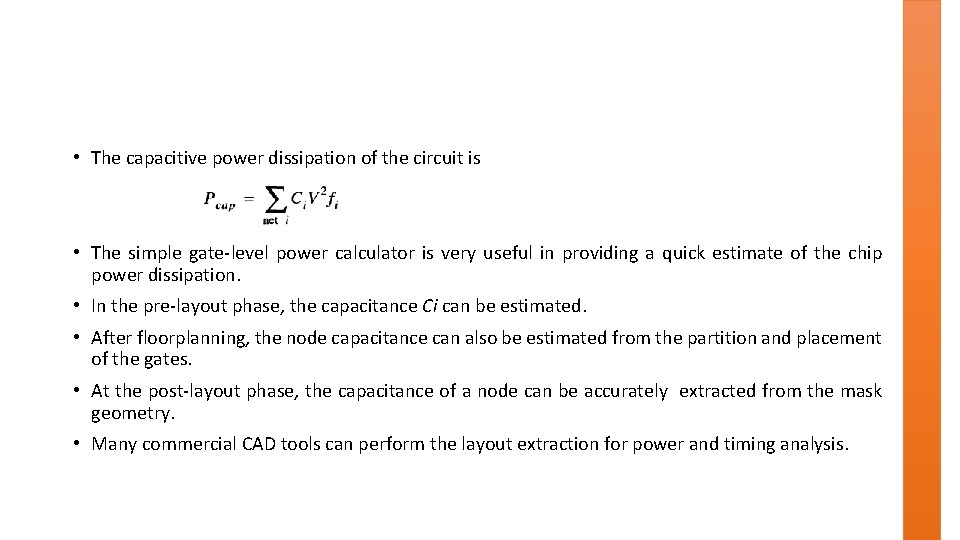
• The capacitive power dissipation of the circuit is • The simple gate-level power calculator is very useful in providing a quick estimate of the chip power dissipation. • In the pre-layout phase, the capacitance Ci can be estimated. • After floorplanning, the node capacitance can also be estimated from the partition and placement of the gates. • At the post-layout phase, the capacitance of a node can be accurately extracted from the mask geometry. • Many commercial CAD tools can perform the layout extraction for power and timing analysis.

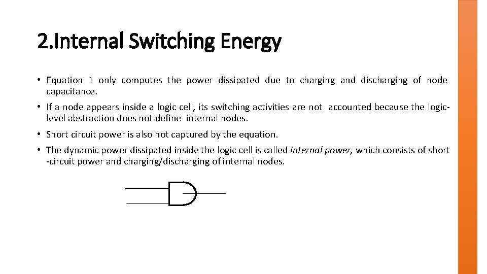
2. Internal Switching Energy • Equation 1 only computes the power dissipated due to charging and discharging of node capacitance. • If a node appears inside a logic cell, its switching activities are not accounted because the logiclevel abstraction does not define internal nodes. • Short circuit power is also not captured by the equation. • The dynamic power dissipated inside the logic cell is called internal power, which consists of short -circuit power and charging/discharging of internal nodes.

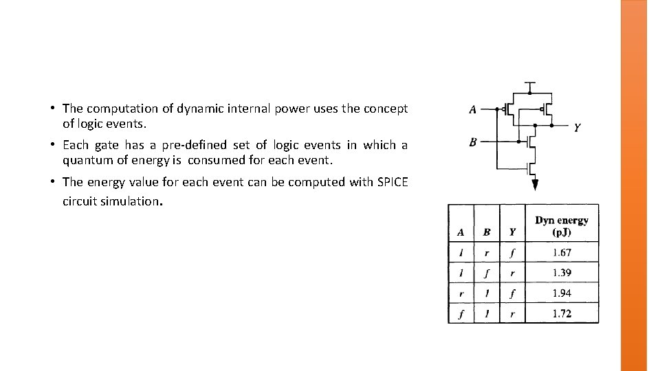
• For a simple logic gate, the internal power consumed by the gate can be computed through a characterization process similar to that of timing analysis for logic gates • The idea is to simulate the "dynamic energy dissipation events" of the gate with SPICE or other lower-level power simulation tools. • For example, in a NAND gate with inputs A, B and output Y, the logic event "A = 1, B switches from 0 to 1" causes the output to switch from 1 to 0 and consumes some amount of dynamic energy internally. • The energy is caused by short-circuit current or charging/discharging of internal nodes in the gate. • The dynamic energy dissipation event can be easily observed during logic simulation.

• The computation of dynamic internal power uses the concept of logic events. • Each gate has a pre-defined set of logic events in which a quantum of energy is consumed for each event. • The energy value for each event can be computed with SPICE circuit simulation.

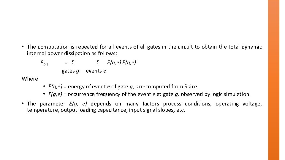
• The computation is repeated for all events of all gates in the circuit to obtain the total dynamic internal power dissipation as follows: Pint = Σ gates g Σ E(g, e) F(g, e) events e Where • E(g, e) = energy of event e of gate g, pre-computed from Spice. • F(g, e) = occurrence frequency of the event e at gate g, observed by logic simulation. • The parameter E(g, e) depends on many factors process conditions, operating voltage, temperature, output loading capacitance, input signal slopes, etc.

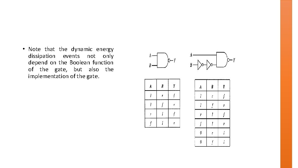
• Note that the dynamic energy dissipation events not only depend on the Boolean function of the gate, but also the implementation of the gate.

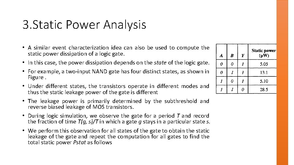
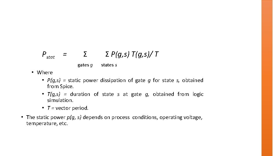
3. Static Power Analysis • A similar event characterization idea can also be used to compute the static power dissipation of a logic gate. • In this case, the power dissipation depends on the state of the logic gate. • For example, a two-input NAND gate has four distinct states, as shown in Figure. • Under different states, the transistors operate in different modes and thus the static leakage power of the gate is different • The leakage power is primarily determined by the subthreshold and reverse biased leakage of MOS transistors. • During logic simulation, we observe the gate for a period T and record the fraction of time T(g, s)/T in which a gate g stays in a particular state s. • We perform this observation for all states of the gate to obtain the static leakage of the gate and repeat the computation for all gates to find the total static power Pstat as follows

Pstat = Σ Σ P(g, s) T(g, s)/ T gates g states s • Where • P(g, s) = static power dissipation of gate g for state s, obtained from Spice. • T(g, s) = duration of state s at gate g, obtained from logic simulation. • T = vector period. • The static power p(g, s) depends on process conditions, operating voltage, temperature, etc.

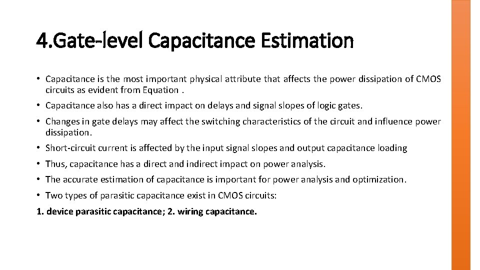
4. Gate-level Capacitance Estimation • Capacitance is the most important physical attribute that affects the power dissipation of CMOS circuits as evident from Equation. • Capacitance also has a direct impact on delays and signal slopes of logic gates. • Changes in gate delays may affect the switching characteristics of the circuit and influence power dissipation. • Short-circuit current is affected by the input signal slopes and output capacitance loading • Thus, capacitance has a direct and indirect impact on power analysis. • The accurate estimation of capacitance is important for power analysis and optimization. • Two types of parasitic capacitance exist in CMOS circuits: 1. device parasitic capacitance; 2. wiring capacitance.

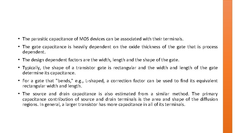
• The parasitic capacitance of MOS devices can be associated with their terminals. • The gate capacitance is heavily dependent on the oxide thickness of the gate that is process dependent. • The design dependent factors are the width, length and the shape of the gate. • Typically, the shape of a transistor gate is rectangular and the width and length of the gate determine its capacitance. • For a gate that "bends, " e. g. , L-shaped, a correction factor can be used to find its equivalent rectangular width and length. • The source and drain capacitance is also estimated from a similar method. The primary capacitance contribution of source and drain terminals is the area and shape of the diffusion regions. In general, a larger transistor has more capacitance in all of its terminals.

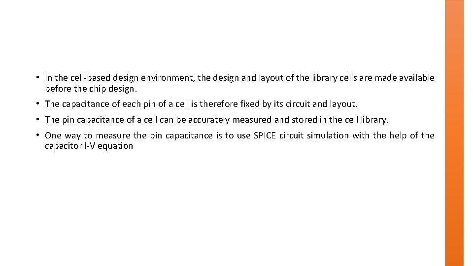
• In the cell-based design environment, the design and layout of the library cells are made available before the chip design. • The capacitance of each pin of a cell is therefore fixed by its circuit and layout. • The pin capacitance of a cell can be accurately measured and stored in the cell library. • One way to measure the pin capacitance is to use SPICE circuit simulation with the help of the capacitor I-V equation

• We vary the pin voltage ∆V of the cell in time ∆ T and observe the current i to obtain the capacitance C. • This measurement can be performed during the characterization of the cell.

• The second source of parasitic capacitance is wiring capacitance. • Wiring capacitance depends on the layer, area and shape of the wire. Typically, the width of routing wires is set to the minimum and the wiring capacitance is estimated from the lengths of the wires. • In practice, the process dependent factors of wiring capacitance are expressed by a capacitanceper-unit-length parameter that depends on the thickness of the wire, its distance from the substrate and its width. • Once the length of a wire is known, wiring capacitance can be computed.

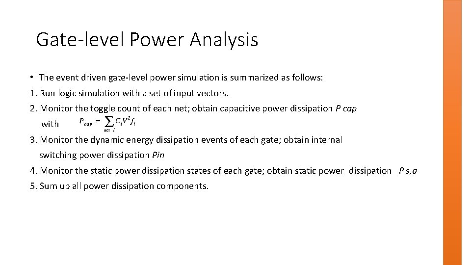
Gate-level Power Analysis • The event driven gate-level power simulation is summarized as follows: 1. Run logic simulation with a set of input vectors. 2. Monitor the toggle count of each net; obtain capacitive power dissipation P cap with 3. Monitor the dynamic energy dissipation events of each gate; obtain internal switching power dissipation Pin 4. Monitor the static power dissipation states of each gate; obtain static power dissipation P s, a 5. Sum up all power dissipation components.

Gate-Level Power Analysis • Sum up all three components of power: P = Pcap + Pint + Pstat 37

• The static and internal power dissipation of a gate depends on several factors such as the operating voltage and temperature, output load capacitance, input signal slopes, fabrication process, etc. • To capture the power dissipation variation due to such conditions, case analysis can be applied. • The gate is simulated with SPICE for all possible conditions that can affect the power. The results are stored in a multi-dimensional table after cells are characterized. • During analysis, the actual conditions of the circuit under simulation are specified by the user and the correct internal power or energy values will be used for analysis

• An automated power characterization and analysis tool using this technique has been reported. • The analysis speed of a gate-level tool is fast enough to allow full-chip simulation. • With the static and internal power characterization mentioned above, the accuracy within 10 -15% of SPICE simulation is possible. Commercial CAD tools based on this analysis method have been introduced.

• Detailed power dissipation of the logic network can be obtained with a simulation technique. • For example, we can observe the power dissipation on a per-gate or per-net basis. • We can compute the power dissipation of a module to determine the width of the power supply and ground lines to the module. • Coupled with layout information, we can plot the temperature profile of the chip to detect regions with potential reliability problems.

• A major disadvantage of gate-level analysis is that signal glitches cannot be modelled precisely. • Signal glitches are inherently analog phenomena and the simplified zero one logic model in gatelevel analysis fails to capture their effects. • The presence of glitches is very sensitive to the signal and gate delays of the circuit. Signal glitches can be a significant source of power dissipation in some VLSI circuits, as such cannot be ignored. • However, it is difficult for any analysis model above the logic level to account for the signal glitches precisely. • Some attempts to analyze glitches using probabilistic techniques have been reported. • One technique uses probability to express the presence of glitches but the unpredictable nature of signal glitches prohibits a precise deterministic analysis.

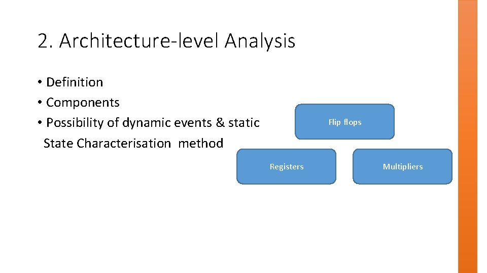
2. Architecture-level Analysis • Definition • Components • Possibility of dynamic events & static State Characterisation method Flip flops Registers Multipliers

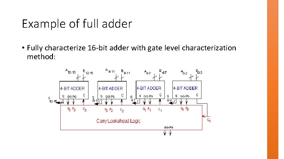
Example of full adder • Fully characterize 16 -bit adder with gate level characterization method:

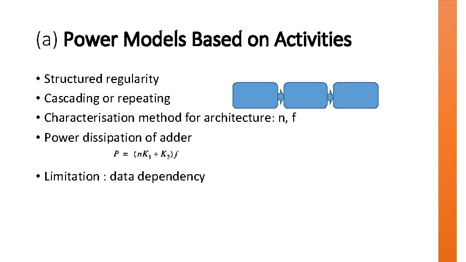
(a) Power Models Based on Activities • Structured regularity • Cascading or repeating • Characterisation method for architecture: n, f • Power dissipation of adder • Limitation : data dependency

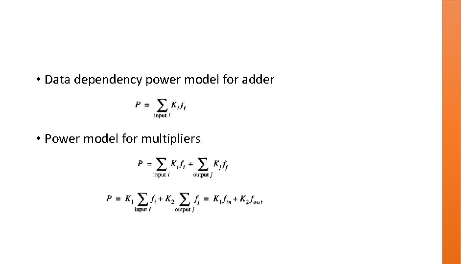
• Data dependency power model for adder • Power model for multipliers

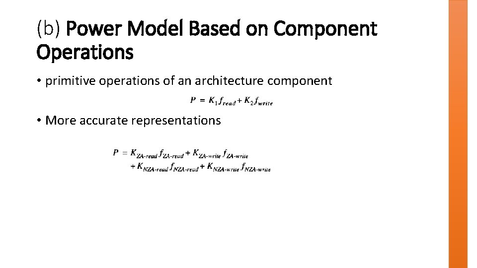
(b) Power Model Based on Component Operations • primitive operations of an architecture component • More accurate representations

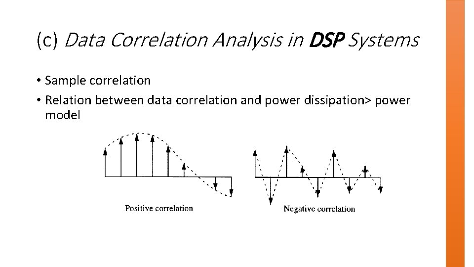
(c) Data Correlation Analysis in DSP Systems • Sample correlation • Relation between data correlation and power dissipation> power model

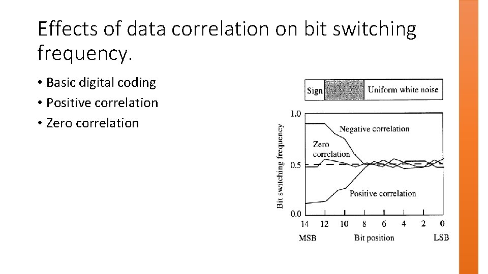
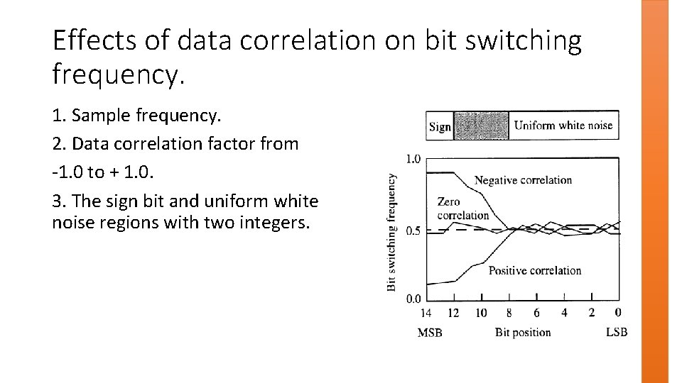
Effects of data correlation on bit switching frequency. • Basic digital coding • Positive correlation • Zero correlation

Effects of data correlation on bit switching frequency. 1. Sample frequency. 2. Data correlation factor from -1. 0 to + 1. 0. 3. The sign bit and uniform white noise regions with two integers.

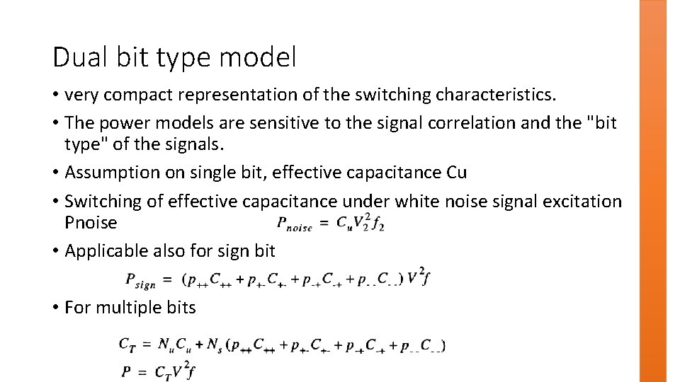
Dual bit type model • very compact representation of the switching characteristics. • The power models are sensitive to the signal correlation and the "bit type" of the signals. • Assumption on single bit, effective capacitance Cu • Switching of effective capacitance under white noise signal excitation Pnoise • Applicable also for sign bit • For multiple bits

Challenges in Architecture level • Large number of I/O pins restrict the use of logic events • Which parameters have major influence on power dissipation? Size, signal frequency, operation frequency… • What is a relationship of the power dissipation with the chosen parameters ? Equation or lookup table

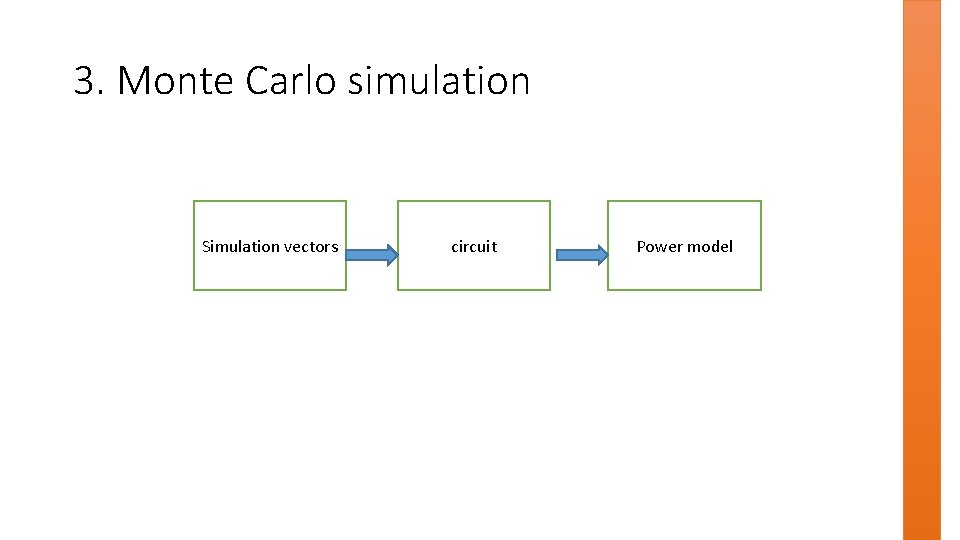
3. Monte Carlo simulation Simulation vectors circuit Power model

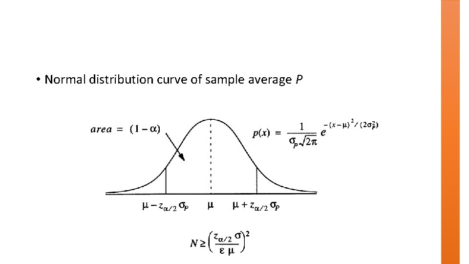
• But is it necessary wasting computer resources to simulate that many vectors? • How much extra accuracy can we achieve by simulating a million vectors versus only a thousand vectors? How do we know that we have simulated enough vector length? • All these lead to an important question of the stopping criteria of the simulation: • when do we stop simulation so that the result is accurate enough for our purpose?

• Normal distribution curve of sample average P

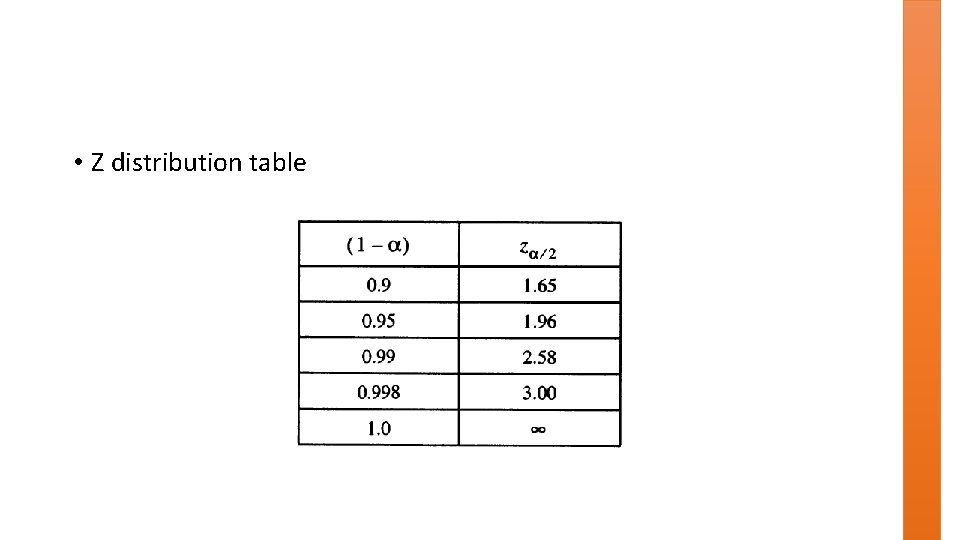
• Z distribution table

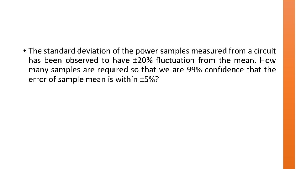
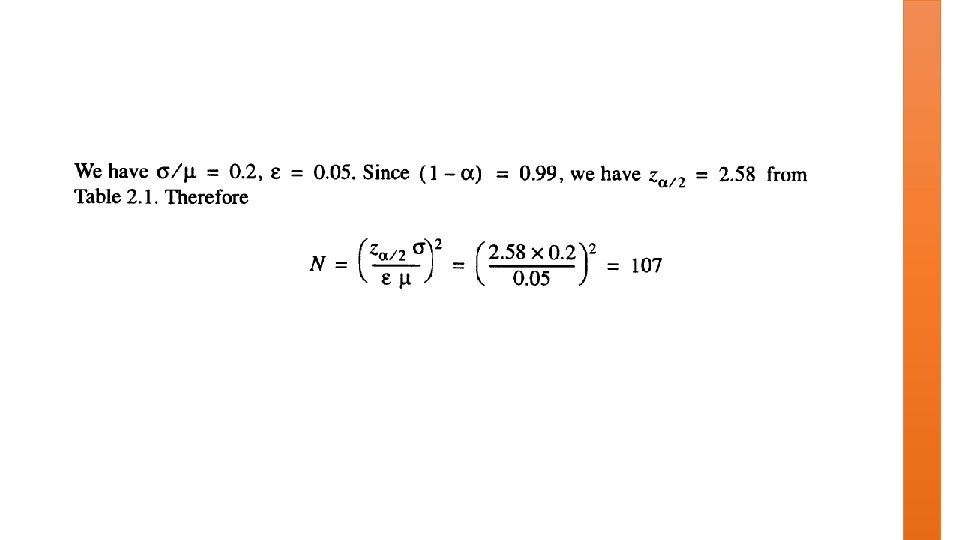
• The standard deviation of the power samples measured from a circuit has been observed to have ± 20% fluctuation from the mean. How many samples are required so that we are 99% confidence that the error of sample mean is within ± 5%?


Probabilistic Power Analysis

simulation approach to power analysis • mimic the circuit behaviour over time, based on a predictable power model. • Often the power model is built from a lower-level abstraction process called characterization. • The simulation approach is very computation intensive. In some cases, we need to solve the voltage or current of the circuit, while in others, we need to simulate the exact time instant on which a certain event occurs in the circuit. • In logic simulation, all signal events are recorded precisely by the simulation software. The events are then tabulated and averaged over time to obtain the actual average power dissipation of the circuit.

objectives • very different from simulation-based approaches. • A logic signal is viewed as a random zero-one process with certain statistical characteristics. • We no longer know the exact event time of each logic signal switching. • Instead, we only prescribe or derive several numerical statistical characteristics of the signal. • The power dissipation of the circuit is then derived from the statistical quantities.

Power Estimation Source: Low power CMOS VLSI Circuit Design, Kaushik Roy

• computation efficiency: number of statistical quantities to be analysed is generally orders of magnitude smaller than the number of events to be processed compared to the simulation approach. • The application of probabilistic power analysis techniques has mainly developed for gate-level abstraction and above.

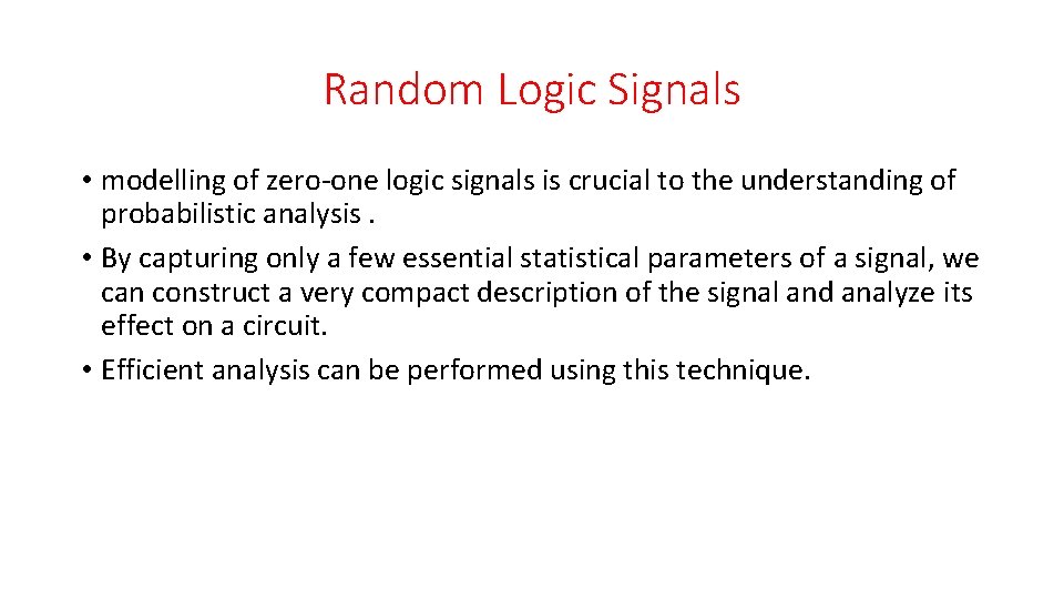
Random Logic Signals • modelling of zero-one logic signals is crucial to the understanding of probabilistic analysis. • By capturing only a few essential statistical parameters of a signal, we can construct a very compact description of the signal and analyze its effect on a circuit. • Efficient analysis can be performed using this technique.

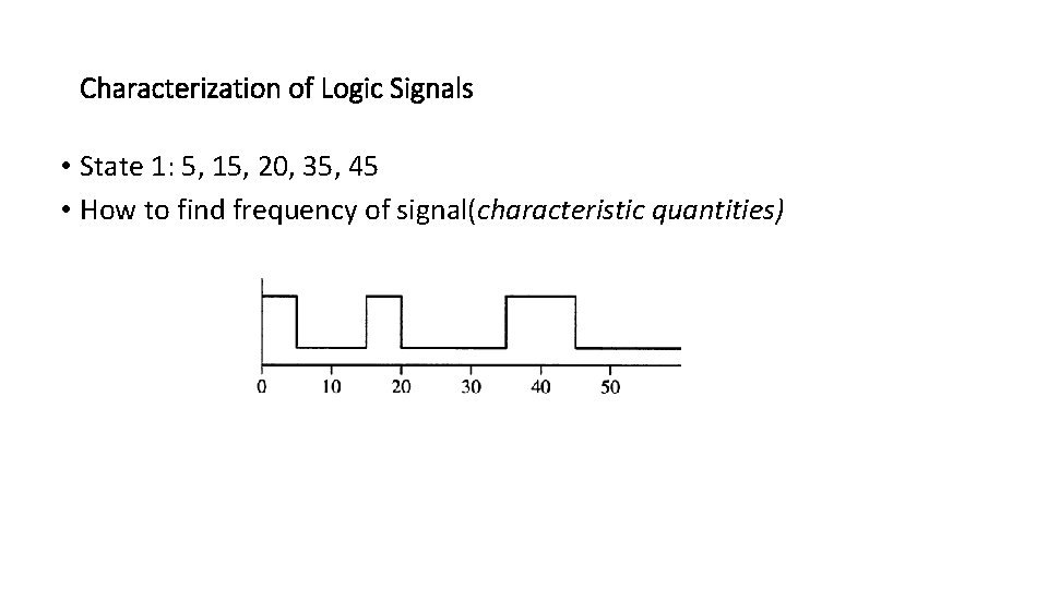
Characterization of Logic Signals • State 1: 5, 15, 20, 35, 45 • How to find frequency of signal(characteristic quantities)

Characterization of Logic Signals

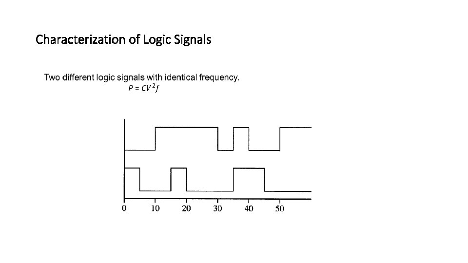
• By describing only the frequency of the signal, we can reduce the computation requirements. • Formation of signal class • But , signal characterization is that signals are no longer uniquely identified. • We only know that a logic signal makes some number of transitions per unit time but the exact instant at which each individual transition occurs is not known.

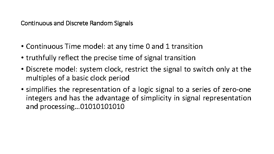
Continuous and Discrete Random Signals • Continuous Time model: at any time 0 and 1 transition • truthfully reflect the precise time of signal transition • Discrete model: system clock, restrict the signal to switch only at the multiples of a basic clock period • simplifies the representation of a logic signal to a series of zero-one integers and has the advantage of simplicity in signal representation and processing… 0101010

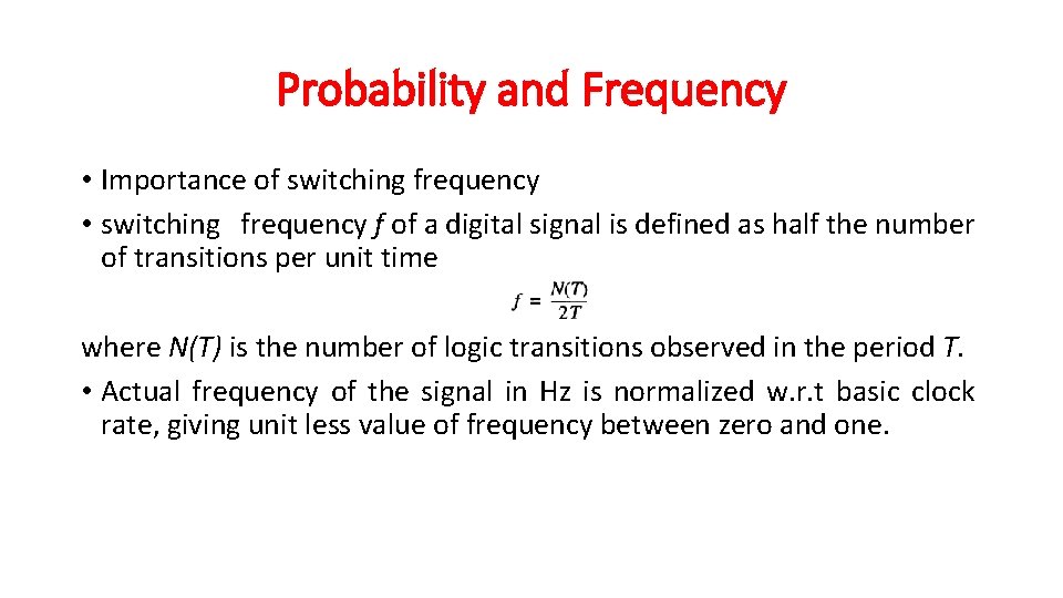
Probability and Frequency • Importance of switching frequency • switching frequency f of a digital signal is defined as half the number of transitions per unit time where N(T) is the number of logic transitions observed in the period T. • Actual frequency of the signal in Hz is normalized w. r. t basic clock rate, giving unit less value of frequency between zero and one.

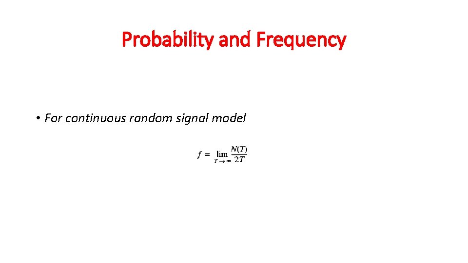
Probability and Frequency • For continuous random signal model

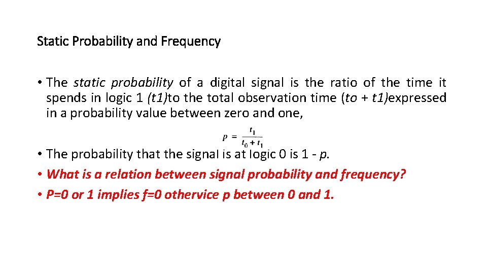
Static Probability and Frequency • The static probability of a digital signal is the ratio of the time it spends in logic 1 (t 1)to the total observation time (to + t 1)expressed in a probability value between zero and one, • The probability that the signal is at logic 0 is 1 - p. • What is a relation between signal probability and frequency? • P=0 or 1 implies f=0 othervice p between 0 and 1.

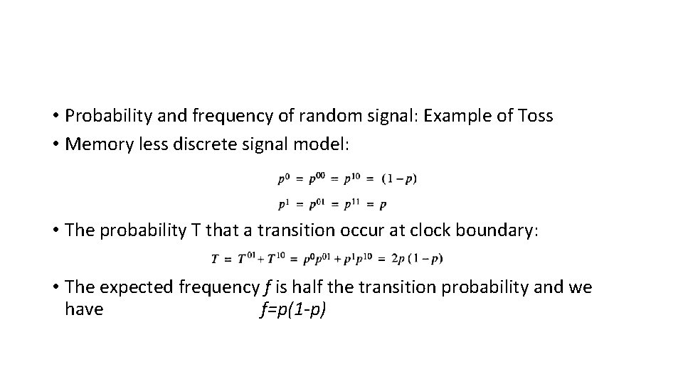
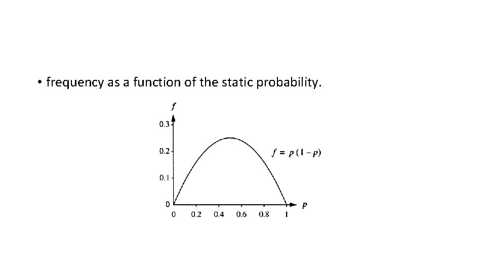
• Probability and frequency of random signal: Example of Toss • Memory less discrete signal model: • The probability T that a transition occur at clock boundary: • The expected frequency f is half the transition probability and we have f=p(1 -p)

• frequency as a function of the static probability.

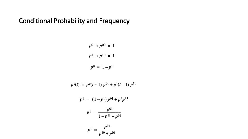
Conditional Probability and Frequency

Probabilistic power analysis techniques
